Large LFMR observed in twinned thin films epitaxially grown on YSZ-buffered SOI substrate
Abstract
thin films have been grown on yttria-stabilized zirconia (YSZ) buffered silicon-on-insulator (SOI) substrate by the pulsed laser deposition technique. While full cube-on-cube epitaxy was achieved for the YSZ layer, the top manganite layer was multi-domain-oriented, with a coexistence of cube-on-cube and cube-on-diagonal epitaxy. Due to a combined influence from the magnetocrystalline anisotropy and the magnetoelastic anisotropy, in zero field the local spin orientation varies across the twin boundaries. As a result, a quite large low-field magnetoresistance (LFMR) based on spin-dependent tunnelling was observed. The film shows a resistance change of 20% in a magnetic field 1000 Oe at 50 K, which is promising for real applications.
pacs:
75.47.Lx; 75.70.Ak; 72.25.MkManganite materials with perovskite structure have attracted considerable attention during the past decade, since a ‘colossal magnetoresistance’ occurs around their Curie temperature Jin1 ; Jin2 . Potential applications such as new-generation magnetic sensors or reading heads are ardently anticipated. Numerous efforts have been made to prepare manganite thin films on single-crystalline substrates of SrTiO3, LaAlO3, MgO, and the yttria-stabilized zirconia (YSZ). However, in order to realize an integration with the existing silicon manufacturing technology, it is practically important to grow high quality manganite thin films on silicon wafers. Nevertheless a silicon substrate is unfavorable for a full epitaxy growth, due to not only its large lattice and thermal expansion mismatch with the manganites, but also its easily oxidized surface and severe chemical inter diffusion. Therefore up to now high quality manganite thin films were achieved only through heteroepitaxial growth with several transition layers Wong ; Fontcuberta ; Kim . Lately, in the semiconductor industry a new technology, SOI (silicon on insulator), has become prevailing Shahidi . It has been suggested to take advantage of the buried polycrystalline silicon dioxide (SiO2) in the wafer as a compliant layer to relax the strain between the films and the substrate, then high quality crack-free thin films can be obtained on single-layer-buffered SOI substrate Kang ; Wang . In this letter, we report the growth of (LCMO) thin films on YSZ-buffered SOI substrate. A unique crystallographic domain structure with a high density of 45∘ twins were observed. As a result the LFMR is enhanced due to the spin-dependent tunnelling across the twin boundaries.
We adopted commercial p-type SIMOX (100)SOI wafers provided by Shanghai Simgui. Prior to the film deposition, the SOI substrate was ultrasonically cleaned in diluted phosphoric acid (4%), deionized water, alcohol and acetone sequentially to remove contaminations from its surface, but leave the topmost native SiO2 layer untouched. The films were grown by the pulsed laser deposition technique using a KrF excimer laser. The YSZ target was a single crystal, while the LCMO target was a stoichiometric ceramic. The chamber was evacuated down to Pa before the heating started in order to avoid further surface oxidation. The YSZ buffer layer was grown in the background vacuum at a substrate temperature () of 820∘C and a laser repeat rate of 7 Hz. The LCMO thin film was then deposited in situ in an oxygen pressure of 40 Pa on YSZ at of 860∘C and a repeat rate of 2 Hz. High purity oxygen was injected in immediately after the film deposition, then the films were cooled down in 1 atm oxygen at a ramp rate of 40∘C/min to room temperature. The film thickness was around 100 nm for YSZ and 150 nm for LCMO.
Growth of the YSZ layer was monitored in situ by a real-time RHEED, while the in-plane crystallinity and the morphology of the LCMO layer was checked by RHEED at room temperature after the film deposition. The film out-of-plane orientation and crystallinity were characterized by x-ray diffraction (XRD) - scan and -scan. The electrical resistivity () and the magnetoresistance (MR) of the films were measured by using a standard four-probe technique. An MPMS 5 superconducting quantum interference device (SQUID) was employed to generate uniform magnetic field for both MR and magnetization measurements.
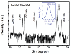
Figure 1 shows a typical XRD - spectrum of the LCMO/YSZ/SOI heterostructure. In the figure, the LCMO thin film is indexed as a pseudocubic structure. Besides the reflections from Si substrate, only the (200) and (400) of YSZ and the (001) and (002) of LCMO are observed, revealing the full c-axis texture of the film. Here Si(200) appears due to the long time heating during the film deposition. The out-of-plane lattice parameters derived are 5.15 Å for YSZ and 3.82 Å for LCMO. The inset is the rocking curve of the LCMO(002). Its full width at half maximum (FWHM) is about 0.95∘, indicating a small mosaic spread along c-axis in the film.
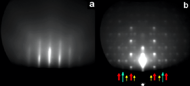
The in-plane orientations of the bilayer were determined by RHEED observations. The incident electron beam was along Si[100]. After the first five to ten laser pulses, we noted that the RHEED pattern of SOI substrate faded out, implying that the first several YSZ atomic layers are of poor crystallinity. This most probably originates from the native amorphous SiO2 layer on the SOI surface. Nevertheless, 30 seconds later, a blur and thick streaklike diffraction pattern of YSZ[100] appeared. With increase of the deposition time and thus increase of the film thickness, the intensity and sharpness of the diffraction pattern gradually increased, suggesting a recover of the YSZ crystallinity. Fig. 2(a) was recorded after the YSZ film deposition. The very clear and sharp streaks strongly suggest perfect in-plane epitaxy of the film, as well as its 2D-like atomic smooth surface Wang2 . The LCMO thin film grown on YSZ, however, shows clear 3D characteristics, as seen in Fig. 2(b). The roundish instead of streaklike diffraction spots reveal that the surface of the LCMO film is rather rough. Furthermore, the film is clearly multi-oriented in plane. As indicated in the figure by thick arrows, the majority orientation is the LCMO(110) which is grown on YSZ in a cube-on-diagonal way. The minority is the cube-on-cube grown LCMO(100), as labelled by thinner short arrows. The very weak spots indicated by long thin arrows are due to the LCMO(120). Obviously there exists a high density of 45∘ and 63.4∘ twin boundaries in plane. Along LCMO(110), the lattice mismatch is -4.8%, so the film is compressively strained. On the contrary, along LCMO(100) the lattice mismatch is +7.3%, if we assume that every five LCMO unit cells occupy four YSZ unite cells, thus the film is tensilely strained. Therefore it is reasonable to conclude that a large strain exists in the film plane, which may help to explain the very rough film surface.
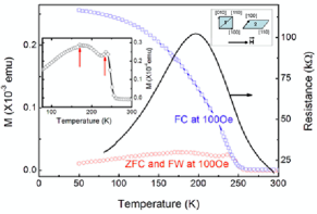
The curve of LCMO film is shown in Fig. 3. The film undergoes an insulator to metal transition at 195 K, significantly lower than that of the films grown on LaAlO3, which is around 260 K Vlakhov . The magnetization versus temperature curves, measured in a 100 Oe field applied in the film plane roughly along Si[100], are also plotted. The field-cooled (FC) line shows a broad paramagnetic to ferromagnetic transition with 250 K, comparable to that of the films grown on LaAlO3. The drop of behind in our film is due to the high-density crystallography defects (twin boundaries) in the film Blamire . It is worthy to note that the zero-field-cooled (ZFC) curve diverges a lot from the FC one. The magnetization moment (M) at 50 K under ZFC is more than 10 times lower than that under FC. Moreover, as seen in the inset, two peaks appear on the ZFC curve, corresponding to two blocking temperatures (TB): a sharp one at T K and a broad one near T K. We know that, at 0 K in zero field, the spins in the two crystallographic structures locate in their respective [100] easy axes ODonnell , as illustrated at the upper-right corner of Fig. 3. In addition, the magnetostriction constant along LCMO[100] is positive ODonnell , so the overall in-plane tensile strain in the direction perpendicular to the field is larger than that in the field direction, and thus the spins tend to align perpendicular to the field. Therefore due to the magnetocrystalline anisotropy of four-fold symmetry and the magnetoelastic anisotropy, the ZFC M measured at low temperatures is quite small. With increase of the temperature, the frozen spins will progressively rotate to the field direction, resulting in an increase of M. When the temperature is higher than , thermal fluctuations destroy the magnetic ordering gradually, and M declines again. It is clear that the spins move out from LCMO[100] is more difficult for structure 1 than for structure 2 due to the magnetoelastic anisotropy, therefore TB is higher for the former. Moreover, in the applied field, for 2 the spins will gradually rotate into the field direction, which is along its hard axes [110]. For 1, however, the spins will abruptly jump to the field direction after they cross over [110]. Therefore TB1 is sharper than TB2. The measured ZFC curve reveals an overall behavior of the two structures in the film.
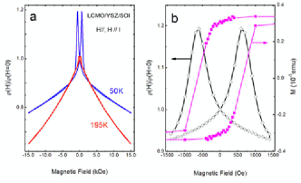
From the investigations on microstructure and magnetization of the LCMO film, a large extrinsic LFMR based on spin-dependent tunnelling across twin boundaries can be expected. The magnetoresistance measured in a field scanning from -1.5 to +1.5 tesla at and 50 K, respectively, are shown in Fig. 4(a). The field was applied roughly parallel to the measuring current, i.e. along Si[100] in the film plane. The film was cooled to the specified temperatures in zero field. While measured at 195 K shows a linear field dependence with a small coercivity and negligible shoulders, that measured at 50 K exhibits a smaller slope at high fields, but shows very sharp extrinsic peaks at low fields. Zoom-in of the peaks is shown in Fig. 4(b). For convenience, the magnetic hysteresis loop measured at the same temperature is also plotted. It is clear that the sample resistance peaks around 700 Oe, approximately the coercivity field, which corresponds to a state that the magnetic spins in individual structures incline to their respective easy axes, and thus the angle between spins in neighboring twins is the largest. A higher magnetic field can align the spins to the field direction and reduce the resistance drastically. The peak magnitude is really impressive, which is as high as 20% (defined as [R(Max.)-R(0)]/R(0)). That is, in a magnetic field range 0700 Oe, the resistivity changes for 20%. Up to now the only competitors were that obtained from ultrathin films Wang3 , or films with artificial grain boundaries Mathur . This provides an extraordinary large field sensitivity that can be utilized for real applications. As a matter of fact, the co-existence of two in-plane orientations may be a common feature of the manganite thin films grown on YSZ. We have noted that, Vlakhov et al. Vlakhov also observed a fairly large LFMR in the LCMO thin film grown on YSZ single-crystal substrate, as can be seen clearly in Fig. 2(b) of ref.Vlakhov , although the underlying mechanism was not mentioned in their paper.
In summary, we have successfully deposited thin films on YSZ-buffered SOI substrates. The top LCMO layer was multi-domain oriented with a high density of 45∘ twin boundaries. As a result, a quite large LFMR based on spin-dependent tunnelling was observed, which provides a most feasible solution for real applications.
References
- (1) S. Jin, T.H. Tiefel, M. McCormack, R.A. Fastnacht, R. Ramesh, and L.H. Chen, Science 264, 413(1994)
- (2) S. Jin, H.M. O’Bryan, T.H. Tiefel, M. McCormack, and W.W. Rhodes,Appl. Phys. Lett. 66, 382(1995)
- (3) K.H.Wong, and Y.S.Leung,Thin Solid Films 354, 55(1999)
- (4) J. Fontcuberta, M. Bibes, B. Martínez, V. Trtik, C. Ferrater, F. Sánchez, and M. Varela, J. Appl. Phys. 85, 4800(1999)
- (5) J.-H. Kim, S.I. Khartsev, and A.M. Grishin, Appl. Phys. Lett. 82, 4295(2003)
- (6) G. G. Shahidi, IBM J. Res. Dev. 46, 121(2002)
- (7) L. Kang, Z.F. Di, S.Z. Yang, Y.J. Feng and P.H. Wu, Supercond. Sci. Technol. 15, 320(2002)
- (8) P. Wang, J. Li, W. Peng, K. Chen, P. L. Lang, J. Y. Xiang, Y.F. Chen, X.P. Xu, H.Y. Tian and D.N. Zheng, Supercond. Sci. Technol. 17, 804(2004)
- (9) S.J. Wang and C.K. Ong, Appl. Phys. Lett. 80, 2541(2002)
- (10) E.S. Vlakhov, R.A. Chakalov, R.I. Chakalova, K.A. Nenkov, K.Dörr, A. Hanstein, and K.-H. Müller, J. Appl. Phys. 83, 2152(1998)
- (11) M.G. Blamire, B.-S. Teo, J.H. Durrell, N.D. Mathur, Z.H. Barber, J.L. McManus Driscoll, L.F. Cohen, J.E. Evetts, J. Mag. Mag. Mater. 191 359(1999)
- (12) J. O’Donnell, M.S. Rzchowski, J.N. Eckstein, and I. Bozovic, Appl. Phys. Lett. 72, 1775(1998)
- (13) H.S. Wang, Qi Li, Kai Liu, and C. L. Chien, Appl. Phys. Lett. 74, 2212(1999)
- (14) N.D. Mathur, G. Burnell, S.P. Issac, T.J. Jackson, B.-S. Teo, J.L. McManus Driscoll, L.F. Cohen, J.E. Evetts, M.G. Blamire, Nature 387 266(1997)