On leave from ]University of Havana, Cuba Present address: ]University of Chile, Faculty of Science, Las Palmeras 3425, Ñuñoa, Santiago, Chile. Also at ]Condensed Matter Theory Group, Uppsala University, Sweden. Present address: ]Centro de Investigaciones del Petróleo, Havana, Cuba.
Electronic structure of crystalline binary and ternary Cd-Te-O compounds
Abstract
The electronic structure of crystalline CdTe, CdO, -TeO2, CdTeO3 and Cd3TeO6 is studied by means of first principles calculations. The band structure, total and partial density of states, and charge densities are presented. For -TeO2 and CdTeO3, Density Functional Theory within the Local Density Approximation (LDA) correctly describes the insulating character of these compounds. In the first four compounds, LDA underestimates the optical bandgap by roughly 1 eV. Based on this trend, we predict an optical bandgap of 1.7 eV for Cd3TeO6. This material shows an isolated conduction band with a low effective mass, thus explaining its semiconducting character observed recently. In all these oxides, the top valence bands are formed mainly from the O 2p electrons. On the other hand, the binding energy of the Cd 4d band, relative to the valence band maximum, in the ternary compounds is smaller than in CdTe and CdO.
pacs:
71.20.Nr, 71.20.Ps,73.,81.05., 81.05.ZxI Introduction
Cadmium Telluride, CdTe, has been considered a prototype of II-VI semiconducting compounds for more than 30 years. It has found important applications in -ray detectors, infrared windows, solar cells and other optoelectronic devices.Zanio (1978) Having being the object of many of the early studies in semiconductor science, the difficulties found in obtaining high quality crystals hampered its research and applications in cutting edge electronic technology. Recently CdTe has received renewed interest due to the search for cheap technologies for mass production of solar cells that do not require high quality monocrystals. The fact that the fundamental absorption gap of CdTe lies in the region of maximum intensity of solar radiation makes it an important material for solar energy conversion on the earth. The solar cells based on heterojunctions of CdTe/CdS are a valuable option.
The development of a complete technology requires complementary materials that could be used for substrates, coats, contacts, gates, etc. Among these materials are the amorphous CdTe oxides obtained by r.f. sputtering, which have been extensively studied by optical spectroscopy, X-ray photoemission spectroscopy and Auger electron spectroscopy. Espinoza-Beltrán et al. (1991, 1993); Zapata-Navarro et al. (1994, 1997); El Azhari et al. (1997); Bartolo-Pérez et al. (1999); Caballero-Briones et al. (1998); Iribarren et al. (1999); Arizpe-Chávez et al. (2000); Iribarren et al. (2001); Bartolo-Pérez et al. (2002a, b) These alloys are transparent insulators whose optical gap can be tuned according to the content of oxygen between 1.5 and 4 eV, and can play a role in CdTe technology similar to that of SiO2 in Si technology. Native oxides have also been identified on CdTe surfaces. Ebina et al. (1980); Davis et al. (1981); Wang et al. (1987); Choi and Lucovsky (1988); Heiba (2003) However, given the difficulties produced by its amorphous structure, the structural and electronic properties of these materials are mostly unknown. Even the nature of oxides in CdTe surfaces is still a subject of controversy. Miotto et al. (2003)
The development of a thorough understanding of the electronic properties of the amorphous CdTe oxides require a careful study of the crystalline compounds of Cd, Te, and O. These compounds provide information about short range order and local electronic properties that are determinant in the amorphous regime. The Cd-Te-O compounds can also provide valuable information to help understand the processes of oxygen interaction with crystalline CdTe, including adsorption and diffusion.
Modern ab-initio simulation provides a powerful tool to study complex compounds and to predict structural properties with reasonable confidence. Although there are many reports of ab-initio calculations of Cd and Te compounds, including c-CdTe,Wei and Zunger (1988); Vogel et al. (1995, 1996); Albrecht et al. (1997) l-CdTe,Godlevsky et al. (1999) c-CdOBoettger and Kunz (1983); Jaffe et al. (1991); Vogel et al. (1996); Dou et al. (1998); Wang et al. (2001); Guerrero-Moreno and Takeuchi (2002)and TeOn clustersKowada et al. (1996); Ushino and Yoko (1996); Suehara et al. (1994, 1995); Berthereau et al. (1996); Suehara et al. (1998); Yakovlev et al. (2002), the crystalline TeO2 and the ternary compounds remain largely unexplored. Only one ab-initio study of a Cd-Te-O system, which addresses the O adsorption on CdTe surfaces, is known to the authors.Miotto et al. (2003) Despite being a profitable material for electromechanical and acoustooptical devices,Yakovlev et al. (2002) in the phase (paratellurite) even crystalline TeO2 has never been the object of a full electronic structure calculation.
The main difficulty for semi-empirical or ab initio simulation of Cd-Te-O compounds has been the large number of atoms per unit cell in the known phases, Thomas (1988); Madelung (1986a); Burckhardt et al. (1982); Kräemer and Brandt (1985) (e.g. 12 atoms in -TeO2, 24 in -TeO2, 20 in Cd3TeO6, 40 in CdTeO3, 224 in CdTe2O5). Moreover Cd atoms have ten electrons in level 4d which lie in the range of the valence band of Cd compounds and increase significantly the computer resources necessary for the calculations. In certain cases, the effect of the Cd 4d electrons can be represented with the help of pseudopotentials plus a partial core correction scheme; this approach has been successful for molecular dynamic simulations.Godlevsky et al. (1999) However, every use of this scheme needs to be tested, as the Cd 4d electrons are known to influence several important properties, e.g. the structure of the valence band, bandgaps, cohesive energy, and lattice parameter.Wei and Zunger (1988)
In this paper we report the first ever calculation of the electronic properties of crystalline -TeO2 (paratellurite), monoclinic CdTeO3 (Cadmium oxotellurate(IV)), and Cd3TeO6 (Cadmium hexaoxotellurate). In order to analyze the nature of the chemical bond in these materials, and to evaluate the systematic errors inherent to the theory, we also analyze the electronic structure of the simpler semiconducting compounds CdTe and CdO.
II Structural properties
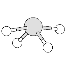
TeO2 is a mixed covalent-ionic insulator, the most abundant phase of which is -TeO2 or paratellurite. Paratellurite structure has a tetragonal lattice with four formula units per unit cell. The space group has been identified as P and P.Berndt (1997) In this work we have studied the electronic properties for the most recently reported.Thomas (1988) At the short-range level, the structural units of paratellurite are TeO4 trigonal bipyramids (tbp) with Te atoms at apex (see Fig. 1). The corners of the tbps are occupied by two equatorial oxygen atoms (Oeq), with Te-Oeq bond length 1.88 Å and angle Oeq-Te-Oeq of 103∘, and two axial oxygens (Oax), with Te-Oax bond length 2.12 Å and angle Oax-Te-Oax of 168∘. The tbps form a three dimensional network, interconnected through an equatorial and an axial oxygen. This short-range order can be understood as produced by Te sp3 hybridization. This configuration consists of the sharing of four of six valence electrons, and the repulsion of four bonds by the lone pair of Te electrons.Mackay and Mackay (1969) Alternatively, the basic unit can be considered as a TeO6 distorted octahedron (see Fig. 8), which is obtained by adding to a tbp the next nearest pair of O at 2.86 Å from the central Te atom. From this point of view the crystal structure of paratellurite is considered a deformation of the structure of rutile. This approximation has been used in previous bandstructure calculations.Robertson (1979); Svane and Antoncik (1987) Ab initio calculations of TeO4 and TeO6 clustersSuehara et al. (1994, 1995, 1998) show that the Te-Oax bond is less covalent than Te-Oeq, and the bond with the third pair of oxygen atoms is rather ionic. Recent studiesMirgorodsky et al. (2000); Yakovlev et al. (2002) show that the dynamic properties of paratellurite are better described if the basic unit is considered as molecular TeO, while Te-Oax bonds are understood to be intermolecular contacts. These bonds are important for the non linear dielectric properties.Yakovlev et al. (2002)
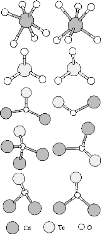
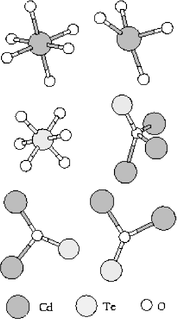
Crystalline CdTeO3 has been obtained in a cubic phase and several monoclinic phases.Kräemer and Brandt (1985); Madelung (1986a) The cubic phase has also been reported in oxidized CdTe.Wang et al. (1987); El Azhari et al. (2000); Arizpe-Chávez et al. (2000); Heiba (2003) Only one of the monoclinic structures has been totally determined.Kräemer and Brandt (1985) This structure belongs to the P2 monoclinic crystallographic class, with the atoms occupying 10 non-equivalent positions. Figure 2 shows the first coordination shell of all the non-equivalent atoms. The structural units are distorted TeO3 trigonal pyramids that are linked to each other with Cd atoms. This arrangement is similar to the one found in tellurite glasses.Ushino and Yoko (1996); Sekiya et al. (1992) There are Cd and Te atoms each of which occupy two non-equivalent sites, and O atoms in six non-equivalent sites. Both Cd atoms are 6-fold coordinated with Cd-O bond lengths in the 2.197-2.476 Å range. The bond angles deviate as much as 31 degrees from the ideal octahedral bond angles of 90 and 180 degrees. O atoms always link one Te atom with one, two, or three Cd atoms, and the average coordination of O atoms is three.
Cd3TeO6 has been recently investigated due to its semiconducting properties and has been proposed as a n-type thermoelectric material.Shan et al. (2002) Its atomic structureBurckhardt et al. (1982) is described as a deformed perovskite-type with pseudo-orthorhombic monoclinic space symmetry P2, 111P2 is a non-standard form of the space group 14, which is the same as the standard P2, except that the lattice vectors and are chosen in such a way that is parallel to the glide translation. Hahm (1983) in which the B-sites are occupied by Cd and Te, and the A-sites by Cd. Adding the oxygen atoms, a total of 6 non-equivalent positions are occupied. The local environments of the non-equivalent atoms are shown in Fig. 3. The first coordination shell of Te atoms is composed of three pairs of O atoms, each pair at a bond length distance of 1.904, 1.924, and 1.948 Å. These lengths lie in the typical range of paratellurite -TeO2 and tellurite glasses.Sekiya et al. (1992); Kowada et al. (1996) Cd atoms occupy two non-equivalent sites. One of them is surrounded by three pairs of O atoms at bond lengths of 2.211, 2.311, and 2.350 Å and bond angles near 90∘. This arrangement is the same as in CdO with rocksalt structure, where the Cd-O bond length at room temperature is 2.344 Å.Madelung (1986b) The other Cd atom is surrounded by four oxygen atoms at 2.237, 2.251, 2.278, and 2.297 Å. Three of these oxygen atoms lie in nearly the same plane as the Cd atom, and the other one lies nearly perpendicular. This complex configuration can be understood as originated by the electrostatic repulsion of the other four O atoms located at 2.596, 2.736, 2.761, and 3.010 Å, which complete a distorted octahedron, but are too far apart to be considered as bound. The O atoms occupy three non-equivalent crystallographic positions and are linked to one Te atom and two or three Cd atoms. The two arrangements of one O atom with two Cd atoms and one Te atom are nearly planar.
The greatest difference between CdTeO3 and Cd3TeO6 is that tellurium atom is 3-fold oxygen coordinated in the first and 6-fold coordinated in the latter. This is due to the fact that the content of tellurium in CdTeO3 is twice that of Cd3TeO6, if CdTeO3 is regarded as Cd2Te2O6. Moreover, the Te octahedral coordination is typical in compounds where Te has degree of oxidation VI.
In summary, in both CdTeO3 and Cd3TeO6, there are only Cd-O and Te-O bonds. Oxygen atoms always bridge one tellurium atom with one, two or three cadmium atoms. In the most typical cases an oxygen atom bridges one Te atom with two Cd atoms, with local quasi-planar arrangement.
III Electronic structure

We have performed calculations of the electronic structure in the framework of the Density Functional Theory (DFT)Hohenberg and Kohn (1964) with the Perdew-ZungerPerdew and Zunger (1981) parametrization of the Local Density Approximation (LDA). The calculations have been performed using the ab-initio total-energy program VASP (Vienna ab-initio simulation program).Kresse and Hafner (1993, 1994); Kresse and Furthmüller (1996a, b) The valence electronic eigenfunctions are obtained from an expansion in plane waves, while the core electrons are replaced by the ultrasoft pseudopotentials supplied in the VASP package. The cutoff of the plane wave expansion depends upon the material composition. We have used the maximal values of the recommended cutoffs of the components: 168, 115, and 396 eV for Cd, Te, and O, respectively.
To obtain a smooth density of states (DOS), the first Brillouin zone has been sampled with k-points generated according to the Monkhorst-Pack scheme. We used grids, with for CdTe, for CdO, for TeO2, for CdTeO3, and for Cd3Te. To eliminate unphysical oscillations in the density of states (DOS) due to the k-space grid, the DOS has been broadened by gaussian functions with 0.2 eV variance. However, for CdTe a broadening of 0.1 eV was used to display the structure of the Cd 4d band. Analyzing the partial DOS we can identify the nature of the peaks observed in the DOS, and correlate the features of the total DOS with the crystal structure. The partial DOS are obtained projecting the electron wave functions onto atomic-like orbitals, and integrating them in atom-centered spheres. The radii of these spheres are the atomic radii times a factor that equals the sum of the volumes of the atomic spheres to the cell volume. Our selection of the atomic radii is discussed in the Appendix.
As a check for the calculations we have performed optimizations of the unit cell volume and the ionic positions of CdTeO3 and CdTe. For CdTeO3, the obtained lattice parameters were 4 % smaller in the LDA than the experimental ones, while the ionic displacements are smaller than 1 % of the lattice parameters. For CdTe, the theoretical lattice constant is 6.43 Å in the LDA, and 6.62 Å in the framework of the Generalized Gradient Approximation (GGA), both being within 2 % of the experimental value 6.481 Å.Madelung (1986b)
As a complement to the band diagram and the partial DOS analysis, we use the electron localization function (ELF)Becke and Edgecombe (1990); Savin et al. (1992); Kohout and Savin (1996); Haussermann et al. (1994) to obtain information on interatomic bonds. The ELF is a measure of the electron localization in space, and helps to visualize the shell structure of atoms and solids. The ELF is defined in terms of the local electronic density , the excess of kinetic energy due to the Pauli exclusion principle , and the Thomas-Fermi kinetic energy density .
| (1) |
In a DFT calculation, and are evaluated from the density and the Kohn-Sham orbitals , as
| (2) | |||||
| (3) |
By definition, ELF values range between 0 and 1. An ELF value close to 1 at a given point indicates a high degree of localization of the electrons at that point. For the homogeneous electron gas, which is used as a reference system in its definition, the ELF is equal to 0.5.
III.1 CdTe
Cadmium telluride is a prototype of II-VI semiconductors. It has the zinc-blende structure, where the anions arrange in a cubic compact structure, and the cations occupy one half of the tetrahedral sites between the anions. The band structure of CdTe was determined 30 years agoChelikowsky et al. (1973); Chelikowsky and Cohen (1976) and has been obtained by ab initio calculation many times (see e.g. Refs. Wei and Zunger, 1988; Yeh et al., 1994; Vogel et al., 1996; Albrecht et al., 1997; Godlevsky et al., 1999). In Fig. 4 we show the DOS. The energies are referred to the valence band maximum. The top valence band (VB) and the bottom conduction band (CB) are mainly composed of Te 5p bonding levels and Cd 5p antibonding levels, respectively. Below the top VB other VBs are placed, originated from the levels Cd 5s, Cd 4d, and Te 5s. It is well documented that LDA predictions of the optical bandgap in II-VI are significantly reduced compared to the experimental values (see Ref. Vogel et al., 1996 and references therein). We have obtained a direct bandgap eV at the point , which is 1.3 eV smaller than the experimental value.222Our calculation does not includes the spin-orbit coupling, which splits the top valence band. Hence, our bandgap must be compared with the average bandgap . Note that the scale of Fig. 4 does not allow one to see the CB edge in the total DOS. LDA also predicts the Cd 4d electron bands to occur about 3 eV higher than the experimental values, but still isolated between Te 5s and Cd 5s bands. This underestimation of the Cd 4d binding energy is due to the unphysical electron self-interaction in Cd 4d orbitals, which is not correctly compensated by the LDA exchange-correlation functional.Wei and Zunger (1988); Vogel et al. (1996) GGA calculations suffer the same shortcoming. However, the topology of the band structure is correctly provided by the LDA calculations. The bandgap underestimation has two sources. One is the error inherent to the LDA exchange-correlation potential, and the other is the discontinuity of the exact DFT exchange correlation potential upon addition of one electron in insulating solids.Perdew and Levy (1983); Sham and Schlüter (1983) Calculations of the exact DFT exchange-correlation potential have shown that nearly 80% of the gap error in Si, GaAs, and AlAs is inherent to exact DFT.Godby et al. (1988) However, the calculation of GaAs in Ref. Godby et al., 1988, which is the most similar case to CdTe, placed the Ga 3d electrons in the Ga frozen core. When the cation d orbitals are treated self-consistently, the unphysical proximity of cation d and anion p bands caused by the self-interaction error repels upwards the higher valence bands, producing a further decrease of the bandgap.

III.2 CdO

CdO is also a II-VI semiconductor. It has rocksalt structure, where the cations are placed in the octahedral interstitials of the close packed anions. As oxygen is more electronegative than tellurium, the Cd-O bonds are more ionic than the Cd-Te ones. The band structure that we have obtained is similar to others obtained within standard LDAVogel et al. (1996) and GGA.Guerrero-Moreno and Takeuchi (2002) Hence, we do not repeat it here. It shows an indirect bandgap, with the valence band maximum (VBM) at point L, and the conduction band minimum (CBM) at point . LDA and GGA erroneously predict a negative bandgap because it improperly accounts for the electron self-interaction in Cd 4d orbitals.Vogel et al. (1996); Guerrero-Moreno and Takeuchi (2002) The unphysical self-interaction in the Cd 4d orbitals raises these levels with respect to the experimental values. The Cd 4d levels repel the upper O 2p levels,Wei and Zunger (1988) thus decreasing the bandgap. This is the same effect that reduces the bandgap in CdTe and other IIB-VIA compounds. However, the structure of the VB here obtained is similar to that calculated using self-interaction- and relaxation-corrected pseudopotentials,Vogel et al. (1996) where the gap problem is corrected and the semiconducting character of CdO is restored.
As can be seen from Fig. 5, the Cd 4d bands are isolated from the top VBs, which in turn are originated from the O 2p levels. Nevertheless, as shown by the partial DOS, there is a certain mixing between O 2p and Cd 4d levels. The mixing of Cd 4d and O 2p levels is the origin of the splitting of the Cd 4d band and the peak at -3.6 eV. 333The partial O 2p character in the Cd 4d band has been proven experimentally in Ref. Smith, 2002 using soft X-ray emission from the O 1s edge. At some points in the Brillouin zone, certain Cd 4d levels have the same symmetry as the O 2p levels and form bonding and antibonding combinations, raising the O 2p levels and lowering the Cd 4d ones.Wei and Zunger (1988) Other Cd 4d levels, at the same or at a different -points, have different symmetry than O 2p levels, and originate the Cd 4d band at higher energy. The DOS shows this effect integrated over the Brillouin zone.
III.3 TeO2

The band structure and the partial DOS of -TeO2 are shown in Figs. 6 and 7. We have obtained an indirect bandgap of 2.768 eV, with the VBM located at points (in fractional units) and the CBM at points , . However, the top VB and the bottom CB are very flat and the direct bandgap =2.851 eV, at is very close to the indirect bandgap. For practical purposes -TeO2 can be considered a direct bandgap material. The flatness of the band edges also indicates a high degree of electron localization. The partial DOS shows that contributions from O 2s and 2p, and Te 5s and 5p orbitals are spread along a wide range of energies, thus indicating that partially covalent bonds are formed. Also, the Te atom contributions to the DOS are one order of magnitude smaller than O atom contributions, indicating a charge transfer from Te atom to O atom.
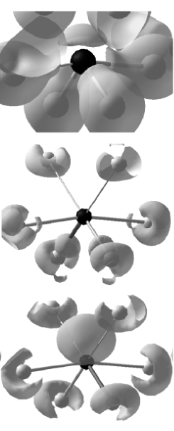
Figure 8 shows an iso-surface of the electronic density and the ELF around a TeO6 cluster inside the crystal structure of -TeO2. The central Te and the four O atoms below it form the above mentioned trigonal bipyramid. Several features should be noted in this figure: (1) directionality of the Te-O bonds in the tbp; (2) a lone pair over the Te atom, opposite to the tbp Te-O bonds; (3) an increment of the charge density around O atoms in the plane perpendicular to the O-Te bonds (this feature confirms the results of cluster calculationsSuehara et al. (1995, 1998)); (4) there are two regions of high electron localization: one over the Te atom, which corresponds to the electrons lone pair, and the other around O atoms in the plane perpendicular to the O-Te bonds. Iso-surfaces for higher ELF (not shown in the figure) concentrate at the Te lone pair. A smaller increment of the charge density ( Å-3) was also found at the Te lone pair region.
III.4 CdTeO3
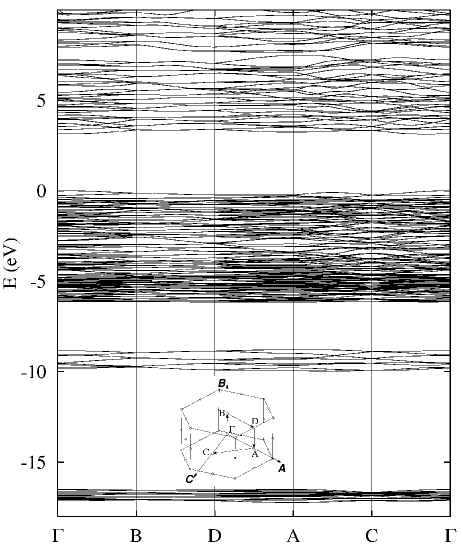
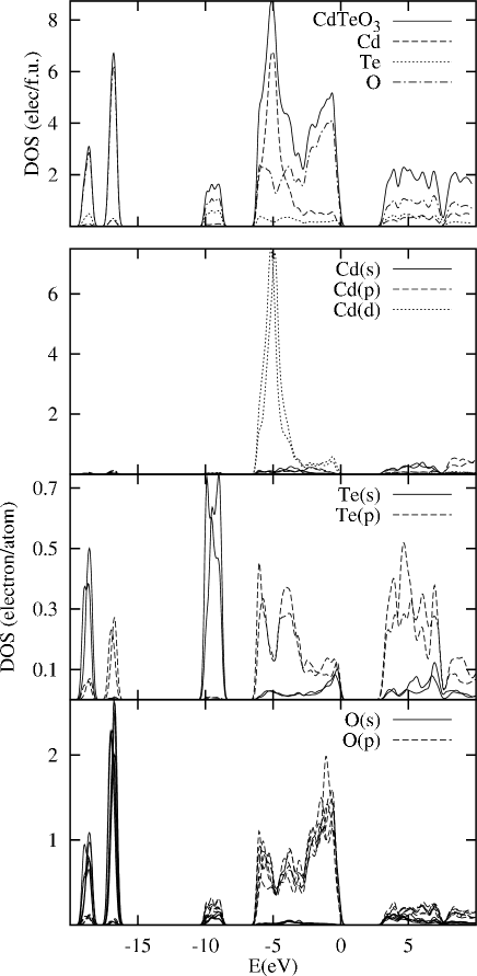
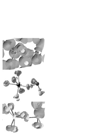

Figure 9 shows the band diagram of CdTeO3. The VBM is located at the point, and the CBM is found at and (in fractional units). Therefore, the bandgap is indirect, with a value =3.028 eV. However, the direct bandgaps eV and eV are very close to the indirect gap. These values are slightly smaller than the experimental value 3.9 eV reported for amorphous nearly stoichiometric CdTeO3 thin films.El Azhari et al. (2000)
The total and partial DOS are shown in Fig. 10. The partial DOS reveals that O 2s orbitals combine with Te 5s and 5p, while O 2p combine with Te 5s and 5p, and Cd 4d orbitals. This indicates a complex electronic structure, the main features of which are: (1) Cd 4d levels concentrate in a single peak in the DOS, with a tail in the region of O 2p levels, and no gap in between; (2) O 2p levels dominate the top VB and also contribute to the lower VBs, being determinant in the O-Te bonds ; (3) Te 5s and Te 5p contributions are distributed throughout the VB, and are very depopulated in benefit of the O 2p levels; (4) the CB edge is dominated by O 2p levels, with contributions from Cd 5s and Te 5p levels. We conclude that the Cd-O bonds have a certain covalent character, expressed in the mixing of the 4d levels of Cd with the 2p levels of O. The ionic character is suggested by the octahedral coordination of Cd, and by the spherical symmetry of the charge distribution around Cd atoms (Fig. 11). However, in contrast to CdO, the partial DOS of CdTeO3 shows that the Cd 4d levels concentrate in one main peak, which is slightly broader than in CdO, and has a background to the higher valence bands without gap. This can be understood as an effect of the more complex atomic environment in this phase with respect to rocksalt-structure CdO. However, the absence of gap between the Cd band and the O 2p band may be caused by the overall tendency of LDA and GGA to underestimate the binding energies and the bandwidths. The Cd 5s levels contribution is present in the conduction band.
Figure 11 shows an iso-surface of the electronic density, the charge density difference (crystalline minus atomic), and the electron localization function (ELF) around a cluster O5Cd-O-TeO2 inside the crystal structure of CdTeO3. Several features should be noted in this image: (1) spherical symmetry of the electronic cloud around the Cd atom; (2) directionality of the Te-O bonds; (3) a lone pair near the Te atom opposite to the Te-O bonds, i.e., over the apex of the pyramid; (4) an increment of the charge density around O atoms in the plane perpendicular to the O-Te bonds (this feature is similar to the case of -TeO2) (5) there are two regions of high electron localization: one over the Te atom, which corresponds to the electron lone pair, and another one around O atoms in the plane perpendicular to the O-Te bonds. Iso-surfaces for higher ELF (not shown in the figure) concentrate at the Te lone pair, as in paratellurite. A smaller charge increment was also found at the Te lone pair region. Note that Å-3 is a rather low density (compare with Fig. 15). For higher values of , the iso-surfaces are nearly atom-centered spheres.
III.5 Cd3TeO6

Figure 12 shows the band diagram of Cd3TeO6. As can be seen, it is an insulator material with a direct bandgap eV at the point. The valence bands are very flat, but the lowest CB shows dispersion and is also isolated from the upper CBs. From the curvature of the conduction band we have estimated an effective mass of 0.2 free electron masses, which is comparable to that of II-VI semiconductors.
The total and partial DOS of Cd3TeO6 are shown in Fig. 13. As in CdTeO3, the top VB is built from Cd 4d and O 2p atomic orbitals, and the lowest VBs are mainly composed of O 2s orbitals with small contributions of Te 5s and 5p orbitals. The bottom CB has contributions from all atoms, the largest of which comes from O 2s and Cd 5s. The most significant difference with CdTeO3 are the triple splitting of the peak associated to O 2s levels between and eV, and the soft CB edge, which is associated to the small effective mass.

We find that the O-Cd bonds are similar to those in the other compounds examined. Te atoms are octahedrally coordinated and transfer about 4 electron charges to neighbor O atoms. The charge density along the line of Te–O bonds is rather similar to the one in CdTeO3, and there is no electron lone pair bond of Te. The electron localization function (not shown here) only points to charge localization around O atoms, which is consistent with the narrow and isolated O 2s bands.
Figure 14 shows comparatively the DOS in all the compound studied here.
IV Discussion
In order to compare our results for the electronic structure of Cd-Te-O compounds, in Table 1 we show a summary of our calculated bandgaps together with previous results.
The electronic structure of CdO is still not well understood due to both theoretical limitations, and experimental facts that obscure its intrinsic properties. On one hand, CdO presents a large defect concentration, which produces carrier concentrations as large as 1020 cm-3,Dou et al. (1997); Wang et al. (2001) a nearly metallic conductivity, a Fermi level inside the conduction band,Dou et al. (1997); Tewari (1973) a blocking of the fundamental absorption edge and a bandgap shrinkage.Dou et al. (1997) To further complicate the interpretation of the optical data, two indirect bandgaps have been observed below the direct bandgap, which are also highly sensitive to the temperature. At the temperature of 100 K the accepted values Koffyberg (1976) for the two indirect bandgaps are 0.84 and 1.09 eV, and for the direct bandgap is 2.28 eV.
Previous band diagram calculations Maschke and Rössler (1968); Breeze and Perkins (1973); Tewari (1973); Boettger and Kunz (1983); Jaffe et al. (1991); Vogel et al. (1996); Dou et al. (1998); Wang et al. (2001); Guerrero-Moreno and Takeuchi (2002) and the present one provide different interpretations for ordering of the indirect bandgaps. Early semi-empirical calculationsBreeze and Perkins (1973); Tewari (1973) and correlated Hartree-Fock self-consistent calculationsBoettger and Kunz (1983); Jaffe et al. (1991) located the VBM at a point, while other semi-empirical,Maschke and Rössler (1968) LDA,Vogel et al. (1996); Dou et al. (1998) periodic Hartree-Fock,Dou et al. (1998) and screened-exchange LDAWang et al. (2001) calculations, as well as this work, locate the VBM at point L. In all cases the energy differences between the valence band maxima at L and at are small. Hartree-Fock calculationsBoettger and Kunz (1983); Jaffe et al. (1991); Dou et al. (1998) overestimate the bandgaps and widths, while LDAVogel et al. (1996); Dou et al. (1998); Wang et al. (2001) and GGAGuerrero-Moreno and Takeuchi (2002) underestimate them. Moreover, the smallest indirect bandgap is negative in some DFT calculations (Refs. Vogel et al., 1996; Guerrero-Moreno and Takeuchi, 2002 and the present one). Although the underestimation of DFT bandgaps is known to be caused by the self-interaction of the Cd 4d levels and the repulsion from the higher levels of the point, it is not easy to assess the reason for the differences between the standard-LDA calculations. A common feature of the negative gap calculations is the use of pseudopotentials (Refs. Vogel et al., 1996 and this work) or supposedly the use of a frozen-core electron configuration.Guerrero-Moreno and Takeuchi (2002) The positions of Cd 4d bands have also been a point of interest. While the early XPS measurement assigned to this band a mean binding energy of 12.8 eVVesely and Langer (1971) with respect to the (undefined) Fermi level, recent measurements have corrected this value to 10.7 eV, or 9.4 eV with respect to the VBM.Dou et al. (1998) The best approximation to this experimental energy up to date is provided by the periodic HF calculation of Ref. Dou et al., 1998. LDA calculations underestimate these binding energies, in this study giving 6.6 eV. Our LDA calculation provides a Cd 4d band splitting equal to 0.9 eV, which agrees with the experimental values of 0.87Vesely and Langer (1971) and 0.8 eV.Scrocco (1991)
| CdTe | |||||||
| Method | Method | Method | |||||
| 1.60 (1.92) | TPAMadelung (1986b)111The value in () is the average of the bands split by the spin-orbit coupling. | 0.3 | PPVogel et al. (1996) | 0.80 | PPZakharov et al. (1994) | ||
| 1.59 | NLPPChelikowsky and Cohen (1976) | 0.8 | SIRC-PPVogel et al. (1996) | 1.76 | PP,GWZakharov et al. (1994) | ||
| 1.44 | LAPWWei and Zunger (1988) | 0.47 (0.79)111The value in () is the average of the bands split by the spin-orbit coupling. | LMTO-RCade and Lee (1985) | ||||
| 0.47 | LAPW-SRWei and Zunger (1988) | 0.51 | LMTO-SRChristensen and Christensen (1986) | ||||
| 0.18 | LAPW-RWei and Zunger (1988) | 0.29 | LMTO-RChristensen and Christensen (1986) | (0.3) 0.573 | PP222The value in () is the estimated correction due to the spin-orbit coupling.333Present calculation. | ||
| CdO | |||||||
| (Cd 4d) | Method | ||||||
| 0.84 | 1.09 | 2.28 | TRKoffyberg (1976) | ||||
| -9.4 | XPSDou et al. (1998) | ||||||
| (Cd 4d) | Method | ||||||
| 0.8 | 1.2 | 2.38 | -6.1 | APWMaschke and Rössler (1968) | |||
| 1.18 | 1.12 | 2.36 | -5.7 | LCAOBreeze and Perkins (1973) | |||
| 1.11 | 0.95 | -4.5 | APWTewari (1973) | ||||
| 6.07 | 6.56 | -12.1 | C-HFJaffe et al. (1991) | ||||
| 10.9 | 11.0 | -13.2 | AE-HFBoettger and Kunz (1983) | ||||
| 0.5 | 0.4 | 0.8 | -14.4 | C-HFBoettger and Kunz (1983) | |||
| -0.6 | -6.2 | PPVogel et al. (1996) | |||||
| 1.7 | 1.7 | 3.4 | -8.2 | SIRC-PPVogel et al. (1996) | |||
| 10.41 | 10.44 | 11.66 | -10.3 | AE-HFDou et al. (1998) | |||
| 0.39 | 0.47 | 1.61 | -7.1 | AE-LDADou et al. (1998) | |||
| 2.36 | sx-LDAWang et al. (2001) | ||||||
| -0.5 | 0.7 | -6.5 | LAPW-GGAGuerrero-Moreno and Takeuchi (2002) | ||||
| -0.465 | -0.386 | 0.712 | -6.6 | PP333Present calculation. | |||
| TeO2 | CdTeO3 | Cd3TeO6 | |||||
| Method | Method | Method | Method | ||||
| 3.6-3.9 | OPAUchida (1971) | 1.7 () | LCAORobertson (1979) | 3.9 | OPAEl Azhari et al. (2000)444In amorphous thin films. | 1.7 | guess555Theoretical value plus 1 eV, following the overall trend. |
| 4.2 (dir) | OPAMansingh and Kumar (1988)444In amorphous thin films. | 1.9 () | LCAORobertson (1979) | ||||
| 3.75 (ind) | OPAMansingh and Kumar (1988)444In amorphous thin films. | 2.768 () | PP333Present calculation. | ||||
| 0 | LMTO-SRSvane and Antoncik (1987) | 2.846 () | PP333Present calculation. | 3.028 | PP333Present calculation. | 0.714 | PP333Present calculation. |
TPA: Two-photon absorption at T=4.2 K.
OPA: One photon absorption at room temperature.
TR: Thermoreflectance at T=100 K.
PP: Self-consistent LDA with pseudopotentials, which include scalar relativistic effects.
NLPP: Empirical non-local pseudopotentials.
LAPW: Self-consistent LDA linearized augmented plane waves.
LMTO: Self-consistent LDA linearized muffin-tin orbital.
NR: No relativistic, SR: Scalar-relativistic (without spin-orbit coupling), R: Relativistic.
AE: All electrons calculation.
SIRC-PP: Self-consistent LDA with self-interaction and relaxation corrected pseudopotentials.
APW: Non-self-consistent augmented plane waves.
LCAO: Empirical linear combination of atomic orbitals.
C-HF: All electrons correlated Hartree-Fock.
sx-LDA: Screened-exchange LDA.
The electronic structure of -TeO2 provided by our calculation is compared in the following with previous findings. The band diagram of idealized TeO2 with rutile structure has been calculated using the empirical tight-binding methodRobertson (1979) and the scalar-relativistic linear muffin-tin LDA method.Svane and Antoncik (1987) Both calculations show important differences in the DOS, particularly the self-consistent one,Svane and Antoncik (1987) where a metallic band structure was obtained. We performed a test calculation with the structure of rutile and we also found a metallic DOS. The failure of the rutile model of TeO2 is due to the asymmetry of the Te-O bonds in the first coordination shell of Te in the paratellurite structure, as has been demonstrated in clusters calculationsSuehara et al. (1994, 1995, 1998) and in our results. An XPS spectra was reported and interpreted with the help of a self-consistent-charge discrete variational X calculation of TeO6 clusters.Suehara et al. (1994) Our findings of the crystal electronic structure calculation support this interpretation and our DOS corresponds fairly well with the discrete levels of the clusters. The most significant difference is the existence of a double peak centered at eV and eV in our DOS, which is composed of mixed Te 5s and O 2p orbitals. This feature corresponds to the band C of Ref. Suehara et al., 1994, which is not split in the calculations nor in the observed XPS spectrum. Berthereau et alBerthereau et al. (1996) have reported Hartree-Fock calculations of charged clusters TeO, which predict the higher occupied molecular orbital (HOMO) to be antibonding and composed of mixed Te 5s-O 2p orbitals and have suggested that this molecular orbital corresponds to the Te lone pair. This level can be correlated to the conduction band edge predicted by our crystal calculation. The crystal calculation is more consistent with less-charged clusters, where the HOMO of Berthereaud et al becomes the lowest unoccupied molecular orbital, and the HOMO is composed of non-bonding O 2p levels,Berthereau et al. (1996) in correspondence with our valence band edge. Based on their study of charged TeO clusters, Suehara et alSuehara et al. (1995) estimated the net charge of the TeO6 structural unit to be , and the net charge of Te atoms to be , This coincides closely with our estimation based on ab-initio atomic radii (see Appendix). The optical bandgap provided by our LDA calculation near 2.8 eV can be compared with available data. UchidaUchida (1971) measured the absorption in the pre-edge region, in which an Urbach tail behavior can be observed. Although no attempt was made to estimate a direct or indirect gap, it is clear from their spectra that the fundamental edge of paratellurite lies in the region 3.6-3.9 eV. Mansingh and KumarMansingh and Kumar (1988) measured the optical properties of TeO2 thin films prepared by vacuum evaporation and found an indirect gap at 3.75 eV and a direct gap at 4.2 eV related to a strong absorption. Although it is not clear if their as-grown films were amorphous or polycrystalline, these values provide an indication of the bandgap for ideal crystals. Hence, the LDA calculation underestimates the paratellurite bandgap by approximately 1 eV.
The theoretical electronic properties of CdTeO3 and Cd3TeO6 can be discussed only with reference to amorphous thin films or oxidized CdTe crystals, as there is no data for crystalline CdTeO3 and Cd3TeO6. The bandgap of nearly stoichiometric amorphous CdTeO3 is 3.9 eV.El Azhari et al. (2000) Hence, LDA underestimates the bandgap in 0.9 eV, which is the same trend as in TeO2, CdO, and CdTe. Based on this trend we predict a bandgap around 1.7 eV for Cd3TeO6. This material has recently been found to be semiconducting and susceptible to n-doping.Shan et al. (2002) These experimental findings are in agreement with our predicted gap, conduction band and effective mass.
Our final comment is devoted to the spin-orbit coupling, which is known to have a significant effect on the bandgaps of M-Te compounds (M=Zn,Cd,Hg) (see e.g. Ref. Wei and Zunger, 1988). The spin-orbit splitting of the fundamental bandgap of these compounds arises mostly from the Te 5p orbitals. As our calculation does not include this effect, our calculated gaps should be regarded as averaged values. However, in the compounds other than CdTe the partial DOS of Te 5p levels is largely reduced, and the O 2s and O 2p orbitals give the greatest contributions to the DOS. Hence, we expect that the spin-orbit effects on the bandgap should be much smaller than in CdTe. However, calculations with the spin-orbit coupling included could be needed in case that precise measurements of the band properties were produced.
Acknowledgements.
This work has been supported by FONDECYT (Chile) grants 7030083 and 1030063, Alma Mater grant 32-2000 (Havana University) and a fellowship from the Third World Academy of Sciences. We also thank S. Davis for computer assistance. E. M-P also thanks P. Ordejon, E. Artacho, and A. R. Ruiz-Salvador for many useful suggestions.Appendix A Determination of the atomic radii

To obtain the partial DOS it is necessary to define atomic spheres for the integration of the local DOS. The atomic radii cannot be unambiguously defined, being just measures of their spatial extension, and depend on the environment. Partial atomic charges can be obtained by integration of the partial atomic DOS up to the Fermi level. These partial charges have no exact meaning, but can be used as a reference to compare the chemical bonds in the different compounds.
| Cd | Te | O | ||||
| Compound | (Å) | (Å) | q | (Å) | q | |
| CdTe (C) | 1.48 | 1.35 | +0.46 | |||
| (A) | 1.29 | +0.46 | 1.52 | |||
| CdO (I) | 1.09 | +1.6 | 1.28 | |||
| (A) | 1.20 | +1.1 | 1.14 | |||
| TeO2(I) | 0.80 | +4.4 | 1.24 | |||
| (A) | 0.9 | +3.1 | 1.10 | |||
| CdTeO3(I) | 1.09 | 1.45 | 0.80 | +4.42 | 1.24 | |
| (C) | 1.48 | 1.35 | 0.73 | +0.57 | ||
| (A) | 1.23 | +0.7 | 0.9 | +3.3 | 1.10 | |
| Cd3TeO6(I) | 1.09 | +1.6 | 0.70 | +5.6 | 1.24 | |
| (A) | 1.23 | +0.97 | 0.90 | +3.95 | 1.1 | |
Usually, tabulated covalent and ionic radii are employed for the partial DOS calculations (see Table 2). Additionally, we have obtained ab-initio radii analyzing the density of charge along the bonds. Figure 15 shows the electronic pseudocharge density along the bond directions for all types of bonds present in the Cd-Te-O system. It can be noticed the difference between the Cd-O, Cd-Te and Te-O bonds. While the Cd-Te and Cd-O bonds show clear interatomic regions with minimal charge density, the Te-O bond shows an intermixing of the atomic electron bonds. For Cd-O and Cd-Te bonds, we estimated the atomic radius as the distance between the nucleus and the minimum of the valence electron density along the bond. In the case of Te-O bonds, the electronic density grows continuously from Te to O. Hence we set the Te-O boundary at the point where the second derivatives is null. As several distances exist in materials other than CdTe and CdO, we averaged the obtained atomic radii. Table 2 shows the atomic charges assuming these ab-initio radii, as well as ionic and covalent radii. As can be seen, with the covalent radii, the atomic charges in CdTe and CdTeO3 have wrong sign. This is rather unexpected in CdTe, where the bond length is well approximated by the sum of the covalent radii of Cd atom and Te atom. Using the ionic radii, the charges in TeO2, CdTeO3, and Cd3TeO6 are in better agreement from values obtained from a chemical point of view, but the charge of Te atom is extremely high, and O appears over-ionized in TeO2. In this sense, the charges estimated with the ab-initio radii seem undoubtedly more reasonable. The change observed in the partial DOS calculated with different atomic radii is fundamentally a scale factor.
References
- Zanio (1978) K. Zanio, in Cadmium Telluride, edited by P. K. Willardson and A. C. Beer (Academic, New York, 1978), vol. 14 of Semiconductors and Semimetals.
- Espinoza-Beltrán et al. (1991) F. J. Espinoza-Beltrán, F. Sánchez-Sinencio, O. Zelaya-Angel, J. G. Mendoza-Álvarez, C. Alejo-Armenta, C. Vázquez-López, M. H. Farias, G. Soto, L. Cota-Araiza, J. L. Peña, et al., Jpn. J. Appl. Phys. 30, L1717 (1991).
- Espinoza-Beltrán et al. (1993) F. J. Espinoza-Beltrán, O. Zelaya, F. Sánchez-Sinencio, J. G. Mendoza-Álvarez, M. H. Farias, and L. Baños, J. Vac. Sci Technol. A 11, 3062 (1993).
- Zapata-Navarro et al. (1994) A. Zapata-Navarro, M. Zapata-Torres, V. Sosa, P. Bartolo-Pérez, and J. L. Peña, J. Vac. Sci. Technol. A 12, 714 (1994).
- Zapata-Navarro et al. (1997) A. Zapata-Navarro, P. Bartolo-Pérez, M. Zapata-Torres, R. Castro-Rodríguez, and J. L. Peña, J. Vac. Sci. Technol. A 15, 2537 (1997).
- El Azhari et al. (1997) M. Y. El Azhari, M. Azizan, A. Benouna, A. Outzourhit, E. Ameziane, and M. Brunel, Thin Solid Films 295, 131 (1997).
- Bartolo-Pérez et al. (1999) P. Bartolo-Pérez, J. L. Peña, and M. H. Farias, Sup. Vac. 8, 59 (1999).
- Caballero-Briones et al. (1998) F. Caballero-Briones, A. Zapata-Navarro, P. Bartolo-Pérez, R. C. Rodríguez, M. Zapata-Torres, W. Cauich, and J. L. Peña, Rev. Mex. Fis. 44 Supl. 3, 268 (1998).
- Iribarren et al. (1999) A. Iribarren, E. Menéndez-Proupin, F. Caballero-Briones, R. Castro-Rodriguez, and J. L. Peña, J. Appl. Phys. 86, 4668 (1999).
- Arizpe-Chávez et al. (2000) H. Arizpe-Chávez, R. Ramírez-Bon, F. Espinoza-Beltrán, O. Zelaya-Angel, J. Marín, and R. Riera, J. Phys. Chem. Solids 61, 511 (2000).
- Iribarren et al. (2001) A. Iribarren, E. Menéndez-Proupin, F. Caballero-Briones, R. Castro-Rodriguez, and J. L. Peña, Mod. Phys. Lett. B 15, 643 (2001).
- Bartolo-Pérez et al. (2002a) P. Bartolo-Pérez, R. C. Rodríguez, F. Caballero-Briones, W. Cauich, J. L. Peña, and M. H. Farias, Surf. Coat. Technol. 155, 16 (2002a).
- Bartolo-Pérez et al. (2002b) P. Bartolo-Pérez, J. Ceh, J. L. Peña, A. Zapata-Navarro, and M. H. Farias, Sup. Vac. 15, 30 (2002b).
- Ebina et al. (1980) A. Ebina, K. Asano, and T. Takahashi, Phys. Rev. B 22, 1980 (1980).
- Davis et al. (1981) G. D. Davis, T. S. Sun, S. P. Buchner, and N. E. Byer, J. Vac. Sci. Technol. 19, 472 (1981).
- Wang et al. (1987) F. Wang, A. Schwartzman, A. L. Fahrenbruch, R. Sinclair, R. H. Bube, and C. M. Stahle, J. Appl. Phys 62, 1469 (1987).
- Choi and Lucovsky (1988) S. S. Choi and G. Lucovsky, J. Vac. Sci. Technol. B 6, 1198 (1988).
- Heiba (2003) Z. K. Heiba, Cryst. Res. Technol. 38, 488 (2003).
- Miotto et al. (2003) R. Miotto, F. D. Kiss, and A. C. Ferraz, Surf. Sci. 525, 24 (2003).
- Wei and Zunger (1988) S.-H. Wei and A. Zunger, Phys. Rev. B 37, 8958 (1988).
- Vogel et al. (1995) D. Vogel, P. Krüger, and J. Pollmann, Phys. Rev. B 52, R14316 (1995).
- Vogel et al. (1996) D. Vogel, P. Krüger, and J. Pollmann, Phys. Rev. B 54, 5495 (1996).
- Albrecht et al. (1997) M. Albrecht, B. Paulus, and H. Stoll, Phys. Rev. B 56, 7339 (1997).
- Godlevsky et al. (1999) V. V. Godlevsky, M. Jain, J. J. Derby, and J. R. Chelikowsky, Phys. Rev. B 60, 8640 (1999).
- Boettger and Kunz (1983) J. C. Boettger and A. B. Kunz, Phys. Rev. B 27, 1359 (1983).
- Jaffe et al. (1991) J. E. Jaffe, R. Pandey, and A. B. Kunz, Phys. Rev. B 43, 14030 (1991).
- Dou et al. (1998) Y. Dou, R. G. Egdell, D. S. L. Law, N. M. Harrison, and B. G. Searle, J. Phys.: Condens. Matter 10, 8447 (1998).
- Wang et al. (2001) A. Wang, J. R. Babcock, N. L. Edleman, A. W. Metz, M. A. Lane, R. Asahi, V. P. Dravid, C. R. Kannewurf, A. J. Freeman, and T. J. Marks, PNAS 98, 7113 (2001).
- Guerrero-Moreno and Takeuchi (2002) R. J. Guerrero-Moreno and N. Takeuchi, Phys. Rev. B 66, 205205 (2002).
- Kowada et al. (1996) Y. Kowada, K. Morimoto, H. Adachi, M. Tatsumisago, and T. Minami, J. Non-Cryst. Solids 144, 204 (1996).
- Ushino and Yoko (1996) T. Ushino and T. Yoko, J. Non-Cryst. Solids 204, 243 (1996).
- Suehara et al. (1994) S. Suehara, K. Yamamoto, S. Hishita, and A. Nukui, Phys. Rev. B 50, 7981 (1994).
- Suehara et al. (1995) S. Suehara, K. Yamamoto, S. Hishita, T. Aizawa, S. Inoue, and A. Nukui, Phys. Rev. B 51, 14919 (1995).
- Berthereau et al. (1996) A. Berthereau, E. Fargin, A. Villezusanne, R. Olazcuaga, G. L. Flem, and L. Ducasse, J. Solid State Chem. 126, 143 (1996).
- Suehara et al. (1998) S. Suehara, S. Hishita, S. Inoue, and A. Nukui, Phys. Rev. B 58, 14124 (1998).
- Yakovlev et al. (2002) D. S. Yakovlev, A. P. Mirgorodski , A. Tulub, and B. F. Shchegolev, Opt. Spectrosc. 92, 449 (2002).
- Thomas (1988) P. A. Thomas, J. Phys. C.: Solid State Phys. 21, 4611 (1988).
- Madelung (1986a) O. Madelung, ed., Landolt-Börnstein Numerical Data and Functional Relationships in Science and Technology, vol. III/7b (Springer, Berlin, 1986a).
- Burckhardt et al. (1982) V. H.-G. Burckhardt, C. Platte, and M. Trömel, Acta Cryst. B 38, 2450 (1982).
- Kräemer and Brandt (1985) V. Kräemer and G. Brandt, Acta Cryst. C 41, 1152 (1985).
- Kokalj (1999) A. Kokalj, J. Mol. Graphics Modelling 17, 176 (1999).
- Kokalj and Causa (2000) A. Kokalj and M. Causa, in Proceedings of High Performance Graphics Systems and Applications European Workshop (Bologna, 2000), pp. 51–54.
- Berndt (1997) M. Berndt, ICSD retrieve 2.01, Gmelin Institute, FIZ, Karlsruhe (1997).
- Mackay and Mackay (1969) K. M. Mackay and R. A. Mackay, Introduction to Modern Inorganic Chemistry (Intertext Books, London, 1969), p. 148.
- Robertson (1979) J. Robertson, J. Phys. C: Solid State Phys. 12, 4767 (1979).
- Svane and Antoncik (1987) A. Svane and E. Antoncik, J. Phys. Chem. Solids 48, 171 (1987).
- Mirgorodsky et al. (2000) A. Mirgorodsky, T. Merle-Méjean, J.-C. Champarnaud, P. Thomas, and B. Frit, J. Phys. Chem. Solids 61, 501 (2000).
- El Azhari et al. (2000) M. Y. El Azhari, M. Azizan, A. Bennouna, A. Outzourhit, E. Ameziane, and M. Brunel, Thin Solid Films 366, 82 (2000).
- Sekiya et al. (1992) T. Sekiya, N. Mochida, A. Oshtsuka, and M. Tonokawa, J. Non-Cryst. Solids 144, 128 (1992).
- Shan et al. (2002) Y. J. Shan, K. Sasaki, K. Sudo, H. Imoto, and M. Itoh, Jpn. J. Appl. Phys. Pt. 2 41, L780 (2002).
- Madelung (1986b) O. Madelung, ed., Landolt-Börnstein Numerical Data and Functional Relationships in Science and Technology, vol. III/22 (Springer, Berlin, 1986b).
- Hohenberg and Kohn (1964) P. Hohenberg and W. Kohn, Phys. Rev. 136, B864 (1964).
- Perdew and Zunger (1981) J. P. Perdew and A. Zunger, Phys. Rev. B 23, 5048 (1981).
- Kresse and Hafner (1993) G. Kresse and J. Hafner, Phys. Rev. B 47, 558 (1993).
- Kresse and Hafner (1994) G. Kresse and J. Hafner, Phys. Rev. B 49, 14251 (1994).
- Kresse and Furthmüller (1996a) G. Kresse and J. Furthmüller, Comput. Mat. Sci. 6, 15 (1996a).
- Kresse and Furthmüller (1996b) G. Kresse and J. Furthmüller, Phys. Rev. B 54, 11169 (1996b).
- Becke and Edgecombe (1990) A. D. Becke and K. E. Edgecombe, J. Chem. Phys. 92, 5397 (1990).
- Savin et al. (1992) A. Savin, O. Jepsen, J. Flad, O. Andersen, H. Preuss, and H. G. von Schnering, Angew. Chem. Int. Ed. Engl. 31, 187 (1992).
- Kohout and Savin (1996) M. Kohout and A. Savin, Int. J. Quantum Chem. 60, 875 (1996).
- Haussermann et al. (1994) U. Haussermann, S. Wengert, P. Hofmann, A. Savin, O. Jepsen, and R. Nesper, Angew. Chem. Int. Ed. Engl. 33, 2069 (1994).
- Chelikowsky et al. (1973) J. Chelikowsky, D. J. Chadi, and M. L. Cohen, Phys. Rev. B 8, 2786 (1973).
- Chelikowsky and Cohen (1976) J. R. Chelikowsky and M. L. Cohen, Phys. Rev. B 14, 556 (1976).
- Yeh et al. (1994) C.-Y. Yeh, S.-H. Wei, and A. Zunger, Phys. Rev. B 50, 2715 (1994).
- Perdew and Levy (1983) J. P. Perdew and M. Levy, Phys. Rev. Lett. 51, 1884 (1983).
- Sham and Schlüter (1983) L. J. Sham and M. Schlüter, Phys. Rev. Lett. 51, 1888 (1983).
- Godby et al. (1988) R. W. Godby, M. Schlüter, and L. J. Sham, Phys. Rev. B 37, 10159 (1988).
- Dou et al. (1997) Y. Dou, T. Fishlock, R. G. Egdell, D. S. L. Law, and G. Beamson, Phys. Rev. B 55, R13381 (1997).
- Tewari (1973) S. Tewari, Solid State Commun. 12, 437 (1973).
- Koffyberg (1976) F. P. Koffyberg, Phys. Rev. B 13, 4470 (1976).
- Maschke and Rössler (1968) K. Maschke and U. Rössler, Phys. Status Solidi 28, 577 (1968).
- Breeze and Perkins (1973) A. Breeze and P. Perkins, Solid State Commun. 13, 1031 (1973).
- Vesely and Langer (1971) C. J. Vesely and D. W. Langer, Phys. Rev. B 4, 451 (1971).
- Scrocco (1991) M. Scrocco, J. Electron Spectrosc. Relat. Phen. 53, 225 (1991).
- Christensen and Christensen (1986) N. E. Christensen and O. B. Christensen, Phys. Rev. B 33, 4739 (1986).
- Zakharov et al. (1994) O. Zakharov, A. Rubio, X. Blase, M. L. Cohen, and S. G. Louie, Phys. Rev. B 50, 10780 (1994).
- Cade and Lee (1985) N. A. Cade and P. M. Lee, Solid Stat. Commun. 56, 637 (1985).
- Uchida (1971) N. Uchida, Phys. Rev. B 4, 3736 (1971).
- Mansingh and Kumar (1988) A. Mansingh and S. Kumar, Thin Solid Films 161, 101 (1988).
- (80) Source: Web Elements [http://www.webelements.com/].
- Shannon (1976) R. D. Shannon, Acta Cryst. A 32, 751 (1976).
- Hahm (1983) T. Hahm, ed., International Tables of Crystallography (The International Union of Crystallography. D. Reidel Publishing Company, Dordrecht, 1983).
- Smith (2002) K. E. Smith, Solid State Sci. 4, 359 (2002).