Charge redistribution between cyclotron-resolved edge states at high imbalance
Abstract
We use a quasi-Corbino sample geometry with independent contacts to different edge states in the quantum Hall effect regime to investigate a charge redistribution between cyclotron-split edge states at high imbalance. We also modify Büttiker formalism by introducing local transport characteristics in it and use this modified Büttiker picture to describe the experimental results. We find that charge transfer between cyclotron-split edge states at high imbalance can be described by a single parameter, which is a transferred between edge states portion of the available for transfer part of the electrochemical potential imbalance. This parameter is found to be independent of the particular sample characteristics, describing fundamental properties of the inter-edge-state scattering. From the experiment we obtain it in the dependence on the voltage imbalance between edge states and propose a qualitative explanation to the experimental findings.
pacs:
73.40.Qv 71.30.+hJust from the beginning of the quantum Hall investigations it was understood that edge states play a significant role in many transport phenomena in the quantum Hall effect regime halperin . In a quantizing magnetic field the edge potential bends up the energy levels near the sample edges. At the intersections of the energy levels with Fermi level edge states are formed. It was a paper of Büttiker buttiker that proposes a formalism for the Hall resistance calculation regarding a transport through edge states. This model was further developed by Chklovskii et al. shklovsky for electrostatically interacting electrons. The interaction modifies one-dimentional Büttiker edge states into the stripes of incompressible electron liquid of finite widths. It was shown theoretically buttiker and confirmed in experiments haug that quantum Hall resistance is not sensitive to the inter-edge-channel scattering. Nevertheless, the properties of this scattering can be investigated by using the selective edge channel population methods.
Most of experiments have been performed in the Hall-bar geometry by using the cross gate technique haug . These experiments have revealed the inter-edge-scattering dependence on the magnetic field, temperature and filling factor haug . In the Hall-bar geometry the experiments are at low imbalance conditions, when the energy difference between edge states is smaller than the spectral gaps. An attempt to increase the edge states imbalance by closing cross-gates dramatically decreases the experimental accuracy, as it was mentioned in Ref. muller, .
Another experimental method is the using of the quasi-Corbino sample geometry weiss ; alida . In this geometry two not-connecting etched edges are formed in the sample. A cross-gate is used to redirect some edge states between etched edges and to define an interaction region at one edge. Because the interacting edge states originate from different edges of the sample, they are independently contacted and direct inter-edge-scattering investigations become possible at any imbalance between edge states. This imbalance is controlled by the applied voltage, and in dependence of it’s sign the edge potential profile between edge states becomes stronger of flatter. In the later case at some voltage imbalance the potential barrier between edge states disappears, leading to a step-like behavior of the corresponding branch of the curve. This effect opens a path to use the quasi-Corbino geometry for spectroscopical investigations at the sample edge. Recently, the quasi-Corbino geometry was used to investigate the edge spectrum of single-alida and double-dqwedge layer two-dimensional electron structures. It was also understood that in the transport between spin-resolved edge states at high imbalance (i.e. higher than the spectral gaps) nuclear effects become important DNP .
When developed, Büttiker formalism was intended to describe a high accuracy of the sample resistance quantization in the quantum Hall effect regime. For this reason, it depicts the inter-edge scattering by integral sample characteristics, practically as scattering between ohmic contacts. This picture becomes inconvenient while describing a charge transfer between edge states at high imbalance, where the scattering by definition takes place on small lengths, much smaller than the sample size.
Here, we investigate a charge transfer between cyclotron-split edge states at high imbalance. We modify Büttiker formalism by introducing local transport characteristics in it. We find that charge transfer can be described by a single parameter, which is the transferred portion of the available for the transfer part of the electrochemical potential imbalance. This modified Büttiker picture is used to describe details of charge transfer while current is overflowing between edge channels.
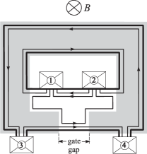
Our samples are fabricated from a molecular beam epitactically-grown GaAs/AlGaAs heterostructure. It contains a two-dimensional electron gas (2DEG) located 70 nm below the surface. The mobility at 4K is 800 000 cm2/Vs and the carrier density 3.7 cm-2. Samples are patterned in a quasi-Corbino geometry alida , see Fig. 1. Rectangular mesa has an etched region inside. Ohmic contacts are made to both (inner and outer) edges of the sample. A Shottky gate is patterned around the inner etched area, leaving uncovered T-shaped region between inner and outer edges. This region forms a narrow (about several microns) strip of uncovered 2DEG near the outer edge of the sample which is called gate-gap. Here we present data from the sample with m gate-gap width, while m gate-gap samples are also investigated showing identical experimental results.
In our experimental set-up one of the inner contacts is always grounded. In a quantizing magnetic field, at filling factors , we deplete 2DEG under the gate to a smaller filling factor , redirecting cyclotron-split edge states from inner to outer edges of the sample. We apply a dc current to one of the outer contacts and measure a dc voltage drop between two others inner and outer contacts at the temperature of 30 mK. By switching current and voltage contacts traces for four different contact combinations can be investigated. Because of independent ohmic contacts to the cyclotron-split edge states, the measured voltage is connected to the voltage drop between edge states in the gate-gap, which is directly the energy shift between them. For example, for contact combination at which contacts no. 4 and 2 are current contacts and no. 3 and 1 are voltage ones, as denoted in Fig. 1.
Examples of experimental curves are presented in insets to Figs. 2,3 for two groups of cyclotron-split edge states. While increasing a current from zero to positive values, the measured voltage rising abruptly to a some value . It is practically no current before , but after it the voltage is a roughly linear function of the current. This linear law is valid for hundreds of nanoAms, see main Figs. 2,3, up to our highest applied currents for filling factor combination . For at high currents there is a strong deviation from the linear law. The deviation starts from twice the onset voltage , and leads to increasing the resistance in respect to the linear dependence. It can not be due to overheating the sample by the current because it would diminish the resistance, in contradiction with the experiment, see Fig. 3.
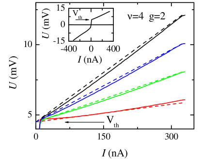
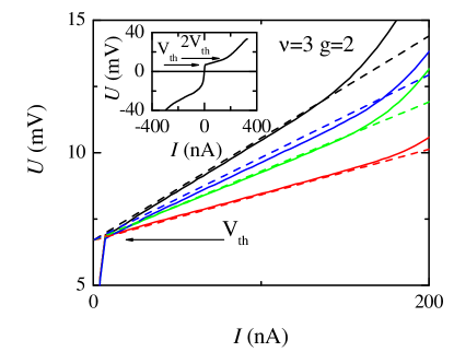
In Figs. 2,3 positive branches are shown for four different contact combinations. As it can be seen from the figure, there is still small non-linearity of the curves. The described above behavior is valid for all of them and is very reproducible from sample to sample and in cooling cycles. Positive branches start from the same threshold voltage, which is fixed for a given filling factor combination. The threshold voltage values are close to the cyclotron splitting in the corresponding field, but smaller on approximately 2 mV, see Ref. alida, : mV for ( meV) and mV for ( meV).
While sweeping the current to the negative values, there is no a clear defined onset: the voltage is rising with rising the current practically from a zero value. The negative branch of the curve is clearly non-linear for any currents, see insets to Figs. 2,3. The exact form of the branch is dependent on the cooling procedure and may variate from cycle to cycle.
To be correct, Büttiker formalism buttiker can not be conveniently applied to the transport at high imbalance. It describes integral sample resistance, so in the case of non-linear curve the Büttiker transmission coefficients become to be dependent on the voltage imbalance between edge states.
As an example, let us consider a filling factor combination . Our sample can be described by the equations buttiker :
| (1) |
where is the current flowing in the -th contact, is the electrochemical potential of the -th contact, and is the matrix of transmission coefficients buttiker . This coefficients are not independent: because of the charge conservation in the gate-gap we can write
| (2) |
Also from symmetry considerations we should mention that
It means that every transmission coefficient can be expressed through a single value, which we define as .
Let the current flow between contacts no. 4 and 1, and use the contacts no. 3 and 2 to measure the voltage drop. For these experimental conditions the flowing current is and there is no current in the voltage probes . Also the voltage drop is a difference of the electrochemical potentials of the potential contacts,so . By solving a system (1) with relations (2) and herein we can obtain
| (3) |
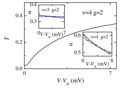
The relation (3) can be used to calculate from the experimental trace, see Fig. 4. The dependence is strongly non-linear. It starts from the threshold voltage, because below threshold practically no current is flowing so the transmission is practically zero. While increasing the voltage imbalance between edge states , is monotonically rising and asymptotically trends to the equilibrium Büttiker value at high voltages . dependance has a universal character: while obtained, it can be used to describe the experimental traces for any given contact combination at fixed filling factors. One should calculate the current-voltage relation for this contact combination from Eq. (1) and introduce the found above into it to obtain the experimental curve. We will demonstrate this fact below in a physically more transparent manner.
Using strongly non-linear transparency is too sophisticated to analyze the overflowing current at , e.g. it is not clear the physical origin of the linear regions on the experimental curves. For the non-linear transport in the gate-gap it is obvious to introduce local transport characteristics instead of the integral Büttiker transmission coefficient . From the positive branch of the experimental curve we conclude that there is practically no current between edge states below the threshold voltage. In Büttiker picture of edge states it means that both edge states are injecting and leaving the gate-gap region with their own electrochemical potentials and , originating from corresponding ohmic contacts no. 1 and no. 3. Currents, flowing in the gate-gap are equal to and in the inner and outer edge states correspondingly. A current between edge states starts to flow then the difference in electrochemical potentials exceeds the threshold voltage. In the other words, only some part of the incoming electrochemical imbalance is available for redistribution between edge states. It is obvious in this case to describe the current between edge states as , where is a parameter, describing a portion of the available part of electrochemical potential imbalance, which is in fact transferred between edge states. For the described above filling factor combination it is clear that means equal redistribution between edge states. The edge states are leaving the gate-gap region with mixed electrochemical potentials and . By introducing these values into the Büttiker formulas (1) we have the following equations instead of (1-3):
| (4) |
In this case there is no need in any additional relations (all the necessary information is indeed in the equations (4)) and the only parameter has a clear physical sense: it is a transferred between edge states portion of the available for the transfer part of the electrochemical potential imbalance between edge states. The above mentioned combination of filling factors and contacts can be described by relation
| (5) |
It is important to mention that because is the local characteristic of the inter-edge state transport it should be independent from the contact combination. In other words, a single value of obtained from different curves is a test of the consistency of our description.
The linear behavior of experimental curves after the threshold means a constant slope in Eq. (5) and, therefore, a constant . In Figs. 2,3 the linear regions of experimental curves are fitted by dashed lines. These lines are calculated from formulas like Eq. (5) with constant single for every filling factor combination. The used values of are for factors and for . It can be seen from the figures, that dashed lines fit the experimental curves quite well, even in view of small non-linearity of the experimental curves. The same values of were obtained from similar linear fits for other samples with different gate-gap widths. We should conclude, that depends only on the filling factor combination and therefore describe fundamental properties of the inter-edge-state transport.
The fact that the experimental traces are not exactly linear, see Figs. 2,3, indicates that there is a slow dependence of on the voltage imbalance between edge states. Using formulas like Eq. (5) it is possible to extract this dependence of directly from the experimental traces. In the insets to Fig. 4 the dependence of is depicted as function of the voltage imbalance between edge states for two different filling factor combinations. Just from the definition is zero before the threshold, it jumps to the values that close but slightly higher than ones for full equilibration between all involved edge states ( for filling factors and for ) and then slowly diminishing while increasing the voltage imbalance between edge states. For a single filling factor combination traces obtained from different contact configurations deviate within 2% which is of the order of our experimental accuracy, which also indicates the universal character of the parameter.
Let us discuss the obtained dependence of on voltage imbalance between edge states, see insets to Fig.4. It is important to mention that by definition describes the resulting mixing of the electrochemical potentials, while charge transfer is taking place on the whole length of the gate-gap width. This charge transfer is changing the electrochemical potentials of the edge states. It means that while at one (injection) corner of the gate-gap the energy shift between edge states equals to the depicted in the figures voltage imbalance between them, the edge potential profile between edge states is flattening while moving away from the injection corner. At some point the edge profile becomes to be flat. If this point is really within the gate-gap, full equilibration between edge states is established, and it should be no further charge transfer on the rest of the gate-gap width. The resulting value of in this case can be expected to be exactly equal to the equilibrium one. The experimental fact that the values of are higher than the equilibrium ones indicates, that charge transfer in the same direction is still taking place even after the equilibration point. In this case the slow dependence of on the voltage imbalance becomes clear: at higher imbalance a higher amount of electrons should be transferred between edge state to flatten the potential, thus the point of equilibration moves to the opposite to the injection corner of the gate-gap and ”length of overflowing” (on which an additional charge is transferred) becomes shorter. After leaving the gate-gap, equilibration is not established at all, so becomes smaller than the equilibrium value. This behavior can be clearly seen in insets to Fig. 4. The origin of the ”overflowing” behavior is still unclear and needs in further theoretical investigations. One qualitative explanation can be proposed here: the value of the threshold voltage is determined by the cyclotron splitting, but not exactly it is, see Ref. alida, . At least the energy level broadening has an influence on the value of , and maybe any other factors. In this case we can suppose a small variation of along the gate-gap, which leads to the additional charge transfer.
It is worth to mention that for the filling factor combination experimental values of varies around the value of . This is the equilibrated value at which all three edge states are involved into the charge transfer. It means that electrons from inner edge state, having spin in the field direction, ”up”, are moving both in the neighbor edge state with spin ”down” and in the outer edge state with spin ”up”. These processes should go together: without high voltage imbalance, equilibration between spin-split edge states goes on a millimeter distance muller , so to have the full equilibration between all three edge states on few microns as well process with spin-flip should be present as one without it. (For filling factors, where the transport goes between two pairs of equilibrated spin-split edge states, spin-flip is not needed.) At voltages above but below electrons are moving by vertical relaxation through the cyclotron gap and a diffusion in space afterwards. In the relaxation process the energy is changing by emitting a photon (in spin-flip transfer) or a phonon (without spin-flip). As the voltage imbalance exceeds , the energy levels are bent enough to allow horizontal transitions between edge states DNP . In these transitions electron spin is flipping due to flopping of nuclear spin, in so called flip-flop processes, which leads to the formation of a nuclear polarized region in the gate-gap. This process is well known in the literature DNP ; dixon ; komiyama as a dynamic nuclear polarization. Once appeared, a region of dynamically polarized nuclei influences the electron energies through the effective Overhauser field. Overhauser field is effectively compensating the external field for the Zeeman splitting, and can be in GaAs as high as 5 T, see Ref. safarov, . Thus, it can significantly change the space distance between spin-split edge states and therefore increase a distance for the charge transfer in the gate-gap (which is determined by the difference between cyclotron and spin splittings). This give rise to increase of the resistance, once makes harder the charge transfer. In the experiment, it is at this voltage experimental traces change their slopes for filling factors, see the inset to Fig.3. Also a hysteresis on the curves for above the voltage is present (not shown in the figure), which is a key feature of the dynamic nuclear polarization DNP ; dixon ; komiyama .
We used a quasi-Corbino sample geometry with independent contacts to different edge states in the quantum Hall effect regime to investigate a charge transfer between cyclotron-split edge states at high imbalance. We found that charge transfer between cyclotron-split edge states at high imbalance can be described by a single parameter, which is the transferred portion of the available for transfer part of the electrochemical potential imbalance between edge states. From the experiment we obtained this parameter in it’s dependence on the voltage imbalance between edge states and proposed a qualitative explanation.
We wish to thank Dr. A.A. Shashkin for help during the experiments and Prof. A. Lorke for valuable discussions. We gratefully acknowledge financial support by the Deutsche Forschungsgemeinschaft, SPP ”Quantum Hall Systems”, under grant LO 705/1-2. The part of the work performed in Russia was supported by RFBR, the programs ”Nanostructures” and ”Mesoscopics” from the Russian Ministry of Sciences. V.T.D. acknowledges support by A. von Humboldt foundation. E.V.D. acknowledges support by Russian Science Support Foundation.
References
- (1) B. I. Halperin, Phys. Rev. B 25, 2185 (1982).
- (2) M. Büttiker, Phys. Rev. B 38, 9375 (1988).
- (3) D. B. Chklovskii, B. I. Shklovskii, and L. I. Glazman, Phys. Rev. B 46, 4026 (1992).
- (4) For a review see R.J. Haug, Semicond. Sci. Technol. 8, 131 (1993).
- (5) G. Müller, D. Weiss, A. V. Khaetskii, K. von Klitzing, S. Koch, H. Nickel, W. Schlapp, and R. Lösch, Phys. Rev. B 45, 3932 (1992).
- (6) G. Müller, E. Diessel, D. Wiess, K. von Klitzing K. Ploog, H. Nickel, W. Schlapp, and R. Lösch, Surf. Sci. 263, 280 (1992)
- (7) A. Würtz, R. Wildfeuer, A. Lorke, E. V. Deviatov, and V. T. Dolgopolov, Phys. Rev. B 65, 075303 (2002).
- (8) E.V. Deviatov, A. Wurtz, A. Lorke, M.Yu. Melnikov, V.T. Dolgopolov, A. Wixforth, K.L. Campman, A.C. Gossard, JETP Lett. 79, p. 206 (2004).
- (9) E.V. Deviatov, A. Wurtz, A. Lorke, M.Yu. Melnikov, V.T. Dolgopolov, D. Reuter, A.D. Wieck, Phys. Rev. B 69, 115330 (2004).
- (10) David C. Dixon, Keith R. Wald, Paul L. McEuen and M. R. Melloch, Phys. Rev. B 56, 4743 (1997).
- (11) T. Machida, S. Ishizuka, T. Yamazaki, S. Komiyama, K. Muraki and Y. Hirayama, Phys. Rev. B 65, 233304 (2002).
- (12) D. Paget, G. Lampel, B. Sapoval, and V. S. Safarov, Phys. Rev. B 15, 5780 (1977).