The chemistry of La on the Si(001) surface from first principles
Abstract
This paper reports state-of-the-art electronic structure calculations of La adsorption on the Si(001) surface. We predict La chains in the low coverage limit, which condense in a stable phase at a coverage of monolayer. At monolayer we predict a chemically rather inert, stable phase. La changes its oxidation state from La3+ at lower coverages to La2+ at coverages beyond monolayer. In the latter oxidation state, one electron resides in a state with a considerable contribution from La- and states.
pacs:
68.43.Fg, 68.47.Fg, 71.15.Mb, 73.20.-rI Introduction
Device scaling has been the engine driving the microelectronics revolution as predicted by Moore’s law.Moore95 By reducing the size of transistors, processors become faster and more power efficient at an exponential rate. Currently the main challenge in device scaling is the integration of high-k oxides as gate oxides into silicon technology.
The gate oxide is an integral part of a metal-oxide-semiconductor field-effect transistor (MOSFET). It is the dielectric of a capacitor, which is used to attract charge carriers into the channel between source and drain, and thus switches the transistor between its conducting and its non-conducting state. With a thickness of approximately 1-2 nm,roadmap the gate oxide is the smallest structure of a transistor. Further scaling would result in an unacceptably high quantum mechanical leakage current and thus a large power consumption.
In current transistors, the gate oxide is made from SiO2 and SiOxNy. Future transistor generations will have to employ oxides with a higher dielectric constant (high-k). This allows greater physical thicknesses and thus reduces the quantum mechanical leakage currents. The main contenders for the replacement of SiO2 in future transistors are, from today’s point of view, oxides containing alkaline earth metals like Sr or Ba, third-row elements like Y or La, forth-row elements like Ti, Zr and Hf, or mixtures thereof. Prominent examples are perovskite structures around SrTiO3McKee98 and LaAlO3Cabanas97 ; Nieminen01 ; Park01 , fluorite structures like ZrO2 and HfO2Wilk01 and also Y2O3 and La2O3Guha00 ; Guha02 or pyrochlore structures like La2Hf2O7apostolopoulos04 and La2Zr2O7.Fompeyrine02 ; Seo03 Recently, also promising results on Pr2O3 have been published.Osten01
While the first high-k-oxides will be grown with an interfacial SiO2 layer, a further reduction in scale requires high-k-oxides with a direct interface to silicon. The requirement to limit interface states, and the often crystalline nature of the oxides demand an epitaxial growth of the oxides on silicon. Considering layer-by-layer growth by molecular beam epitaxy (MBE), the first growth step for high-k oxides is the deposition of the metal on silicon. Therefore we have investigated deposition of metals out of the three most relevant classes for high-k oxides on Si(001). These are the divalent alkaline-earth metals and the three- and the four-valent transition metals. The results on adsorption of Zr and Sr have been published previously.Foerst03 ; Ashman04 The present paper completes the study with a description of La-adsorption on Si(001) as example of a trivalent metal.
Our previous work has shown that Zr tends to form silicides readily.Foerst03 Silicide grains have been observed after Zr sputtering on Si(001),Sun00 unless silicide formation is suppressed by early oxidation which, however, leads to interfacial SiO2. The Sr silicides are less stable in contact with silicon and due to their sizable mismatch in lattice constant, nucleation does not proceed easily. The alkaline-earth metals Sr and Ba have been used in the first demonstration of an atomically defined interface between a high-k oxide, namely SrTiO3 and silicon.McKee98 By following through the detailed steps of the formation of this interface, starting at the low-coverage structures of metal adsorption, we were able to provide a new picture for the phase diagram of Sr on Si(001).Ashman04 The phase diagram has been important to link the theoretical interface structure of SrTiO3 on Si(001) to the experimental growth process.Ashman04 ; Foerst04 ; Norga03 From the interface structure and its chemistry we could show in turn that the band-offset, a critical parameter for a transistor, can be engineered to match technological requirements by carefully controlling the oxidation of the interface.Foerst04
Since many of the characteristics of Sr adsorption carry over to La-adsorption let us briefly summarize the main results.Ashman04 Sr donates its electrons to the empty dangling bonds of the Si-surface. The Si-dimers receive electron pairs one-by-one, and unbuckle as they become charged. When all Si dangling bonds are filled, i.e. beyond monolayer (ML), additional electrons enter the anti-bonding states of the Si-dimers at the surface, and thus break up the Si-dimer-row reconstruction.
At low coverage, Sr forms chains running at an angle of 63∘ to the Si-dimer rows. As the coverage increases, the chains condense first into structures at ML and at ML, which are determined by the buckling of the Si-dimers and their electrostatic interaction with the positive Sr ions. At ML a chemically fairly inert layer forms, where all dangling bonds are filled and all ideal adsorption sites in the valley between the Si-dimer rows are occupied.
The paper is organized similar to our previous work on Sr adsorption. In Sec. II we describe the computational details of the calculation. In Sec. III and IV we review briefly the reconstruction of the Si(001) surface and we discuss the known bulk La silicides. Sec. V, VI and VII deal with the low coverage limit, where La ad-atoms form dimers and chain structures. Beyond the canonical coverage of 1/3 ML (Sec. VIII) we observe a change in the oxidation state of the La ad-atoms from 3+ to 2+ (Sec. IX). The results are placed into context in Sec. X where we propose a phase diagram for La on the surface. The computational supercells used for the simulation of the low-coverage structures are shown in the appendix.
II Computational Details
The calculations are based on density functional theoryKohn ; KohnSham using a gradient corrected functional.PBE The electronic structure problem was solved with the projector augmented wave (PAW) method,PAW94 ; Blo03 an all-electron electronic structure method using a basis set of plane waves augmented with partial waves that incorporate the correct nodal structure. The frozen core states were imported from the isolated atom. For the silicon atoms we used a set with two projector functions per angular momentum for and -character and one projector per angular momentum with -character. The hydrogen atoms saturating the back surface had only one -type projector function. For lanthanum we treated the 5 and 5 core shells as valence electrons. We used two projector functions per magnetic quantum number for the , , and angular momentum channels and one for the channel. The augmentation charge density has been expanded in spherical harmonics up to . The kinetic energy cutoff for the plane wave part of the wave functions was set to 30 Ry and that for the electron density to 60 Ry.
A slab of five silicon layers was used as silicon substrate. This thickness was found to be sufficient in previous studies on Sr adsorption.Ashman04 The dangling bonds of the unreconstructed back surface of the slab have been saturated by hydrogen atoms. The lateral lattice constant was chosen as the experimental lattice constant Å of silicon,CRC which is 1 % smaller than the theoretical lattice constant. Since we always report energies of adsorbate structures relative to the energy of a slab of the clean silicon surface, the lateral strain due to the use of the experimental lattice constant cancels out. The slabs repeat every 16 Å perpendicular to the surface, which results in a vacuum region of 9.5 Å for the clean silicon surface.
The Car-Parrinello ab-initio molecular dynamicsCar85 scheme with damped motion was used to optimize the electronic and atomic structures. All structures were fully relaxed without symmetry constraints. The atomic positions of the backplane of the slab and the terminating hydrogen atoms were frozen.
Many of the adsorption structures are metallic, which requires a sufficiently fine grid in k-space. We used an equivalent to twelve by twelve points per surface unit cell. Previous studies have shown that a mesh of eight by eight k-points is sufficient.Ashman04 We have chosen a higher density here as this allows us to use commensurate k-meshes for and surface reconstructions.
For metallic systems, the orbital occupations were determined using the Mermin functional,Mermin which produces a Fermi-distribution for the electrons in its ground state. The electron temperature was set to 1000 K. In our case this temperature should not be considered as a physical temperature but rather as a broadening scheme for the states obtained with a discrete set of k-points. The Mermin functional adds an entropic term to the total energy, which is approximately canceled by taking the mean of the total energy and the Mermin-free energy as proposed by Gillan:Gillan89
| (1) |
The forces are, however, derived from the free-energy . The resulting error has been discussed previously.Ashman04
In order to express our energies in a comprehensible manner, we report all energies relative to a set of reference energies. This set is defined by bulk silicon and the lowest energy silicide LaSi2. The reference energies are listed in Tab. 1. The reference energy for a La atom, corresponding to the coexistence of bulk silicon and bulk La, is extracted from the energy of the disilicide calculated with a k-mesh for the tetragonal unitcell with and and the reference energy of bulk silicon as
| (2) |
The bulk calculation for silicon was performed in the two atom unit cell with a () k-mesh and at the experimental lattice constant of 5.4307 Å.CRC
| Energy [H] | |
|---|---|
| [Si] | -4.0036 |
| [La] | -32.1395 |
| [5 layer-Si-slab] | -21.1139 |
For the surface calculations, we always subtracted the energy of a slab of the clean () silicon surface of the same layer thickness and backplane.
III The silicon surface
Before discussing the adsorption of La, let us briefly summarize the chemistry of the clean (001) surface of silicon. A more detailed account has been given previously.Ashman04
On the unreconstructed silicon surface, the atoms form a square array. Due to a lack of upper bonding partners, each atom has two singly occupied dangling bonds pointing out of the surface. In order to avoid half-occupied bands, pairs of silicon atoms dimerize, using up one dangling bond per atom to form the dimer bond. This is called the dimer row reconstruction. Still, one dangling bond per silicon atom is half occupied, which drives the so-called buckled-dimer reconstruction: One atom of each dimer lifts up and the other shifts down, resulting in a “buckled” dimer. This buckling causes both electrons to localize in the upper, -like silicon atom of a dimer, whereas the other, -like silicon atom with the empty p-like dangling bond prefers a more planar arrangement.
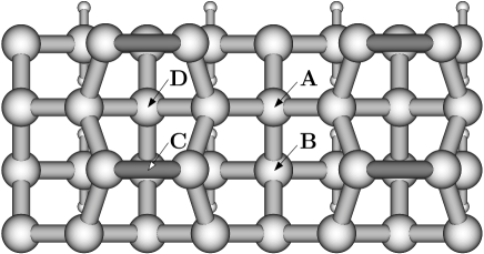
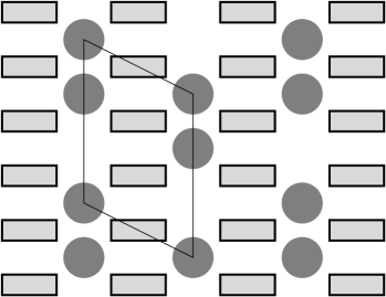
Fig. 1 shows a ball stick model of the silicon surface and introduces the high-symmetry adsorption sites A to D, which we will refer to in the following discussion.
Filling the empty dangling bond with two electrons results in a removal of the buckling as observed in our studies on Sr adsorption.Ashman04 As La has an odd number of valence electrons, we also examined the changes of the buckling upon filling the initially empty dangling bond with a single electron. While the difference in coordinate of the two silicon atoms of a buckled dimer is 0.76 Å and the one of an unbuckled dimer 0.00 Å, it is 0.35 Å after donation of a single electron to a dimer. Thus the amplitude of the dimer buckling may be used as a measure for the electron count.
IV Bulk La silicides
In the case of Sr, the chemical interaction with silicon could be understood by investigating the bulk Sr silicides.Ashman04 All these structures could be explained by the Zintl-Klemm concept.Zintl39 The electropositive Sr atoms donate their two valence electrons to the silicon atoms. Each accepted electron saturates one of silicon’s four valences. A Si- can thus form three covalent bonds, a Si2- only two, a Si3- only one and a Si4- has a closed shell and does not form covalent bonds. This principle was found to also be valid for the surface reconstructions of Sr on Si(001).Ashman04
The Zr silicides on the other hand cannot be explained by the simple Zintl-Klemm concept.Foerst03 The Zr states also contribute to the bonding and thus retain a variable number of electrons.
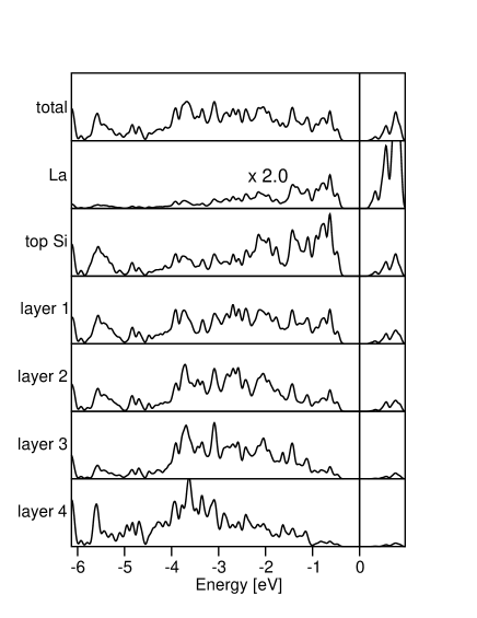
Similarly, the La silicides cannot be simply explained by a quasi-ionic interaction with silicon. We find La in formal charge states between two and three (i.e. charge according to the Zintl-Klemm concept). Also the atom and angular momentum resolved density of states reveals, that La states are partly occupied in these structures.
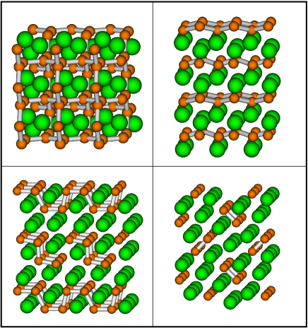
Fig. 2 shows the La silicides. LaSi2 is the lowest energy silicide. The energies per La atom are listed in Table 2.
| E[La] [eV] | |
|---|---|
| LaSi2 | 0.00 |
| LaSi | 0.42 |
| LaSi | 0.62 |
| La3Si2 | 0.80 |
V Ad-atoms and La dimers
Our search for the adsorption structures of La have been guided by the electron count rules that emerged from our investigation of SrAshman04 adsorption on the same surface. The studies of Sr provided a consistent picture: The electrons from Sr are fully transfered into the Si-dimer dangling bonds of the Si substrate. The ordering of Sr atoms on the surface is determined by the electrostatic attraction between the Sr-cations and negatively charged Si-ions at the surface. The negative Si-ions are the raised atoms of buckled Si dimers and the atoms of filled, and thus unbuckled, dimers. This picture holds up to coverages where all Si-dimers are filled at 1/2 ML. Due to the different electron count of La as compared to Sr, we expect that the silicon dimers are filled already at a coverage of 1/3 ML and secondly we anticipate deviations from the above scheme.
Even though we predict La-chains to be the most stable structures in the low coverage limit, we first investigate isolated ad-atomsspin-pol and La-dimers in order to provide an understanding of the constituents of the more extended structures. Chain structures are more stable by 0.34-0.40 eV per La atom as compared to isolated ad-atoms.
Similar to Sr,Ashman04 we find the most stable position of an isolated La atom at position , in the center of four Si-dimers (compare Fig. 1). The position D, B and C have energies 0.23 eV, 0.51 eV and 1.70 eV higher than position . A supercell has been used for these calculations.
The diffusion barrier along the valley is equal to the energy difference between sites and , namely 0.52 eV, the one across the row is 1.31 eV and is estimated by the midpoint between the sites and .
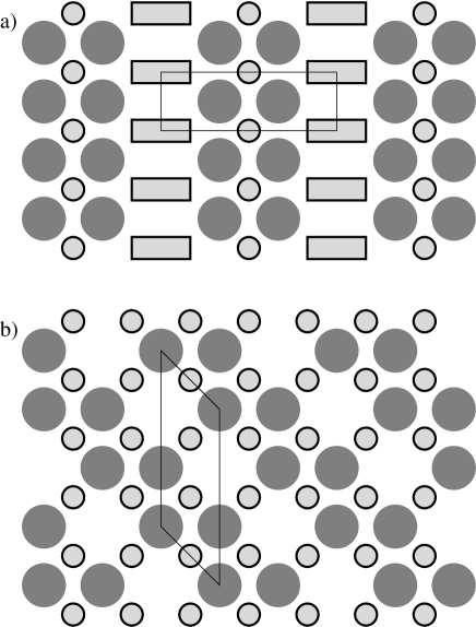
The formation of La dimers lowers the energy per ad-atom by 0.10–0.18 eV compared to isolated ad-atoms. Due to the topology of the Si(001) surface, three different types of La-dimers can be formed: (1) orthogonal to the Si dimer rows, (2) parallel to the Si dimer rows and (3) diagonal to the Si dimer rows. All three structures are shown in Fig. 3. We find that the parallel La-dimer is lowest in energy, followed by the orthogonal and diagonal La-dimers. All La-dimers lie within a small energy window of 0.08 eV. Note, that we only investigated singlet states.
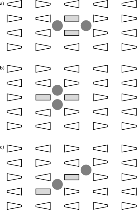
A pair of La atoms has six valence electrons and from the lessons learned from Sr adsorption, one would assume that three Si-dimers in the vicinity of the La-dimer get unbuckled. This is, however, not the case. Only two Si-dimers become fully unbuckled. The remaining two electrons from the La-dimer enter into states that are derived from the upper dangling-bond band and which have an admixture of the La- and states.
Usually one can easily distinguish between buckled and unbuckled dimers. In the vicinity of La-dimers oriented diagonally or orthogonally, however, we also observe Si-dimers with an intermediate buckling amplitude. Thus, in these cases, the oxidation state of the La atom, namely 2+ versus 3+ cannot be attributed in a unique manner.
For the orthogonal and diagonal La-dimers we observe a tendency for the La atoms to reduce their distance compared to staying centered on A sites by 1 – 4 %. For the parallel La-dimer this effect is opposite and much larger. The distance between the two La atoms is 4.11 Å, compared to 3.84 Å between two A sites which amounts to an expansion of 7 %. This ad-atom repulsion within one valley has already been observed in case of SrAshman04 and explains the formation of isolated chains instead of condensed chains or clusters at low coverages. Nevertheless, we find the parallel dimer to be the most stable.
VI Chain structures at low coverages
As we combined pairs of the most favorable site for isolated La ad-atoms into dimers, we now search for ways to stack the three types of La-dimers together into more extended structures.
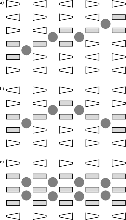
We systematically approached linear chain structures. Each of the three La-dimer types – parallel to the Si-dimer row, orthogonal or diagonal – has been stacked such that it shares at least one Si-dimer, so that this Si-dimer is next to two Lanthanum atoms from different La-dimers. The energetic ordering has been deduced on the basis of binding energy per La atom (compare Tab. 3). Note that the binding energy per La atom for a given chain structure is slightly coverage dependent. In case of the double stepped chains (compare Fig. 4a for the structural principle) the adsorption energy varies within 0.06 eV at coverages between 1/10 and 1/5 ML. In order to ensure comparability all numbers listed here refer to a coverage of 1/6 ML.
We start our investigation with parallel La-dimers shown in Fig. 3b, which is the most stable dimer structure. The most favorable chain in this class is stacked perpendicular to the Si-dimer rows as shown in Fig. 4c. Its energy lies 0.06 eV per La atom above the lowest energy chain structure.
The most favorable chain made from orthogonal La-dimers is shown in Fig. 4a. It can also been interpreted as a variant of a chain of diagonal La-dimers (compare Fig. 3 c). This is the most favorable chain structure of La atoms on Si(001). Its chains run at an angle of about 76∘ to the Si-dimer row. It should be noted that it is equally possible to arrange the La-dimers in a zig-zag manner as shown in 4b. The zig-zag chain has not been explicitly calculated. The coexistence of straight and zig-zag chains has been found for Sr on Si(001), where the two modifications have been shown to be almost degenerate in energy.Ashman04
| La-dimer type | E[La] [eV] | panel | |
|---|---|---|---|
| parallel | 90 | -0.30 | a |
| parallel | 63 | -0.15 | b |
| parallel | 45 | -0.20 | c |
| parallel | 34 | -0.13 | d |
| parallel | 0 | -0.07 | e |
| orthogonal | 90 | -0.26 | f |
| orthogonal/diagonal | 76 | -0.36 | g |
| diagonal | 63 | -0.28 | h |
In all low-energy structures each La atom is thus surrounded by four silicon atoms having filled dangling bonds. Three of them are partners of filled Si-dimers while one is a buckled Si-dimer with the negative Si atom pointing towards the La ad-atom. On the basis of counting unbuckled Si-dimers, these structures are in a 3+ oxidation state.
The La-chain is the configuration with lowest energy in the low coverage limit. The lowest energy chain structures are of the order of 0.17 eV per La atom more stable than the most favorable isolated La-dimer. At elevated temperatures, entropic effects will lead to increasingly shorter chain fragments. From the energy-difference of the linear chain and the isolated La-dimer, we obtain an estimate for the chain termination energy of approximately 0.09 eV. It should be noted, that experiments often observe shorter chain sequences than predicted from thermal equilibrium as high-temperature structures are frozen in.
The electronic structure of the La-chain is analogous to that of the Sr single chain.Ashman04 The empty silicon surface has an occupied and an un-occupied band formed from the dangling bonds of the Si-dimers. La donates electrons into the upper dangling bond band. Those dangling bond states, which become filled, are shifted down in energy due to the change in hybridization on the one side and due to the proximity of the positive La-cations on the other side.
VII Condensed chains
With increasing coverage, the chains become closer packed. In the case of Sr, there was a preference for a periodicity of surface lattice spacings along the Si-dimer row direction.Ashman04 This restriction has been attributed to the requirement that every cation be surrounded by four Si-atoms with filled dangling bonds, and that there is no frustration of the Si-dimer buckling, i.e. adjacent Si-dimers are buckled antiparallel.
For La the situation is more complex. Due to the longer periodicity of the La chains compared to those of Sr, there are two families of chain packing for La as shown in Fig. 6. In the first family the La chains are displaced only parallel to the Si-dimer row direction. In the second family the chains are in addition displaced perpendicular to the Si-dimer row.
The first family has a preference of surface lattice spacings along the dimer row as in the case of Sr adsorption. The spacing in the second family is arbitrary. The reason is that in family one, the buckling of every second Si-dimer row is pinned on both sides by two neighboring La chains (see Fig. 6a). A Si-dimer is pinned, if its buckling is determined by the Coulomb attraction of its raised, and thus negatively charged, Si atom to a nearby La ion. Since the buckling alternates along the Si-dimer row, this pinning can lead to indirect, long-ranged interaction between different La-chains.
In the second family the buckling of every Si-dimer row is pinned only at one La-chain as seen in Fig. 6b, while there is no preference of the Si-dimer buckling at the other La-chain. Thus for La we find – in contrast to SrAshman04 – arbitrary chain spacings.

The closest packing of La-chains before they merge is 1/5 ML. We consider two La-chains merged if La atoms of different La chains occupy nearest-neighbor sites within one valley. We predict a distinct phase at this coverage as seen in Fig. 12 and discussed later. This structure, shown in Fig. 6b, is derived from chains of the second family. An explanation for finding a phase at 1/5 ML is that the energy at higher coverage increases due to the electrostatic interaction of the La atoms within one valley. For the first family, the highest possible coverage before La-chains merge is 1/6 ML (Fig. 6a).
Note that the chains can change their direction without appreciable energy cost as shown in Fig. 4b. Experimentally measured diffraction patterns would reflect a configurational average.
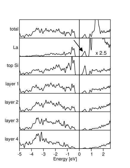
The layer resolved density of states is shown in Fig. 5. We see that the Fermi-level lies in a band gap of the surface. Above the Fermi-level and still in the band-gap of bulk Si, surface bands are formed, which originate from the remaining empty dangling bonds of the buckled Si-dimers. As in the case of Sr, these states form flat bands in the band-gap of silicon, which approximately remain at their energetic position as the La coverage is increased. Its density of states, however, scales with the number of empty dangling bonds.
VIII The canonical surface at 1/3 ML coverage
If the spacing of the chains is further reduced, they condense at 1/3 ML to the structure shown in Fig. 7.
There are several versions of this structure type. They have a repeating sequence of two La-atoms and one vacant site in each valley in common. The relative displacement of this sequence from one valley to the next, however, may differ. We investigated several structures and found the one shown in Fig. 7 to be the most stable.
A structure with a sequence of four sites occupied with metal ions separated by two empty sites, has been the most favorable structure at this coverage in the case of Sr adsorption.Ashman04 For La, however, this configuration is energetically unfavorable.
At a coverage of 1/3 ML, all silicon dangling bonds are filled due to the electrons provided by the La ad-atoms. This surface is isoelectronic to the Sr covered surface at 1/2 ML.Ashman04 For the Sr-covered silicon surface, the increased oxidation resistance of the corresponding 1/2 ML structure has been observed experimentally.Liang01 Similarly we suggest that the surface covered with 1/3 ML of La will have an increased oxidation resistance.
In Fig. 8 we show the layer-resolved density of states of the most stable structure at 1/3 ML. In analogy to the 1/2 ML covered Sr surface, there are no surface states deep in the band gap of silicon, because all Si-dimer dangling bonds are filled and shifted into the valence band due to the electrostatic attraction of the electrons to the positive La ions. Note, however, that in contrast to the canonical surface coverage of Sr on Si(001) at a coverage of 1/2 ML, the canonical La surface exhibits vacant -sites.
IX Transition from La3+ to La2+ above 1/3 ML
Up to the canonical coverage of 1/3 ML, all thermodynamically stable reconstructions could be explained by La being in the oxidation state. In contrast to the isolated La-atoms and La-dimers, the oxidation state can clearly be identified from the number of unbuckled Si-dimers: Each unbuckled dimer has received two electrons. A oxidation state is also consistent with the density of states.
If we follow the picture that emerged from Sr, we would anticipate that increasing the coverage above 1/3 ML in case of La would lead to filling the Si-dimer antibonds, which results in a breaking up of the dimer bonds. For La the situation is different: the La- band is located at much lower energies as compared to Sr. Therefore the energy to break the Si-dimer bonds is larger than that to add electrons into the La -shell. As a result we find that La changes its oxidation state from to . Oxidation states of La that are even lower are unfavorable due to the Coulomb repulsion of electrons within the La- and shells. Thus the structures above 1/3 ML can be explained in terms of La2+ ions and are similar to those found for Sr.Ashman04
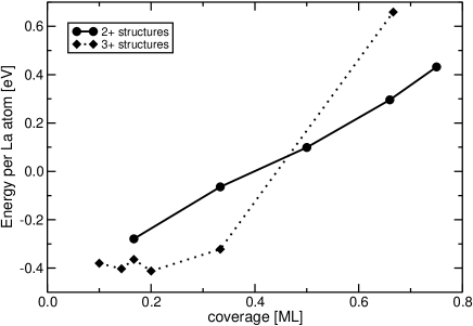
It may be instructive to compare two structures with different oxidation states of La. A good example is found at a coverage of 2/3 ML: The lowest energy structure is a reconstruction already found for SrAshman04 and depicted in Fig. 9a. This is a clear 2+ structure. Since every Si-dimer only accepts two electrons, they can just accommodate two of the three valence electrons of La. The lowest structure with formal La3+ ions, which can clearly be identified as having all Si-dimer bonds broken, is shown in Fig. 9b. It has an energy which is 0.36 eV per La atom higher than the structure with La2+ ions.
At 1/2 ML, we find a structure where all sites are occupied to be most stable. There the La -states are partially occupied. We confirmed that the system is not spin polarized.
The crossover of the energy surfaces of the 2+ and the 3+ structures is shown in Fig. 10 using a set of surface reconstructions, for which the charge state can be determined unambiguously. It can be clearly seen that the 2+ structures become significantly more stable above 1/2 ML. From Fig. 11 it is apparent that the energy rises sharply as the La atoms cross over to the 2+ oxidation state beyond the canonical interface at a coverage of 1/3 ML.
X Phase diagram
Based on the surface energies composed in Fig. 11 we extracted the zero-Kelvin phase diagram shown in Fig. 12. The slope of the line-segments of the lower envelope in Fig. 11 corresponds to the chemical potential, at which the two neighboring phases coexist (for a more elaborate discussion, refer to Ref.Ashman04 ). The stable phases are defined by the coverages where two line segments with different slopes meet. The zero for the La chemical potential has been chosen as the value at which LaSi2 and silicon coexist. Consequently, all phases in regions of positive chemical potentials are in a regime where the formation of bulk silicides is thermodynamically favorable.
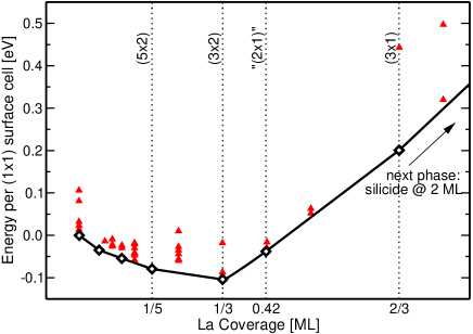
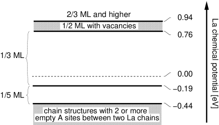
Below a chemical potential of eV we expect single chain structures as described in Sec. VI. At 1/5 ML we predict a distinct phase since this is the highest possible coverage without La ad-atoms at nearest neighbor sites (compare Fig. 6b). At a chemical potential of -0.19 eV the stability region of the 1/3 ML coverage (Fig. 7) starts.
The transition from the phase at 1/3 ML to the reconstructed surface at 1/2 ML, where all -sites are filled, can be described by a decrease of La-vacancies (compare Fig. 7 of this manuscript and Fig. 9 of Ref. Ashman04 ). From this point of view, the phase at 1/3 ML can be described by an ordered array of La-vacancies in the 1/2 ML structure. There is an effective repulsion between La-vacancies due to the repulsion between La-atoms on neighboring -sites. We describe the total energy by an empirical model energy of the form , where is the concentration of La vacancies, is the energy of the structure with all -sites filled (1/2 ML), is the formation energy of an isolated La-vacancy, and describes the repulsion between vacancies. Coexistence between the two phases would result from a negative value of . In that case, adding an additional ad-atom to a phase requires more energy than starting a new phase with the next higher coverage. Between 1/3 and 1/2 ML, however, is positive as filling a portion of vacancies is favorable compared to creating patches of pure 1/2 ML coverage.
We calculated the energy of an adsorption structure with three La atoms on neighboring sites separated by one vacancy within one valley. La triplets in different valleys have been arranged, so that the distance between vacancies is maximized in order to minimize the repulsive energy. Based on the energies at 1/3 and 1/2 ML as well as at the intermediate coverage of 3/8 ML just described, we can determine the three parameters , and to be 0.05, -0.56 and 0.26 eV, respectively.
At a certain vacancy concentration of % (i.e. a La-coverage of 0.42 ML) we find a phase boundary with the next stable phase at 2/3 ML at a chemical potential of 0.94 eV. According to our phase diagram, the pure surface reconstruction at 1/2 ML is never formed. The shaded region in Fig. 12 corresponds to 1/2 ML structural template with variable vacancy concentration.
As seen in the phase diagram shown in Fig. 12 bulk silicide formation becomes thermodynamically stable within the stability region of the 1/3 ML coverage. In a growth experiment we would expect the formation of bulk silicide grains to be delayed beyond a coverage of 1/3 ML. The nucleation of silicide grains may suffer from the large mismatch between bulk silicide phases and silicon. This is of particular importance during the initial stages of nucleation because the strained interface region occupies most of the volume of the grain.
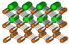
Thus it may be of interest to know the stability of silicide thin films on Si(001). We found one such silicide layer which is shown in Fig. 13. It consists of a silicon surface in contact with two La layers that sandwich a layer of Si4- ions in between. While we have not performed a thorough search of other candidates, the energy of this silicide layer indicates that silicide formation will at the latest be initiated beyond a coverage of 2/3 ML. We can thus only pin down the onset of silicide formation within a coverage interval between 1/3 (thermodynamically) and 2/3 ML (including kinetic considerations).
XI Conclusions
In this paper we have investigated the surface structures of La adsorbed on Si(001) as a function of coverage. We propose a theoretical phase diagram by relating the phase boundaries at zero temperature to chemical potentials, which can be converted into partial pressure and temperature in thermal equilibrium.
Our findings elucidate the chemistry of third row elements on Si(001) and the phases of La on Si(001), and are expected to provide critical information for the growth of a wide class of high-k oxides containing La. The phase diagram may be used as a guide for the growth of La-based oxides on Si(001).


Appendix A Supercells at dilute coverages
Fig. 3 shows the three possible La-dimer orientations on the Si(001) surface. We did not draw the periodic images introduced by the calculational supercell in order to emphasize that fact that this local arrangement corresponds to an isolated dimer. Fig. 14 sketches the supercells used. They were chosen in order to avoid frustration of Si dimers due to periodic images.
Acknowledgements.
We thank A. Dimoulas, J. Fompeyrine, J.-P. Loquet, G. Norga and C. Wiemer for useful discussions. This work has been funded by the European Commission in the project ”INVEST” (Integration of Very High-K Dielectrics with CMOS Technology) and by the AURORA project of the Austrian Science Fond. Parts of the calculations have been performed on the Computers of the “Norddeutscher Verbund für Hoch- und Höchstleistungsrechnen (HLRN)”. This work has benefited from the collaborations within the ESF Programme on ’Electronic Structure Calculations for Elucidating the Complex Atomistic Behavior of Solids and Surfaces’.References
- (1) Corresponding author: peter.bloechl@tu-clausthal.de
- (2) G.E. Moore, SPIE 2438, 2 (1995)
- (3) International Technology Roadmap for Semiconductors, 2001 Ed. http://public.itrs.net/
- (4) R.A. McKee, F.J. Walker and M.F. Chisholm, Phys. Rev. Lett. 81, 3014 (1998).
- (5) M. V. Cabañas, C. V. Ragel, F. Conde, J. M. González-Calbet, M. Vallet-Regí, Solid State Ionics, 101, 191, (1997).
- (6) M. Nieminen, T. Sajavaara, E. Rauhala, M. Putkonen and L. Niinistö, J. Mater. Chem., 11, 2340, (2001).
- (7) B.-E. Park and H. Ishiwara, Appl. Phys. Lett., 79, 806, (2001).
- (8) G.D. Wilk, R.M. Wallace and J.M. Anthony, J. Appl. Phys. 89, 5243 2001.
- (9) S. Guha, N.A. Bojarczuk, and V. Narayanan, Appl. Phys. Lett. 80, 766 (2002)
- (10) S. Guha, E. Cartier, M.A. Gribelyuk, N.A. Bojarczuk, and M.C. Copel, Appl. Phys. Lett. 77, 2710 (2000)
- (11) G. Apostolopoulos, G. Vellianitis, A. Dimoulas, J.C. Hooker and T. Conard App. Phys. Lett., 84, 260 (2004).
- (12) J. Fompeyrine, G. Norga, A. Guiller, C. Marchiori, J. W. Seo, J.-P. Locquet, H. Siegwart, D. Halley, C. Rossel in Proceedings of the WODIM 2002, 12th Workshop on Dielectrics in Microelectronics (IMEP, Grenoble, France, 2002), p. 65.
- (13) J. W. Seo, J. Fompeyrine, A. Guiller, G. Norga, C. Marchiori, H. Siegwart, and J.-P. Locquet, App. Phys. Lett, 83, 5211, (2003).
- (14) H.J. Osten, J.P. Liu, H.-J. Müssig and P. Zaumseil, Microelectronics Reliability 41, 991 (2001)
- (15) C.J. Först, K. Schwarz and P.E. Blöchl, Comp. Mater. Sci. 27, 70 (2003).
- (16) C.R. Ashman, C.J. Först, K. Schwarz and P.E. Blöchl, Phys. Rev. B 69, 75309 (2004).
- (17) Y.M. Sun, J. Lozano, H. Ho, H.J. Park, S. Veldmann and J.M. White, Appl. Surf. Sci. 161, 115 (2000)
- (18) C.J. Först, C.R. Ashman, K. Schwarz and P.E. Blöchl, Nature 427, 53 (2004).
- (19) G.J. Norga, A. Guiller, C. Marchiori, J.P. Locquet, H. Siegwart, D. Halley, C. Rossel, D. Caimi, J.W. Seo, and J. Fompeyrine, Materials Research Society Symp. Proc. 786, E 7.3.1 (2004).
- (20) P. Hohenberg and W. Kohn, Phys. Rev. 136, B864 (1964).
- (21) W. Kohn and L.J. Sham, Phys. Rev. 140, A1133 (1965).
- (22) J.P. Perdew, K. Burke, and M. Ernzerhof, Phys. Rev. Lett. 77, 3865 (1996).
- (23) P.E. Blöchl, Phys. Rev. B 50, 17953 (1994).
- (24) Peter E. Blöchl, Clemens J. Först and Johannes Schimpl, Bull. Mater. Sci. 26, 33 (2003)
- (25) R. C. Weast, CRC Handbook of Chemistry and Physics, 83rd ed., CRC Press, Inc., Boca Raton, 2002, p. 4-164.
- (26) R. Car and M. Parrinello, Phys. Rev. Lett. 55, 2471 (1985).
- (27) N. D. Mermin, Phys. Rev. 137, A1441 (1965).
- (28) M. Gillan, J. Phys: Cond. Mat. 1, 689 (1989)
- (29) E. Zintl, Angew. Chem. 52, 1 (1939); W. Klemm, Proc. Chem. Soc. London 1958, 329; E. Bussmann, Z. Anorg. Allg. Chem. 313, 90 (1961).
- (30) H. Nakano, S. Yamanaka, J. Sol. Stat. Chem. 108, 260-266, (1994).
- (31) D. Hohnke, E. Parthe, Act. Cryst. A 20, 572-582, (1966)
- (32) H. Mattausch, O. Oeckler, A. Simon, Z. Anorgan. Alg. Chemie A 625, 1151-1154, (1999).
- (33) E. I. Gladyshevskii, IVNAM 1, 648-651, (1965).
- (34) The isolated La atom has one unpaired electron. Hence the calculations have been performed spin polarized. Due to the periodic boundary conditions, the unpaired electron enters a delocalized, partially filled band. As a result most of the calculations on isolated defects produced no net spin.
- (35) Y. Liang, S. Gan, and M. Engelhard, App. Phys. Lett., 79, 3591 (2001).
- (36) The adsorption energy per unit cell is defined as , where is the total energy of the supercell used for the specific surface reconstruction, is the number of surface unit cells contained in that supercell and is the slab-thickness in units of silicon layers of the supercell. denotes the number of La atoms in the supercell and the La coverage for that reconstruction. This energy can be alternatively calculated using the energy per La atom multiplied with the coverage . The reference energies are listed in Tab. 1.