The antiferromagnetic transition of UPd2Al3 break-junctions: A new realization of -shaped current-voltage characteristics
Abstract
We have investigated metallic break junctions of the heavy-fermion compound UPd2Al3 at low temperatures between 0.1 K and 9 K and in magnetic fields up to 8 T. Both the current-voltage characteristics and the d/d spectra clearly showed the superconducting ( K) as well as the antiferromagnetic (14 K) transition at low temperatures when the bias voltage is raised. The junctions with lateral size of order 200 nm had huge critical current densities around A/m2 at the antiferromagnetic transition and hysteretic characteristics. Degrading the quality of the contacts by in situ increasing the local residual resistivity reduced the hysteresis. We show that those hysteretic curves can be reproduced theoretically by assuming the constriction to be in the thermal regime. It turns out that these point contacts represent non-linear devices with -shaped characteristics that have a negative differential resistance like an Esaki tunnel diode.
pacs:
73.63.-b, 74.25.Fy, 74.50.+r1 Introduction
Point-contact (PC) spectroscopy is widely used to study the interaction of conduction electrons with elementary excitations or quasiparticles in conducting solids [1, 2]. Energy-resolved PC spectroscopy is possible when the inelastic relaxation length of electrons in the contact region (here and are the elastic and the inelastic mean free path of the electrons) is larger than the size or diameter of the contact. In the opposite case of and a short phonon scattering length , the excess electron energy dissipates in the constriction. This Joule heating increases the temperature inside the contact when a bias voltage is applied [3, 4, 5].
Therefore the interpretation of the PC data requires to find out the regime of charge transport. does not depend on energy and can be determined rather accurately for the PC region. depends on energy, and no method exists to calculate it reliably. To identify the transport regime becomes especially important for PCs with complex systems like heavy-fermion, high-Tc, or Kondo-lattice compounds that typically have large electrical resistivities because of their strong electron correlations.
A. Wexler [6] derived
| (1) |
for the PC resistance as function of temperature and contact size . The parameter varies slowly as function of , and for large contacts . Wexler’s formula interpolates between the ballistic Sharvin () and the diffusive Maxwell () resistance. The latter describes transport as in the bulk material.
Since Sharvin’s resistance does not depend on temperature, differentiating Eq. (1) with respect to temperature yields
| (2) |
for the size of the contact. This is considerably more reliable for deriving than Eq. (1) itself. The main reason is that the residual resistivity in the PC region can strongly differ from the bulk , for example due to the stress exerted while forming the contact. Eq. (2) was experimentally verified for PCs with simple metals by Akimenko et al[7].
The same method can be applied to heavy-fermion compounds. They show at low temperatures power-law dependencies of their electrical resistivities ( for the various compounds investigated) which was also revealed in the PC resistances [8]. Heavy-fermion compounds typically have large coefficients because of their strong electron correlations, which makes it straightforward to measure just above . For those high-resistivity superconducting (SC) metals the local normal-state residual resistivity in the PC region
| (3) |
can be extracted from the drop of the contact resistance due to SC. Such a relationship has been found for a number of heavy-fermion SCs over a wide range of contact sizes [9, 10, 11].
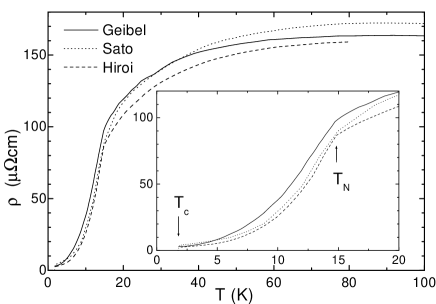
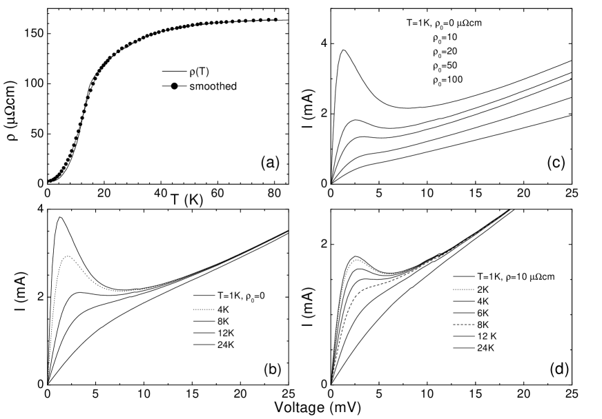
Here we present experiments on PCs between two pieces of the heavy-fermion compound UPd2Al3 [12], using the technique of mechanically-controllable break junctions. Compared to the conventional spear-anvil type technique to form point contacts, break junctions have much better mechanical stability. But more importantly breaking the sample at low temperatures in the ultra-high vacuum region of the refrigerator avoids oxidation of the freshly broken surfaces of the contact interface. UPd2Al3 becomes antiferromagnetic (AFM) at 14 K. It is SC below K. We have observed huge non-linearities of the PC resistances and even hysteretic characteristics. We derived the contact size and the residual resistivity in the PC region according to Eqs. (2) and (3), respectively. We found that the very short elastic mean-free path in the constriction points to at least the diffusive regime of electron transport through the PC. Considering also the small inelastic mean-free path in UPd2Al3, reflected by the steep rise with temperature around the AFM transition in Fig. 1, we applied the thermal model developed in Refs. [4, 5] for the case to take into account the locally increased temperature in the PC when a bias voltage is applied. Using the experimental in Fig. 1, this model described quite well the observed characteristics and their modification with temperature, reproducing also the hysteretic features.
2 Experiment
We have investigated three UPd2Al3 single crystals. Two of them had one long side in the c-direction of the hexagonal crystal lattice, one sample had it in the perpendicular ab-direction. A mm deep notch was cut into the middle of the mm3 large UPd2Al3 bars using a diamond saw. This defined the break position. Each sample was glued electrically isolated onto a flexible metal bending beam. Twisted pairs of voltage and current leads were attached with silver epoxy to both sides of the sample, which was then mounted onto the mixing chamber inside the vacuum can of the dilution refrigerator. The temperature could be varied between 0.1 and 9 K. With a micrometer screw the bending beam is bent at low temperatures, breaking the sample at the notch. The resistance of the break junction, that is its lateral contact size, could be adjusted mechanically with the micrometer screw. For further details of the experimental setup see Refs. [10, 11].
At room temperature the resistance of the samples with the notch was about 5 m, corresponding to the approximate geometrical cross-section and a contact size of 0.2 mm. Note that the notch only defines the macroscopic position of the junction, the microscopic contact is less well defined. After removing the sample from the refrigerator, the surface of the junction was not mirror-like or smooth as expected for a single crystal. The fracture was usually tilted with respect to the direction of the notch, and thus the crystal axis. Therefore the current flow through the contact might deviate slightly from the direction defined by the long side of the sample. Magnetic fields up to 8 T could be applied perpendicular to the bending mean, that is perpendicular to the long side of the samples and to the ideal direction of current flow.
The characteristic and the differential resistance were recorded by injecting a DC current superposed by a small alternating current and measuring the differential voltage drop . Its alternating part was detected using the standard lock-in technique.
3 Results
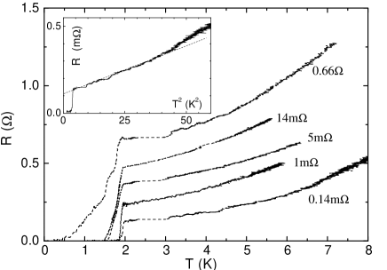
All three UPd2Al3 single crystals showed qualitatively the same results. Therefore we concentrate here on one of them, that with the long side in ab-direction. Figure 2 shows the temperature dependence of the resistance of the break junctions below 9 K before breaking and of several contacts after successively reducing the contact size by increasing the bending force. The superconducting transition at 1.8 K as well as the increase above like in the bulk samples is clearly seen. Occasionally changes in small steps. The reason for this is that UPd2Al3 single crystals are quite brittle. They also have a large thermal expansion with respect to the bending beam above K. When the temperature changes, the stress in the contact region changes. This stress is sometimes partly released, slightly varying the contact size or the local residual resistivity and, thus, .
With increasing PC resistance the SC transition broadens. We believe that this is mainly due to the stress in the PC area when the sample is broken and the contact being formed. Additional broadening is caused by the extremely small critical supercurrent which suppresses the Sharvin resistance at low temperatures and small excitation voltages, see also the discussion below. On increasing the temperature the critical current decreases, so that Sharvin’s resistance is again added to the total resistance. However, its contribution to is small since for the investigated contacts Sharvin’s resistance is much smaller than Maxwell’s resistance. Changing the force on the bending beam changes the contact size and the stress there, too. This allows us, although in an uncontrolled manner, to vary in situ the local resistivity at the PC.

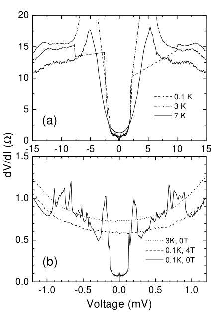
Figure 3 shows for the UPd2Al3 break junction with as example how the curves typically change with temperature. At low temperatures is strongly hysteretic. At higher temperatures the hysteresis smears out and transforms into an inflection point that corresponds to the pronounced maxima above about 5 K in Fig. 4(a). Large magnetic fields up to T only slightly modified the curves at 0.1 K by reducing the size of the hysteretic loop. A 4 T field as well as the temperature above completely suppressed the superconducting features, a zero-bias minimum of the differential resistance accompanied by a series of spikes, see Fig. 4(b).
4 Discussion
We start the analysis by deriving the size of the contacts. Above both the specific resistivity and the contact resistance vary with the same power law. According to Eq. (2) the contact size . Literature values for the coefficient range from 0.15 to cm K-2, for example in Refs. [12, 14, 15]. In part this variation could be due to micro-cracks in the bulk samples which spoils the geometrical factor. Therefore we choose the average cm K-2, which coincides with that in [14]. The absolute error in can then amount up to about , but the relative accuracy needed to compare the different contacts is much better. In this way the contact in Fig. 3 has nm.
We can now directly read off the critical current density from the data in Fig. 3. For the AFM transition the current density reaches up to Am-2. At the SC transition, marked by the maximum in Fig. 4(b), the critical current density approaches Am-2. Both values are lower bounds for the kinetic critical current densities because they include local heating of the PC discussed below.
According to Eq. (3) the resistance drop due to SC results then in a normal-state residual resistivity cm. This is about three times larger than the bulk , estimated from of the unbroken junction in Fig. 2.
This includes a possible contribution from the Josephson effect: The differential resistance vanishes completely within a very narrow (V) voltage range around zero bias, barely seen in Fig. 4. The much broader (mV) zero-bias minimum has a plateau of around , fitting well the ballistic Sharvin resistance calculated using the known contact diameter. This agreement supports our interpretation that we are dealing not with multiply connected contacts but with single contacts. Taking into account Sharvin’s resistance would slightly reduce the calculated local residual resistivity from cm to cm.
The elastic electron mean free path at low temperatures can be estimated using the typical metallic m2 (here is the elastic mean free path and and values taken from [12]) as nm. This leads to the inequality nmnm for two of the important length scales of the constriction, implying that these PCs are at least in the diffusive regime. However, heavy-fermion compounds typically have a large residual resistivity and/or already at low temperatures a strongly increasing electrical resistivity, they are very likely in the thermal regime [16].
The ballistic Sharvin resistance is then negligible, and the PC resistance can be described by Maxwell’s resistance
| (4) |
In contrast to a ballistic contact, where energy dissipates far away form the contact region, now all energy is released in the constriction. This increases its temperature with bias voltage. Assuming the Wiedemann-Franz law to be valid, the temperature in the center of the PC depends on the applied voltage via [3, 4]
| (5) |
When the temperature of the bulk sample vanishes, the contact temperature varies linearly with bias voltage like . Using the standard Lorenz number V2K-2, a 1 mV bias voltage will raise the temperature of the contact by 3.2 K.
In the thermal regime the characteristic of the contact depends on the temperature-dependent electrical resistivity according to [4, 5]
| (6) |
where is defined by Eq. (5). We used the smooth curve in Fig. 5(a) to approximate the experimental , but omitted the SC transition.
The calculated curves in Fig. 5(b) had maxima at around mV, which results in a hysteresis for up- and downward sweeps when the junction is driven by a current source. These maxima are the larger the steeper the drop in around . They decrease and become broader with increasing residual resistivity, see Fig. 5(c).
With voltage biasing we would expect to recover the full chracteristics without hysteresis. However, this would require to install small resistors near the sample in parallel and in series with the break junction to cut off its bistability, see for example Ref. [17]. This was not practical in our experiments because in each cool down we wanted to investigate many break junctions over a wide range of resistances.
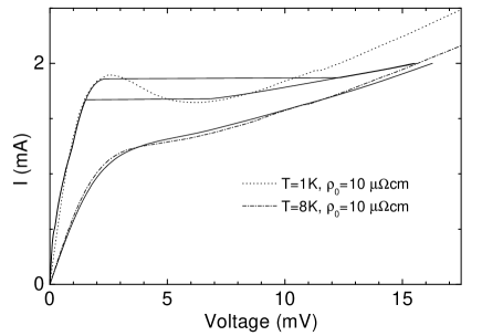
Figure 6 shows that the theoretical describe well the experimental data, including the width of the hysteretic features, using nm and cm. These are the only two adjustable parameters. And they fit well those parameters that have been derived above independently from the measured . This agreement strongly supports our interpretation that local (at the PC) thermal effects determine the behavior of our UPd2Al3 break junctions.
Surprisingly, the standard Lorenz number yields the best fit to the experimental curves while in bulk UPd2Al3 rises from 0.6 below 1 K up to at 24 K because of the dominant heat transport by phonons [15]. This implies that at the PC the phonon channel is closed, and heat is carried away by electrons only.
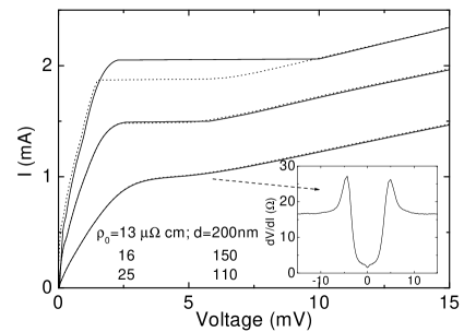
With increasing residual resistivity the hysteresis of the experimental curves in Fig. 7 transforms into an inflection point, corresponding to the maxima in (inset of Fig. 7). This trend agrees with the theoretical curves in Fig. 5(c). However, it seems that with increasing the experimentally observed hysteresis disappears more quickly than expected from theory. One could speculate that the larger the more strongly degraded is the contact structure, simultaneously broadening the steep rise of around the AFM transition, see inset in Fig. 1 in Ref. [18]. Such a broadening would be similar to that of the SC transition of the PC in Fig. 2.
The slightly reduced size of the hysteresis loops in an applied magnetic field, shown in the lower inset of Fig. 3, goes in the same direction. This could be attributed to a small positive magnetoresistivity of UPd2Al3 [19].
Note that the AFM transition itself is difficult to resolve in the characteristics. This transition shows up as a small step in the derivative of . Since is described by an integral containing over a certain range of temperatures defined by the bias voltage, one would at least have to check the second derivative . Nevertheless, the huge anomalies in reflect the AFM transition because the magnetic ordering improves dramatically the coherence of the electron scattering processes, leading to the steeply decreasing resistivity.
In the characteristics SC appears as an ’excess’ current, see the upper inset of Fig. 3. To calculate of the superconducting anomaly we assumed that varies like the contact resistance (see Fig. 2), normalized to the normal-state . This lead to a single peak at around 0.15 mV, while the experimental in the upper inset of Fig. 3 rises almost continuously. Thus the thermal model [4, 5], developed for normal-state contacts, fails to describe even qualitatively the resistance of the SC contacts. This failure could have two reasons. First, the broad SC transition indicates that the contact does not have a single , but a whole distribution ranging from at the center of the contact where it is reduced due to stress and disorder and K far away in the indisturbed bulk material.
A multiply connected contact, where each connection has its own creating a single spike in the spectrum, could be excluded because Sharvin’s resistance was recovered. Consequently also the normal-state residual resistivity may vary locally, both along and vertical to the contact direction, while Eqs. (5) and (6) have been derived for homogeneous samples only. This would greatly affect the characteristic at low bias voltages since the pattern of current flow could change abruptly, for example when the critical supercurrent is exceeded in part of the contact region. It will not change at large bias voltages because then the large -dependent part of the electrical resistivity takes over. Second, at low temperatures, when both the elastic and the ineleastic electron mean free paths are largest, the UPd2Al3 contacts could be in the diffusive instead of the thermal regime. With increasing temperature or bias voltage the mean free paths get smaller, and the contact is forced into the thermal regime again.
Break junctions with URu2Si2, another heavy-fermion SC, had peaks in the differential resistance at voltages described by Eq. (5) [10]. This indicated the destruction of SC in the constriction due to local heating. We have observed the same behavior also for our UPd2Al3 contacts in the SC state.
The UPd2Al3 junctions presented here are non-linear devices. Their -shaped characteristics have a negative differential resistance. Those devices could be applied – in principle – like an Esaki tunnel diode or a Gunn diode as amplifiers, generators, or switching units [20, 21]. Of practical interest is therefore the possible minimum response time. We estimate it by the thermal relaxation time of the contact [4]. Here is the thermal heat capacity per volume, is material density and the thermal conductivity. With the molar heat capacity of J/K-1mol-1 [12], g cm-3, and W K-1m-1 [15] at 10 K the relaxation time becomes ps for a nm wide contact. This is three orders of magnitude larger than for a standard tunnel diode, but it could be reduced by using smaller contacts as long as they remain in the thermal regime. One (dis)advantage, however, is the low mV working point (at the maximum negative slope of ), an order of magnitude below that of typical Esaki tunnel diodes.
5 Conclusion
Sub-m scale metallic break-junctions of heavy-fermion UPd2Al3 showed hysteretic characteristics at low temperatures. These highly nonlinear curves can be reproduced theoretically by assuming the constrictions are in the thermal regime. Such anomalous curves are due to the unusual dependence of UPd2Al3 at the AFM transition. Since those point contacts with -shaped characteristics are nonlinear elements with a negative differential resistance, they could serve as the analogue of Esaki tunnel diodes or Gunn diodes as amplifiers, generators, and switching units. From this point of view UPd2Al3 is not such a unique material – each metal with similar should produce similar characteristics. This can be expected for many materials which order magnetically at low temperatures, since their resistivity typically increases steeply when magnetic order is destroyed by thermal fluctuations.
References
- [1] I. K. Yanson, Sov. J. Low Temp. Phys. 9, 343 (1983); I. K. Yanson and O. I. Shklyarevskii, Sov. J. Low Temp. Phys. 12, 509 (1986).
- [2] A. Duif, A. G. M. Jansen, and P. Wyder, J. Phys.: Condens. Matter 1 , 3157 (1989).
- [3] N. Kohlrausch, Ann. Physik (Leipzig) 1, 132 (1900).
- [4] B. I. Verkin, I. K. Yanson, I. O. Kulik, O. I. Shklyarevskii, A. A. Lysykh, and Yu. G. Naidyuk, Solid State Commun. 30, 215 (1979); Izv. Akad. Nauk SSSR, Ser. Fiz. 44, 1330 (1980).
- [5] I. O. Kulik, Sov. J. Low Temp. Phys. 18, 302 (1992).
- [6] A. Wexler, Proc. Phys. Soc. (London) 89, 927 (1966).
- [7] A. I. Akimenko, A. B. Verkin, N. M. Ponomarenko, and I. K. Yanson, Sov. J. Low Temp. Phys. 8, 130 (1982) [Fiz. Nizk. Temp. 8, 260 (1982)].
- [8] K. Gloos, F. B. Anders, B. Buschinger, C. Geibel, K. Heuser, F. Jährling, J. S. Kim, R. Klemens, R. Müller-Reisener, C. Schank, and G. R. Stewart, J. Low Temp. Phys. 105, 37 (1996).
- [9] K. Gloos, F. B. Anders, B. Buschinger, and C. Geibel, Physica B 230-232, 391 (1997).
- [10] Yu. G. Naidyuk, Gloos K. and Menovsky A. A., J. Phys.:Cond. Matter 9, 6279 (1997).
- [11] K. Gloos, F. B. Anders, W. Assmus, B. Buschinger, C. Geibel, J. S. Kim, A. A. Menovsky, R. Müller-Reisener, S. Nuettgens, C. Schank, G. R. Stewart, and Yu. G. Naidyuk, J. Low Temp. Phys. 110, 873 (1998).
- [12] C. Geibel, C. Schank, S. Thies, H. Kitazawa, C. D. Bredl, A. Böhm, M. Rau, A. Grauel, R. Caspary, R. Helfrich, U. Ahlheim, G. Weber, and F. Steglich, Z. Phys. B 84, 1 (1991).
- [13] N. Sato, T. Sakon, N. Takeda, T. Komatsubara, C. Geibel, F.Steglich, J. Phys. Soc. Jpn. 61 32 (1992).
- [14] N. Sato, Y. Inada, T. Sakon, K. Imamura, A. Ishiguro, J. Kimura, A. Sawada, T. Komatsubara, H. Matsui, T. Goto, IEEE Transactions on Magnetics, 30 1145 (1994).
- [15] M. Hiroi, M. Sera, N. Kobayashi, Y. Haga, E. Yamamoto, and Y. Onuki, J. Phys. Soc. Japan 66, 1595 (1997).
- [16] Yu. G. Naidyuk, and I. K. Yanson, J. Phys.: Condens. Matter 10 , 8905 (1998).
- [17] M. L. Leadbeater, E. S. Alves, M. Henini, O. H. Hughes, A. Celeste, J. C. Portal, G. Hill, and M. A. Pate, Phys. Rev. B 39, 3438 (1989).
- [18] O. E. Kvitnitskaya, Yu. G. Naidyuk, A. Nowack, K. Gloos, C. Geibel, A. G. M. Jansen, and P. Wyder, Physica B 259-261, 638 (1999).
- [19] H. Sugawara, Y. Aoki, H. Sato, N. Sato, T. Komatsubara, J. Phys. Soc. Japan 67, 2142 (1998).
- [20] L. Esaki in: Nobel lectures in Physics 1971-1980 (edt. Stig Lundquist), (World Scientific Publishing Company 1992); Science 183, 1149 (1974).
- [21] P. J. Price in Handbook on Semiconductors (edt. T. S. Moss and P. T. Landsberg), (Elsevier Science Publishers B. V. , Amsterdam, 1992), Volume I, Chapter 12.