Effect of wetting layers on the strain and electronic structure
of InAs self-assembled quantum dots
Abstract
The effect of wetting layers on the strain and electronic structure of InAs self-assembled quantum dots grown on GaAs is investigated with an atomistic valence-force-field model and an empirical tight-binding model. By comparing a dot with and without a wetting layer, we find that the inclusion of the wetting layer weakens the strain inside the dot by only 1% relative change, while it reduces the energy gap between a confined electron and hole level by as much as 10%. The small change in the strain distribution indicates that strain relaxes only little through the thin wetting layer. The large reduction of the energy gap is attributed to the increase of the confining-potential width rather than the change of the potential height. First-order perturbation calculations or, alternatively, the addition of an InAs disk below the quantum dot confirm this conclusion. The effect of the wetting layer on the wave function is qualitatively different for the weakly confined electron state and the strongly confined hole state. The electron wave function shifts from the buffer to the wetting layer, while the hole shifts from the dot to the wetting layer.
I Introduction
Nanometer-size semiconductor quantum dots are the subject of a rapidly developing area in semiconductor research, as they provide an increase in the speed of operation and a decrease in the size of semiconductor devices.Bimberg et al. (1999) One of the prominent fabrication methods for quantum dots is the Stranski-Krastanov process. This method uses the relief of the elastic energy when two materials with a large lattice mismatch form an epitaxial structure. During the epitaxial growth, the deposited material initially forms a thin epitaxial layer known as the wetting layer. As more atoms are deposited on the substrate, the elastic energy becomes too large to form a dislocation-free layer, leading to the formation of a cluster to relieve some of the elastic energy. In this manner, a quantum dot is “self assembled” on top of the wetting layer.
Although the self-assembled dot is grown on top of the wetting layer, some theoretical studies omit the wetting layer from their simulations without much justification.Califano and Harrison (2000); Williamson et al. (2000); Williamson and Zunger (1999); Pryor (1999, 1999); Sheng and Leburton (2001a, b, 2003); Pryor and Flatte (2003) Other studies including the wetting layer discuss little about its influence on the properties of the self-assembled dots.Grundmann et al. (1995); Wang et al. (1999); Groenen et al. (1999); Fonseca et al. (1998); Stier et al. (1999); Shumway et al. (2001); Santoprete et al. (2003) This paper aims at presenting a more complete discussion of the effect of wetting layers on the properties of self-assembled quantum dots. In particular, we address two issues: (i) How does the wetting layer affect the strain distribution in InAs/GaAs self-assembled dots? (ii) How does the wetting layer affect the electronic structure of the quantum dots? To answer the first question, we model the elastic energy with a valence-force-field (VFF) model developed by Keating.Keating (1966) For the second question, we model the electronic structure with an empirical tight-binding model. The tight-binding parameters depend on the inter-atomic positions in order to incorporate the strain effect. The VFF and tight-binding model enables us to describe the dot geometry, interface, and strain effect at the atomic level.
II Model
II.1 Strain profile
Within an atomistic VFF model,Keating (1966) the elastic energy depends on the length and angle of the bonds that each atom makes with its nearest neighbors. For each atom , the elastic energy is given by
| (1) |
Here, is the vector connecting the atom to one of its nearest neighbors , is the unstrained bond length, and and are the atomic elastic constants for bond stretch and bond bend, respectively. The atomic constants are related to the constants () of the continuum elasticity theory:
| (2) |
where is the lattice constant. All three of the continuum constants cannot be perfectly fitted with only two atomic constants and .Martin (1970) For this work, the atomic elastic constants are taken from Ref.Pryor et al., 1998. The resulting and from Eq. (2) fit the measured values within a few percent error, while the resulting differs from the experimental value by about 10% for GaAs and 20% for InAs.Madelung (1996) Constants and are related to hydrostatic and biaxial strain, while is related to shear strain. For self-assembled quantum dots where hydrostatic and biaxial stress are overall stronger than shear stress, an accurate description of and is more important than that of . To improve the description of , long-range Coulomb interactions should be included in the elastic energy.Martin (1970)
II.2 Electronic structure

In the framework of an empirical tight-binding model, the effective electron Hamiltonian is described with a basis of orbitals and two spin states per atom, including nearest-neighbor interactions between the orbitals and including the spin-orbit coupling:
| (3) | |||||
where and index atoms, and index orbital types, and and index spins. Parameters denote the atomic energy, the neighbor-interaction, and the spin-orbit coupling. The tight-binding parameters , , are first determined by fitting the band edge energies and effective masses of the unstrained bulk InAs and GaAs crystals, using a genetic optimization algorithm.Boykin et al. (2002); Klimeck et al. (2002)
In order to incorporate the effect of the altered atomic environment due to strain, the tight-binding parameters are modified. We follow the model developed by Boykin et al. as follows.Boykin et al. (2002) For the neighbor-interaction energy , the direction cosines in the Slater-Koster table are used to describe the effect of the bond bend. The magnitude of the two-center integrals in the Slater-Koster table is scaled to incorporate the effect of the bond stretch: , where is the unstrained-crystal two-center integral, and and are the unstrained and strained bond lengths, respectively. For the atomic energy , the Löwdin orthogonalization procedure is used to obtain the modified atomic energy in a strained environment:
| (4) |
Here, is the index for neighboring atoms. The superscript represents the energies for the unstrained crystal. The modified atomic energy depends both on neighbor-atom energies and neighbor-interaction energy. The description of strained materials introduces two types of new parameters: a scaling exponent for each two-center integral and an atomic energy shift constant . The new parameters and are determined by fitting the band edge energies under hydrostatic and uniaxial strain.Boykin et al. (2002); Klimeck et al. (2002)
III Wetting-Layer Effect
We model a lens-shaped InAs quantum dot with a base diameter of 18 nm and a height of 2 nm, as shown in Fig. 1. The geometry of a quantum dot grown by molecular beam epitaxy varies widely with the growth condition.Moison et al. (1994); Kobayashi et al. (1996); Mukahametzhanov et al. (1999); Solomon et al. (1996) The dot geometry chosen for this work is within the experimentally achievable range.Moison et al. (1994); Artus et al. (2000) It is known that strain in InAs/GaAs heterostructures penetrates deeply into the GaAs substrate.Pryor et al. (1998); Groenen et al. (1999); Oyafuso et al. (2003) To accommodate the long-ranged strain relaxation, we include a large GaAs buffer (60 x 60 x 40 nm box) surrounding the InAs dot. A periodic boundary condition is imposed at the boundary for the strain calculation. Minimizing the total elastic energy with respect to atomic displacements yields a strain distribution in the InAs/GaAs self-assembled quantum dots.
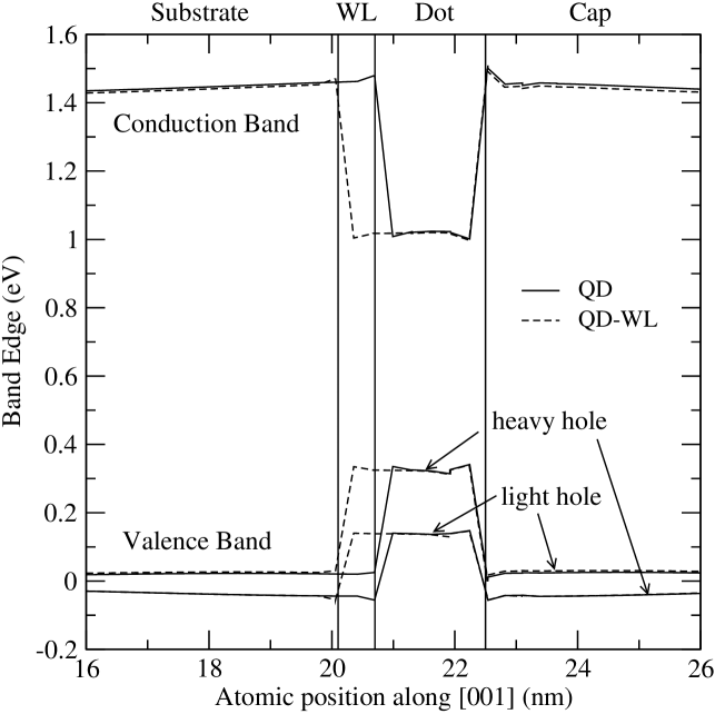
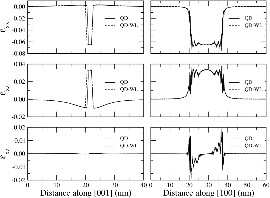
Figure 2 shows the resulting strain profile along the growth direction and in the growth plan (see lines and in Fig. 1). The strain penetrates into the GaAs buffer as deeply as 15 nm along the growth direction, and as widely as 5 nm in the growth plane. To illustrate the effect of the wetting layer on the strain distribution, the strain profiles of the dot with and without a wetting layer are plotted together in Figure 2. Besides the wetting layer region, the two strain profiles are almost identical within about 1% relative difference. For example, the inclusion of the wetting layer slightly reduces from 0.0333 to 0.0330, and from -0.0653 to -0.0647 at the center of the dot. This small change shows that the strain does not relax efficiently through the thin wetting layer. Figure 2 also shows that shear strain reaches 0.02 near the interface between InAs and GaAs in the growth plane.not (a) Although the interface geometry is different between the QD and the QD-WL structures, their shear strain distribution is almost identical. Overall, the wetting layer does not change the strain distribution in the InAs dot and the GaAs buffer in terms of both hydrostatic/biaxial strain () and shear strain ().
Within the strained structure, we calculate its local potential profile. The potential profile is obtained by computing the band structure for a periodic lattice with the geometry of the local strained unit cell. Figure 3 shows the conduction and valence band edges of each unit cell along the growth direction [001]. The valence band edge of unstrained GaAs is set to be zero as a reference energy. Strain effects are significant on both conduction and valence bands. The conduction band edge in the strained dot shifts up from 0.6 eV (unstrained InAs conduction band edge) to 1.0 eV, while the valence band edge splits to two branches, the heavy- and light-hole bands separated by 0.2 eV. The valence band edge for unstrained InAs is 0.23 eV. The order of the heavy- and light-hole bands in the dot is opposite the order in the buffer, because the biaxial components () of the dot strain and the buffer strain have an opposite sign.
The difference in the potential profiles for a quantum dot without a wetting layer (QD) and a dot with a wetting layer (QD-WL) is illustrated in Figure 3. The inclusion of the wetting layer extends the width of the confining potential well, but hardly modifies the height of the potential well. The change in the potential height is about 1 meV. The small change is consistent with the small difference in their strain profiles. Due to the change of the material, the potentials in the wetting layer region differ by 0.44 eV for the conduction band, and by 0.36 eV for the heavy hole band.
| Structure | |||||
|---|---|---|---|---|---|
| QD | 1.378 | 0.158 | 1.220 | 0.042 | 0.025 |
| QD-WL | 1.314 | 0.204 | 1.110 | 0.042 | 0.022 |
| QD-Disk | 1.337 | 0.192 | 1.145 | 0.047 | 0.024 |
| QD-WL-Approx | 1.334 | 0.180 | 1.154 | 0.043 | 0.022 |
We next calculate the confined single-particle energies for the QD and QD-WL structures. The single-particle energies are calculated with a truncated GaAs buffer (30 x 30 x 15 nm box) instead of the large GaAs buffer (60 x 60 x 40 nm box) used for the strain calculation. This method takes an advantage of the spatial localization of the confined states, and significantly reduce the required computation time. An energy convergence of 1 meV is obtained by varying the truncated buffer size. To eliminate spurious surface states in the artificially truncated buffer, the dangling-bond energies of surface atoms are raised by 10 eV.Lee et al. (2004) This surface treatment efficiently eliminates all the spurious surface states without changing the confined states of interest.Lee et al. (2004)
Table 1 lists the calculated single particle energies relative to the GaAs valence band edge. As the wetting layer is included, the lowest electron energy shifts down by 64 meV and the highest hole energy shifts up by 46 meV, leading to the reduction of the energy gap by 110 meV (9% relative change). As a first-order effect, these shifts are attributed to an increase of the width of the confinement potential in the vertical direction [001]. To estimate the effect of the width change, we calculate the single-particle energies for a quantum dot with a disk beneath the dot (QD-Disk). The disk thickness is the same as the thickness of the wetting layer. The energies of QD-Disk are closer to those of QD-WL than to those of QD. The difference between the energies of QD-Disk and QD-WL is attributed to the wetting layer region beyond the disk region.
As another approximation for the wetting layer effect, we calculate the first-order correction due to the potential change in the wetting layer region (QD-WL-Approx) as follows.
| (5) | |||||
| (6) |
Here, is the operator that projects the wave function onto the wetting layer region, and and are the electron and hole wave functions obtained with the QD structure. Factors 0.44 eV and 0.36 eV are the shift of the effective electron and hole potential energy in the wetting layer region, respectively. The resulting energies differ from the QD-WL energies by about 20 meV. The relatively large energy difference between QD-WL-Approx and QD-WL suggests that the wave function of QD is considerably different from that of QD-WL.
| Electron | Hole | |||||
|---|---|---|---|---|---|---|
| Structure | Dot | WL | Buffer | Dot | WL | Buffer |
| QD | 0.43 | 0.10 | 0.47 | 0.82 | 0.06 | 0.12 |
| QD-WL | 0.43 | 0.15 | 0.42 | 0.72 | 0.17 | 0.11 |
In addition to the energy gap, we also analyze the effect of the wetting layer on the energy spacings between the electrons levels () and between the hole levels (). As listed in Table 1, remains the same, while changes by 3 meV (12% relative change). The energy spacings between the ground and excited electron (or hole) level are determined mainly by the lateral confinement rather than the vertical confinement, because lens-shaped self-assembled quantum dots have a large aspect ratio. No change in suggests that the wetting layer does not change the effective lateral confinement range for the electron. In contrast, the decrease of suggests that the wetting layer increases the lateral confinement range for the hole.
We further study the energy gap and spacing change with respect to the ratio of the dot height to the wetting-layer height. For a quantum dot with a larger height (4 nm) and the same base diameter (18 nm), the inclusion of the wetting layer (still 2 ML thick) leads to the change of the gap from 1.103 eV to 1.050 eV (5% change), from 0.051 eV to 0.047 eV (8% change), and from 0.023 eV to 0.019 eV (17% change). In comparison to the small dot discussed above (see Table 1), the change in the gap is smaller for the large dot, while the change in the spacing is larger. This illustrates that the effect of the wetting layer on the energy gap and spacing is sensitive to the height ratio . The smaller change in the gap can be explained by the small relative change in the confinement potential width in the vertical direction. The larger change in the spacing is related to the fact that the electron and hole are more localized in the large dot than in the small dot. When the wetting layer is included, the localized wave functions spread to the wetting layer, leading to a larger spatial extent in the lateral direction and thus to a small energy spacing.
Finally, since the wetting layer provides an extra space for the electron and hole to be confined, we investigate how the electron and hole wave functions respond to the extra space. The change in the wave functions is analyzed in two ways. First, the wave functions are integrated in three regions: the dot, the wetting layer, and the buffer. Table 2 lists the resulting weights in the three regions. The electron wave function is weakly confined in the dot region, whereas the hole wave function is strongly confined in the dot. The difference between the electron and hole wave function distributions is related to the light electron mass and the heavy hole mass. When the wetting layer is included, the electron wave function shifts from the buffer to the wetting layer. In contrast, the hole wave function shifts from the dot to the wetting layer. We find that for the large dot discussed above (height 4 nm), the electron wave function becomes more confined in the dot region and hence the effect of the wetting layer on the electron wave function distribution becomes similar to that on the hole wave function. This shows that the shift trend of the wave function due to the wetting layer is related to the degree of the localization of the wave function.
| Structure | State | ||||
|---|---|---|---|---|---|
| QD | Electron | 4.99 | 3.29 | 1.75 | 0.71 |
| QDWL | Electron | 4.97 | 3.36 | 1.54 | 0.41 |
| QD | Hole | 3.43 | 2.37 | 0.70 | 0.75 |
| QDWL | Hole | 3.89 | 2.70 | 0.73 | 0.45 |
Second, the spatial extents of the wave functions are evaluated with , , and , where is the center of mass given by . The calculated expectation values are listed in Table 3. The spatial extent of the electron function is relatively unchanged, while the extent of the hole wave function increases by 0.46 nm. These trends are consistent with the wave function weight shifts listed in Table 2. The hole wave function spreads from the dot to the wetting layer, leading to a larger spatial extent in both lateral and vertical dimensions. In contrast, the electron wave function moves from the buffer to the wetting layer, leading to a smaller spatial extent in the vertical dimension and a larger spatial extent in the lateral dimension.
We also observe from the center of mass that both the electron and hole wave function move toward the bottom of the dot by 0.3 nm, when the wetting layer is included. However, the relative distance between the electron’s and hole’s center of mass is unchanged. For both QD and QD+WL, the hole’s center of mass is above the electron’s by 0.04 nm, which was observed by a Stark effect experimentet al. (2000) and also predicted by an empirical psudopotential calculation.Shumway et al. (2001) It is interesting to note that an eight-band calculation predicts the opposite electron-hole alignment.Sheng and Leburton (2001a) The model produces the measured alignment, hole above electron, only when gallium diffusion is introduced near the top of the dot.Sheng and Leburton (2001a)
IV Discussion and Conclusion
In summary, the effect of wetting layers on the strain and electronic structure of InAs self-assembled quantum dots is investigated with an atomistic valence-force-field model and an empirical tight-binding model. By comparing a dot with and without a wetting layer, we find that the inclusion of the wetting layer weakens the strain inside the dot by only 1% relative change while it reduces the energy gap between the confined electron and hole states by as much as 10%.
The small change in the dot strain indicates that strain relaxes little through the thin wetting layer. Overall, the wetting layer does not change the strain distribution in the self-assembled quantum dot. As a consequence, we speculate that the phonon spectrum of the quantum dots can be efficiently modeled without including a wetting layer, since the phonon spectrum is modified from the bulk spectrum predominantly due to strain rather than size quantization.Artus et al. (2000); Ibanez et al. (2003); Grundmann et al. (1995); Groenen et al. (1999); not (b)
The large reduction of the energy gap in the quantum dot with a wetting layer is attributed to the increase in the width of the confining potential rather than the change in the height of the potential. First order perturbation calculations or, alternatively, the addition of an InAs disk below the quantum dot confirm this conclusion. In a thin quantum dot, the effect of the wetting layer on the wave function is qualitatively different for the weakly confined electron and the strongly confined hole states. The electron wave function moves from the buffer to the wetting layer, while the hole wave function spreads from the dot to the wetting layer region. The redistribution of the wave function causes a decrease in the hole level spacing , since the effective lateral confinement range of the hole increases.
Since the wetting layer considerably affects both the single-particle energy and wave function, the wetting layer is also expected to influence the electrical and optical properties of self-assembled quantum dots. For example, the overlap between the electron and hole wave function in the wetting layer increases fourfold when the wetting layer is included (see Table. 2). This will lead to different oscillator strengths and photoluminescence polarization for inter-band transitions. Furthermore, the spatial extent of the hole wave function increases, while that of the electron wave function remains the same (see Table. 3). This will lead to a weaker excitonic binding energy. Finally, the spatial extents of the wave functions in the vertical direction determines the coupling between stacked quantum dots. When the wetting layer is included, the vertical extent of the hole wave function increases, while that of the electron wave function decreases (see Table 3). This will lead to a larger inter-dot coupling for hole levels but a smaller inter-dot coupling for electron levels. Therefore, in order to accurately model the electric and optical properties of a single self-assembled dot and coupled quantum dots, the wetting layer should be included in the model.
Acknowledgements.
This work was performed at the Jet Propulsion Laboratory, California Institute of Technology under a contract with the National Aeronautics and Space Administration. Funding was provided under grants from ARDA, JPL Bio-Nano program, and NSF (grant No. EEC-0228390). One of the authors (O.L.L.) held a National Research Council Research Associateship Award at JPL.References
- Bimberg et al. (1999) D. Bimberg, M. Grundmann, and N. Ledentsov, eds., Quantum Dot Heterostructures (Wiley, New York, 1999).
- Califano and Harrison (2000) M. Califano and P. Harrison, Phys. Rev. B 61, 10959 (2000).
- Williamson et al. (2000) A. J. Williamson, L.-W. Wang, and A. Zunger, Phys. Rev. B 62, 12963 (2000).
- Williamson and Zunger (1999) A. J. Williamson and A. Zunger, Phys. Rev. B 59, 15819 (1999).
- Pryor (1999) C. Pryor, Phys. Rev. B 57, 7190 (1998).
- Pryor (1999) C. Pryor, Phys. Rev. B 60, 2869 (1999).
- Sheng and Leburton (2001a) W. Sheng and J.-P. Leburton, Phys. Rev. B 63, 161301 (2001a).
- Sheng and Leburton (2001b) W. Sheng and J.-P. Leburton, Phys. Rev. B 64, 153302 (2001b).
- Sheng and Leburton (2003) W. Sheng and J.-P. Leburton, Phys. Rev. B 67, 125308 (2003).
- Pryor and Flatte (2003) C. E. Pryor and M. E. Flatte, Phys. Rev. Lett. 91, 257901 (2003).
- Grundmann et al. (1995) M. Grundmann, O. Stier, and D. Bimberg, Phys. Rev. B 52, 11969 (1995).
- Wang et al. (1999) L.-W. Wang, J. Kim, and A. Zunger, Phys. Rev. B 59, 5678 (1999).
- Groenen et al. (1999) J. Groenen, C. Priester, and R. Carles, Phys. Rev. B 60, 16013 (1999).
- Fonseca et al. (1998) L. R. C. Fonseca, J. L. Jimenez, J. P. Leburton, and R. M. Martin, Phys. Rev. B 57, 4017 (1998).
- Stier et al. (1999) O. Stier, M. Grundmann, and D. Bimberg, Phys. Rev. B 59, 5688 (1999).
- Shumway et al. (2001) J. Shumway, A. J. Williamson, A. Zunger, A. Passaseo, M. DeGiorgi, R. Cingolani, M. Catalano, and P. Crozier, Phys. Rev. B 64, 125302 (2001).
- Santoprete et al. (2003) R. Santoprete, B. Koiller, R. B. Capaz, P. Kratzer, Q. K. K. Liu, and M. Scheffler, Phys. Rev. B 68, 235311 (2003).
- Keating (1966) P. Keating, Phys. Rev. 145, 637 (1966).
- Martin (1970) R. M. Martin, Phys. Rev. B 1, 4005 (1970).
- Pryor et al. (1998) C. Pryor, J. Kim, L. W. Wang, A. J. Williamson, and A. Zunger, J. of Appl. Phys. 83, 2548 (1998).
- Madelung (1996) O. Madelung, ed., Semiconductors-Basic Data (Springer, New York, 1996), 2nd ed.
- Boykin et al. (2002) T. B. Boykin, G. Klimeck, R. C. Bowen, and F. Oyafuso, Phys. Rev. B 66, 125207 (2002).
- Klimeck et al. (2002) G. Klimeck, F. Oyafuso, T. B. Boyking, R. C. Bowen, and P. von Allmen, Computer Modeling in Engineering and Science 3, 601 (2002).
- Moison et al. (1994) J. M. Moison, F. Houzay, F. Barthe, L. Leprince, E. André, and O. Vatel, Appl. Phys. Lett. 64, 196 (1994).
- Kobayashi et al. (1996) N. P. Kobayashi, T. R. Ramachandran, P. Chen, and A. Madhukar, Appl. Phys. Lett. 68, 3299 (1996).
- Mukahametzhanov et al. (1999) I. Mukahametzhanov, J. Wei, R. Heitz, and A. Madhukar, Appl. Phys. Lett. 75, 85 (1999).
- Solomon et al. (1996) G. S. Solomon, J. A. Trezza, A. F. Marshall, and J. S. Harris, Phys. Rev. Lett. 76, 952 (1996).
- Artus et al. (2000) L. Artus, R. Cusco, S. Hernandez, A. Patane, A. Polimeni, M. Henini, and L. Eaves, Appl. Phys. Lett. 77, 3556 (2000).
- Oyafuso et al. (2003) F. Oyafuso, G. Klimeck, P. von Allmen, and T. B. Boykin, Phys. Status Solidi B 239, 71 (2003).
- not (a) The 2% shear strain raises a question about the validity of our VFF model which has a 10 – 20% deviation of from the experimental value. However, the shear strain is localized near the interface and the biaxial strain is overall dominant in the self-assembled dot.
- Lee et al. (2004) S. Lee, F. Oyafuso, P. von Allmen, and G. Klimeck, Phys. Rev. B 69, 045316 (2004).
- et al. (2000) P. W. F. et al., Phys. Rev. Lett. 84, 733 (2000).
- not (b) In contrast, the size quantization effect on the phonon spectrum is important in chemically synthesized nanocrystals, where strain is weak and the typical size is a few nanometers.
- Ibanez et al. (2003) J. Ibanez, A. Patane, M. Henini, L. Eaves, S. Hernandez, R. Cusco, L. Artus, Y. G. Musikhin, and P. N. Brounkov, Appl. Phys. Lett. 83, 3069 (2003).