Spin Hall Effect in p-type Semiconductors
Abstract
The spin Hall effect is a phenomenon of inducing spin current by an external electric field. We recently proposed that this effect can occur in p-type semiconductors without relying upon any disorder scattering [S. Murakami et al., Science 301, 1348 (2003)]. This intrinsic effect is due to the “Berry phase in momentum space”, representing topological structure of the Bloch band structure. We explain how the Berry phase brings about the spin Hall effect, and review several interesting aspects of this effect.
1 Introduction
In the emerging spintronics[1, 2] technology, one of the important issues is to understand the dynamics of spins in metals and semiconductors. In realizing semiconductor spintronics devices such as Datta-Das spin transistor [3], the spin dynamics is vital for effective spin injection/detection, and spin manipulation. In this context one of the recent remarkable findings is the proposals of the intrinsic spin Hall effect. In the spin Hall effect, an external electric field induces a spin current perpendicular to the field. This effect has been considered to arise extrinsically, i.e. by impurity scattering. The scattering becomes spin-dependent in the presence of the spin-orbit coupling, and it results in the spin Hall effect. In contrast, it has been recently predicted that the spin Hall effect can arise intrinsically. It has been proposed for two systems independently, one is for n-type semiconductors by the authors [4, 5], and the other is for two-dimensional p-type semiconductors in heterostructure by Sinova et al.[6] This intrinsic spin Hall effect has theoretically interesting aspects similar to the quantum Hall effect, and it might be useful for effective spin injection into semiconductors without using magnetic field.
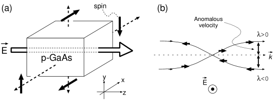
The spin Hall effect by the electric field along the -axis is generally written as , where denotes the current of the -th component of the spin flowing toward the -axis (see Fig. 1 (a)). Because both the spin current and the electric field are even under time-reversal symmetry, the spin Hall conductivity is also even. This represents a reactive (nondissipative) response of the system. This is to be contrasted with usual longitudinal charge conductivity ; it is odd under time-reversal, representing a dissipative response. We also note that because is even under time-reversal, it can be nonzero even in nonmagnetic materials. The criterion for nonzero spin Hall conductivity will be discussed later.
2 Berry phase in momentum space
The spin Hall effect can be attributed to “Berry phase in momentum space”. Berry phase is a geometrical phase associated with an adiabatic change of the system[7]. Suppose the Hamiltonian depends on some parameter, and the parameter adiabatically changes to go back to its initial value at the end. The energy levels are assumed to be non-degenerate. If we assume that the initial state is an eigenstate, the final state is also the same eigenstate, multiplied by an extra phase factor. This phase factor is called the Berry phase. In many contexts this Berry phase comes into physical phenomena. For details see Ref. \refciteshaperewilczek-niu.
In solid state physics, one of the important choices for this parameter is the wavevector . This “Berry phase in momentum space” has been studied in the context of quantum Hall effect and also of anomalous Hall effect. To put it briefly, the intrinsic piece of the Hall conductivity is determined by a vector field , characterizing topological structure of the Bloch band. This vector field is called a Berry curvature, and it is defined as , where
| (1) |
with a periodic part of the Bloch wavefunction . From the Kubo formula, the intrinsic Hall conductivity is expressed as
| (2) |
where is a band index and the integral is over the whole Brillouin zone, is the -component of the vector , and is the Fermi distribution function for the -th band.
There is an alternative way to see why this Berry curvature contributes to . Sundaram and Niu[9] formulated semiclassical equations of motion including the effect of Berry phase. The resulting equations are given by
| (3) | |||
| (4) |
The second term in Eq. (3) represents an anomalous velocity coming from the Berry phase. Without this term, this set of equations is the conventional one in Boltzmann transport theory. This anomalous velocity gives rise to the intrinsic Hall conductivity as shown below. First, we note that the current is expressed as
| (5) |
where is a distribution function. In the thermal equilibrium vanishes; a change in or gives rise to nonzero current. Ohmic current comes from the deviation of from its equilibrium distribution , and is carried by electrons near the Fermi surface. In contrast, the anomalous velocity from the Berry phase (the second term in Eq. (3)), when plugged into Eq. (5), amounts to an anomalous current with the following novel properties; (i) all the occupied states contribute to the current, and (ii) the current accompanies no dissipation. This anomalous velocity is perpendicular to the applied electric field, and appear as a Hall effect. The resulting formula reproduces Eq. (2) obtained by the Kubo formula.
Because of a remarkable similarity between Eqs. (3), (4), the Berry curvature can be regarded as a “magnetic field in -space”, and then corresponds to a “vector potential in -space”. We note that this Berry curvature can have monopoles[10, 11, 7, 12]. The monopole density is written as , where is an integer. As conveys topological properties of the Bloch wavefunctions, it is natural to ask what corresponds to the locations of the monopoles. The answer is the degeneracy points in space, where the -th band touches other bands[7]. Because the field is radiated from such monopoles, the magnitude of tends to be larger for nearer to the monopoles. The author recently proposed that such monopoles in momentum space affects gap functions in magnetic superconductors[11]. First-principle calculations of well explain experimental data of anomalous Hall effect[10, 13].
3 Semiclassical theory of the spin Hall effect in p-type semiconductors
Let us formulate this semiclassical transport theory for p-type semiconductors. For semiconductors with diamond or zincblende structures, the valence bands consist of two doubly-degenerate bands, i.e. the light-hole (LH) and the heavy-hole (HH) bands. These two bands are described by the following Luttinger Hamiltonian
| (6) |
where are spin matrices. Here we have neglected a tiny contribution coming from breaking of inversion symmetry in the zincblende structure. The helicity is a good quantum number, and it can take and corresponding to the HH and the LH bands, respectively.
The semiclassical equations of motion for holes under an electric field read as
| (7) |
from Eqs. (3)(4). Here is an eigenenergy for the band with helicity . The Berry curvature is given by , which depends on the helicity. This curvature, i.e. the flux density, corresponds to a field radiated from a monopole at with strength , reflecting that the two bands are degenerate at . To capture the features of the anomalous velocity from the Berry phase, we show in Fig. 1 (b) the trajectories of holes projected onto a plane perpendicular to the electric field[14]. If there is no anomalous velocity, the holes will move parallel to . The Berry curvature gives rise to an anomalous velocity perpendicular to both and . This anomalous velocity is opposite for opposite helicity, i.e. for opposite spin orientation. This anomalous velocity from the motion along , when summed over all of occupied states, amounts to a spin current. In the zero temperature, by applying an electric field along the -direction, the spin current in which spins along the -axis will flow along the -direction is calculated as
| (8) |
Here, and are the Fermi wavenumbers for the HH and the LH bands, respectively. A schematic of this effect is shown in Fig. 1 (a).
Let us express the above proportionality constant (spin Hall conductivity) as so that shares the same unit as the usual charge conductivity . In GaAs at room temperature, a hole density yields , and yields , and . Thus the spin Hall conductivity is as large as or even larger than the usual charge conductivity at room temperature. An energy scale to be compared with the temperature is the energy difference between the two valence bands. If the hole density is as high as , this energy scale is nominally much larger than room temperature, and we expect that even at room temperature the spin current will remain measurably large.
4 Physics of the spin Hall effect
We can discuss a criterion for appearance of the spin Hall effect. The spin Hall effect is essentially caused by the spin-orbit coupling. The spin-orbit coupling brings about a splitting of bands into multiplets of . If all the multiplets split by the spin-orbit coupling are filled, the spin Hall effect cancels completely. Therefore, the criterion for the nonzero spin Hall effect is a difference of fillings within the same -multiplet. Many kinds of materials, among metals and even band-insulators, can satisfy this criterion; hence, the spin Hall effect should be quite a common phenomenon, whereas the size of the effect may vary.
Let us take a few examples to see how this criterion works. For the valence band of semiconductors, hole-doping gives rise to different fillings between the HH and LH bands, and the spin Hall effect emerges as the criterion tells us. On the other hand, the conduction band is doubly degenerate. Therefore, electron-doping does not give rise to the spin Hall effect. In contrast, if we make heterostructures from n-type semiconductors, the Rashba term induces the splitting, and results in the spin Hall effect. Indeed, the spin Hall effect is nonzero as predicted by Sinova et al.[6]. Interestingly, the spin Hall effect in this case takes a universal value , independent of the strength of the Rashba coupling.
So far we assumed an absence of any disorder. In reality we cannot escape from disorder and impurities, and it is important to clarify the disorder effect. There have been several works on this issue, which are mainly on randomly distributed spinless impurities with a short-ranged potential. For the p-type semiconductors with spinless impurities, the self-energy and the vertex correction is calculated within the Born and the ladder approximation. The self-energy turns out to be a constant, and the vertex correction identically vanishes[15]. This suggests that in the clean limit the spin Hall conductivity reproduces the intrinsic value calculated earlier[4].
In contrast, in the 2D n-type semiconductors in heterostructures, it is still controversial even for spinless impurities. Inoue et al. calculated the self-energy and the vertex correction within the Born and ladder approximation [16]. Remarkably, they showed that with the vertex correction, the spin Hall effect becomes zero in the clean limit, as opposed to the intrinsic value [6]. Nevertheless, there are two numerical calculations which contradict this analytical result. One is based on Kubo formula[17], and the other is on the Landauer-Büttiker formalism[18]. These two calculations suggest that in the clean limit the spin Hall conductivity reproduces the intrinsic value . This contradiction remains to be resolved.
We also mention another theoretical issue, concerning a definition of the spin current. In the presence of the spin-orbit coupling, as in the present problem, the spin is not conserved; hence, a spin current cannot be uniquely defined. In such cases, the spin current is not necessarily defined as , where is an anticommutator. There is no (mathematically) unique definition, and it is rather a physics problem as to which definition is suitable for realistic measurement. On physical grounds, we have given one reasonable choice for the definition of the spin current [5]. For details see Ref. \refcitemurakami2003c.
At present an unambiguous detection of the spin Hall effect has still to come. One reason is because detection of spin current is not easy in general. A usage of ferromagnetic electrodes for detection would bring about a Hall effect from the fringing field, and one has to separate it from the spin Hall effect. On the other hand, the simplest geometry of spin-LED structure does not work efficiently, because the spins in the induced spin current is parallel to the layers[19]. An ingenious experimental setup is highly desired.
5 Conclusion
In this paper, we briefly review the theoretical predictions of the intrinsic spin Hall effect, as a manifestation of the Berry phase in momentum space. Though there remain some theoretical and experimental issues to be clarified, the spin Hall effect should consititute an important part in understanding the spin dynamics in semiconductors and in implementing spintronics devices.
Acknowledgments
This work is in collaboration with N. Nagaosa and S. C. Zhang, and the author would like to thank them for fruitful discussions and helpful comments. This work is supported by Grant-in-Aids from the Ministry of Education, Culture, Sports, Science and Technology of Japan.
References
- [1] G. A. Prinz, Science 282, 1660 (1998).
- [2] S. A. Wolf, D. D. Awschalom, R. A. Buhrman, J. M. Daughton, S. von Molnár, M. L. Roukes, A. Y. Chtchelkanova, and D. M. Treger, Science 294, 1488 (2001).
- [3] S. Datta and B. Das, Appl. Phys. Lett. 56, 665 (1990).
- [4] S. Murakami, N. Nagaosa, and S. C. Zhang, Science 301, 1348 (2003).
- [5] S. Murakami, N. Nagaosa, and S. C. Zhang, cond-mat/0310005, to appear in Phys. Rev. B.
- [6] J. Sinova, D. Culcer, Q. Niu, N. A. Sinitsyn, T. Jungwirth, and A. H. MacDonald, Phys. Rev. Lett. 92, 126603 (2003).
- [7] M. V. Berry, Proc. R. Soc. London, Ser. A 392, 45 (1984).
- [8] A. Shapere and F. Wilczek, Geometric Phases in Physics (World Scientific, Singapore, 1989); A. Bohm, A. Mostafazadeh, H. Koizumi, Q. Niu and J. Zwanziger, The Geometric Phase in Quantum Systems (Springer, Berlin, 2003).
- [9] G. Sundaram and Q. Niu, Phys. Rev. B 59, 14915 (1999).
- [10] Z. Fang, N. Nagaosa, K. S. Takahashi, A. Asamitsu, R. Mathieu, T. Ogasawara, H. Yamada, M. Kawasaki, Y. Tokura, and K. Terakura, Science 302, 92 (2003).
- [11] S. Murakami and N. Nagaosa, Phys. Rev. Lett. 90, 057002 (2003).
- [12] G. E. Volovik, JETP Lett. 46, 98 (1987).
- [13] Y. Yao, L. Kleinman, A. H. MacDonald, J. Sinova, T. Jungwirth, D. S. Wang, E. Wang, and Q. Niu, Phys. Rev. Lett. 92, 037204 (2004).
- [14] In reality, the holes will be scattered by disorder before they run a long way along this trajectory.
- [15] S. Murakami, cond-mat/0405001.
- [16] J. Inoue, G. E. W. Bauer, L. W. Molenkamp, cond-mat/0402442.
- [17] K. Nomura, private communications.
- [18] Y. Xiong, X. C. Xie, cond-mat/0403083.
- [19] Z. G. Yu, W. H. Lau, M. E. Flatté, cond-mat/0308220.