Spin filtering through a double-bend structure
Abstract
We propose a simple scheme for the spin filter by studying the coherent transport of electrons through a double-bend structure in a quantum wire with a weak lateral magnetic potential which is much weaker than the Fermi energy of the leads. Extremely large spin polarized current in the order of micro-Ampere can be obtained because of the strong resonant behavior from the double bends. Further study suggests the roubustness of this spin filter.
pacs:
85.75.-d, 73.23.Ad, 72.25.-bThe rapid emerging field of spintronics promises to provide new advances that have a substantial impact on future applications.prinz ; loss ; spin Effective and efficient electrical spin injection of spin-polarized current into semiconductors is one of the major challenges in this field.wolf ; mon ; filip One method is to inject spin current through ideal ferromagnet/semiconductor interface. However, the polarization of the injected current is rather small due to the large conductivity mismatch.schmidt The use of spin filters is therefore an alternative approach which can significantly enhance spin injection efficiencies. In some previous works, spin-selective barriers gilbert or stubs stub are essential to realize spin polarization (SP). Other methods such as quantum dotfran and resonant tunneling diode koga also have been reported. Very recently we also proposed a scheme of spin filter by utilizing the “band-gap” generated by the weak lateral magnetic modulations.wu However, it is noted that the spin currents of these filters are relatively small.
In this letter we propose a new scheme of the spin filter which provides exteramly large spin current by utilizing the resonance in a double-bend structure with a uniform small magnetic field which can be realized by sticking a magnetic strip on top of the sample or using magnetic semiconductor. The effect of the bend discontinuity has been discussed in detail in a mode-matching theory by Weisshaar et al.wei There it was shown that strong resonance effects are present in the transmission coefficient versus energy due to the presence of a perpendicular single right bend. They further showed that the effect of the second bend (i.e. a double-bend structure) is to add further fine resonances superimposed on the dominant resonance, with the width and the spacing in energy depending on the cavity of length . We will show that this resonance effect can be effectively utilized to generate SP’s.
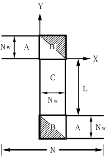
A schematic of the double-bend structure is shown in Fig. 1. The spin dependent potential with Zeeman-like form is applied on the double bends (regions B and C). Here if locates at regions B and C , and 0 otherwise. is for spin-up and -down electrons, respectively. denotes a spin-independent parameter for the strength of the potential. For , spin-up and -down electrons experience different potentials: the spin-up electrons coherently transport through a “transparent” barrier while the spin-down ones do through a well. Therefore, spin polarized current can be obtained because of the mismatch of the resonances from the double bends of the spin-up and -down electrons.
We describe the double-bend structure by a tight-binding Hamiltonian with the nearest-neighbour approximation:
| (1) | |||||
in which and denote the coordinates along the - and -axis respectively. () when locates at the B and C regions (when locates at the A region), denotes the on-site energy with . is the hopping energy with and standing for the effective mass and the “lattice” constant respectively.
The spin dependent conductance is calculated using the Landauer-BüttikerBu formula with the help of the Green’s function method.Da The two-terminal spin-resolved conductance is given by with () representing the self-energy function for the isolated ideal leads.Da We choose the perfect ideal ohmic contact between the leads and the semiconductor. and are the retarded and advanced Green functions for the conductor, but with the effect of the leads included. The trace is performed over the spatial degrees of freedom along the -axis. The spin dependent current within an energy window is given by .
We perform a numerical calculation for a quantum wire with width . A hard wall potential is applied in this transverse direction which makes the lowest energy of the th subband (mode) be . Å which makes eV throughout the computation. We take the Zeeman splitting energy .
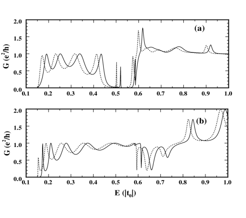
In Fig. 2(a) the conductance is plotted as a function of the Fermi energy of the leads with and cavity length . Both the single and the double modes are included in the figure. It is seen from the figure that SP is obtained from each energy window in which the mismatch of the resonances for electrons with different spin directions occurs. Spin current densities can be obtained from the energy window with nA for spin-up current and from the window with nA for spin-down current, each with 100 % SP. SP can also be obtained from other energy intervals due to the mismatch of the resonance peaks for different spin. Particularly if one chooses the energy window , one gets an extremely large spin current A. This large spin current scales with the magnitude of the applied potential . If one takes an even smaller number (), one also gets a large current A (0.072 A) by choosing a suitable energy window on the edge of the gap.
The spin-independent gap near corresponds to the anti-resonance gap due to the reflection of the bend structure. By cutting off the corners (the shadowed areas in Region B shown in Fig. 1) from the both bends, one can see from Fig. 2(b) that the gap disappears and one also loses the energy window for the large spin current.
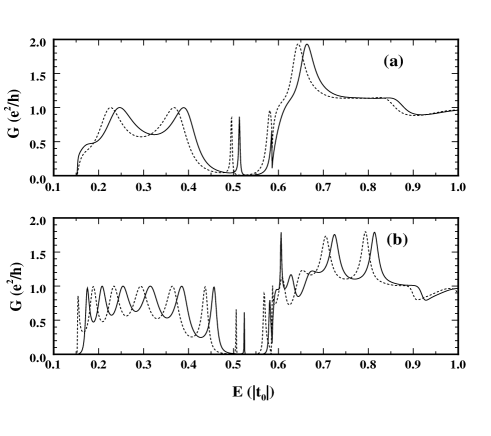
In order to understand the resonance feature of the double bends, we calculate the conductance with and . By comparing Fig. 3 and Fig. 2(a), one finds that the number of the resonant peaks increases with the cavity length . When the wave length of the incident electron satisfies the standing wave condition with , the conductance reaches the maximum. It is therefore easy to see that within the fixed energy interval of the first subband (), a larger bend distance corresponds to a larger and therefore more resonance peaks.
We also check the roubustness of the spin filter proposed above by including Anderson disorder to investigate its effect on the spin polarized currents. We take the strength of the disorder to be , five times of the potential . We still obtain a large spin polarized current A.
Finally we point out that the scheme of the spin filter proposed in this letter can be generalized to any structure in which the conductance oscillates with the energy of the incident electrons. Then by applying a small spin-dependent potential, one gets the mismatch of the resonance peaks for different spins and hence the SP. However, if one wishes to obtain a filter which can give a large spin current, then a anti-resonance gap is essential in the structure.
In summary, we have proposed a simple scheme for spin filter by studying the coherent transport through double-bend structure with a lateral magnetic potential. Extremely large spin current is predicted from this structure. The magnetic potential can be realized by sticking the magnetic strip on top of the sample or using magnetic semiconductors. This spin filter is very robust to the disorder.
One of the authors (MWW) was supported by the “100 Person Project” of Chinese Academy of Sciences and Natural Science Foundation of China under Grant Nos. 9030312 and 10247002.
References
- (1) G. A. Prinz, Phys. Today 48, 58 (1995); Science 282, 1660 (1998).
- (2) D. Loss and D. P. DiVincenzo, Phys. Rev. A 57, 120 (1998).
- (3) Semiconductor Spintronics and Quantum Computation, eds. D. D. Awschalom, D. Loss, and N. Samarth, Springer, Berlin, 2002.
- (4) S. A. Wolf, D. D. Awschalom, R. A. Buhrman, J. M. Daughton, S. von Molnár, M. L. Roukes, A. Y. Chtchelkanova, and D. M. Treger, Science 294, 1488 (2001).
- (5) F. G. Monzon, and M. L. Roukes, J. Mag. Magn. Mater. 198, 632 (1999).
- (6) A. T. Filip, B. H. Hoving, F. J. Jedema, and B. J. van Wees, Phys. Rev. B 62, 9996 (1999).
- (7) G. Schmidt, D. Ferrand, L. W. Molenkamp, A. T. Filip, and B. J. Van Wees, Phys. Rev. B 62, R4790 (2000).
- (8) M. J. Gilbert and J. P. Bird, Appl. Phys. Lett. 77, 1050 (2000); G. Papp and F. M. Peeters, Appl. Phys. Lett. 78, 2148 (2001); J.C. Egues, C. Gould, G. Richter, and L. W. Molenkamp, Phys. Rev. B 64, 195319 (2001).
- (9) X. F. Wang and P. Vasilopoulos, Appl. Phys. Lett. 81, 1636 (2002).
- (10) J. Fransson, E. Holmström, I. Sandalov, and O. Eriksson, Phys. Rev. B 67, 205310 (2003).
- (11) Takaaki Koga, Junsaku Nitta, Supriyo Datta, and Hideaki Takayanagi, Phys. Rev. Lett. 88, 126601 (2002).
- (12) J. Zhou, Q. W. Shi, and M. W. Wu, Appl. Phys. Lett. 84, 365 (2004).
- (13) A. Weisshaar, J. Lary, S. M. Goodnick, and J. K. Tripathi, Appl. Phys. Lett. 55, 2114 (1989); J. C. Wu, M. N. Wybourne, W. Yindeepol, A. Weisshaar, and S. M. Goodnick, Appl. Phys. Lett. 59, 102 (1991).
- (14) M. Büttiker, Phys. Rev. Lett. 57, 1761 (1986).
- (15) S. Datta, Electronic Transport in Mesoscopic Systems (Cambridge University Press, New York, 1995).