Photocurrents in nanotube junctions
Abstract
Photocurrents in nanotube p-n junctions are calculated using a non-equilibrium Green function quantum transport formalism. The short-circuit photocurrent displays band-to-band transitions and photon-assisted tunneling, and has multiple sharp peaks in the infrared, visible and ultraviolet ranges. The operation of such devices in the nanoscale regime leads to unusual size effects, where the photocurrent scales linearly and oscillates with device length. The oscillations can be related to the density of states in the valence band, a factor that also determines the relative magnitude of the photoresponse for different bands.
pacs:
85.60.-q, 72.40.+w, 73.63.Fg, 78.67.ChSince their discoveryIijima , Carbon Nanotubes (NTs) have been the subject of intensive research due to their intriguing electronic and structural properties, and have demonstrated great promise for future nano-electronic devicesnano . However, their potential for opto-electronic applications has received much less attention, despite the ideal properties that NTs present. Indeed, a desirable property of opto-electronic materials is a direct band-gap, since it allows optical transitions to proceed without the intervention of phonons. NTs are unique in this aspect, since all the bands in all semiconducting NTs have a direct gap. Furthermore, the low dimensionality of NTs leads to a diverging density of states at the band edge and a high surface-to-volume ratio, reducing the sensitivity to temperature variations and allowing efficient use of the material. Finally, non-radiative transitions can significantly reduce the performance of conventional materials; NTs are believed to have low defect density, reducing non-radiative transitions.
These unique properties of NTs are only starting to be explored for opto-electronics. Recent experimental workmisewich has shown that NT field-effect transistors can emit polarized light, while illumination of these and other NT devices generates significant photocurrentfreitag ; narkis . Such observations have also been made in semiconductor nanowireswang ; duan ; gudiksen . Often, the observed opto-electronic effects are due to the presence of a p-n junction, with various physical realizations (electrostatically definedmisewich ; freitag , crossed-wire geometryduan , or modulated chemical dopinggudiksen .) Modulated chemical doping of individual semiconducting single-wall NTs to create “on-tube” p-n junctions has recently been reported in the literaturezhou . These NT p-n junctions serve as excellent testbeds for understanding opto-electronics at reduced dimensionality.
Here we show that in simple NT p-n junctions, the photocurrent shows unusual features. Unlike traditional devices, the photoresponse in the NT junctions consists of multiple sharp peaks, spanning the infrared, visible and ultraviolet ranges. Furthermore, at nanoscale dimensions, the NT junctions show size effects, where the photocurrent scales and oscillates with device length.
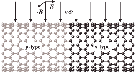
We consider a NT p-n junction under illumination, as shown in Fig. 1. We use a (17,0) single-wall, semiconducting NT of radius 0.66 nm, and model the doping as in Ref. leonard . Our tight-binding Hamiltonian with one orbital per carbon atom and nearest-neighbor matrix element of 2.5 eV gives a direct band-gap for this NT of 0.55 eV. The incident light is assumed to be monochromatic, with polarization parallel to the NT axis.
To calculate the photocurrent, we use a non-equilibrium Green function formalism Datta , in a real-space representation. The device consists of an illuminated scattering region connected to two dark semi-infinite leads, which are also doped (17,0) NTs. The structure of the (17,0) NT corresponds to parallel rings of 17 atoms, which are spaced by nm and nm. Each ring forms a layer in our system, with the rings in the scattering region labelled from to .
Since only layers and couple with the leads, the steady-state, time-averaged current can be written as
| (1) |
(This expression assumes that the hole current is equal and opposite to the electronic current and that the coupling of layers and to the leads is . The appropriateness of this equation for time-dependent Hamiltonians is discussed in Ref. anantram ) Here, and cross the scattering region boundary. To relate these terms to calculated entirely in the scattering region, we use the Dyson equationslake and . (We also note that in the presence of electron-photon interactions and the potential step in the p-n junctionanantram , , an equality that would normally hold for a system without inelastic scattering.)
In the scattering region, is determined from the equations
| (2) |
and
| (3) |
where is the Hamiltonian for the NT p-n junction under illumination. The functions and represent the interaction of the scattering region with the semi-infinite (17,0) NT leads and the incident light. In the presence of the electron-photon interaction, these functions depend on , and the equations are coupled and non-linear. To simplify the calculation, we perform an expansion to first order in the light intensity: , , and , where the order zero functions represent the dark p-n junction. In the absence of an applied bias, the only current in the device is the photocurrent
| (4) |
where
| (5) | |||||
Here , with the Hamiltonian and the self-energy function describing the p-n junction without incident light, including the electrostatic potential. (The Hamiltonian matrix elements are , , and , where is the electrostatic potential on layer ). The self-energies due to the semi-infinite leads are calculated using a standard iterative approachsancho , and where is the Fermi function. The electrostatic potential and charge distribution are determined using a self-consistent procedure as in Ref. leonard . The last two terms in Eq. are proportional to , while, as discussed below, the first term is proportional to . As long as the Fermi level is in the bandgap and not too close to the conduction band edge, the ratio is small, so we neglect the last two terms in Eq. . A benefit of this approach is that a model for does not have to be formulated. (Including electron-hole recombination and other multi-photon processes requires going beyond the perturbation scheme introduced here, and is beyond the scope of this paper. At low light intensities, our calculations should provide a reasonable approximation.)
To derive the function due to the electron-photon interaction, we use the interaction Hamiltonian
| (6) |
where is the time-dependent electromagnetic vector potential, is the electronic momentum operator and is the electron mass. Following the procedure of Ref. Henrickson , we obtain
| (7) |
with
| (8) |
In these equations, nm is the smallest ring separation, is the photon energy, is the speed of light and is the permittivity of free space. is the circumferential angular momentum, labeling each of the bands of the NT. Conservation of is enforced, as required for light polarization parallel to the tube axisbozovic . The photon flux represents the strength of the incoming radiation, in units of photons per unit time per unit area. Since the photocurrents calculated in this work are proportional to , we focus on the photoresponse . (This definition of the photoresponse might seem awkward at first, having units of area/photon. However, the unusual size effects in the nanotube devices are more transparent with this definition.) Because , is proportional to .
Figure 2a shows the calculated self-consistent band diagram for the NT p-n junction for a doping of electrons/C atom. The figure shows the conduction and valence band edges of the band with the smallest band gap, , shifted by the local electrostatic potential. The band bending is characterized by a step at the junction and flat bands away from the junction regionleonard2 .
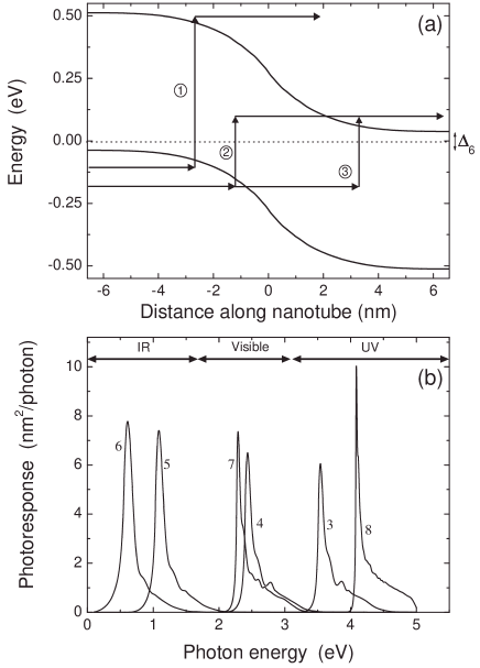
The calculated photoresponse for this device at zero bias when rings are illuminated is shown in Fig. 2b. The photoresponse due to bands (increasing band gap) is separately plotted in the figure (bands are equivalent). The general trend is for the photoresponse for the different bands to peak at higher photon energies as the band gap increases. Because the scattering cross-section decreases with , one would expect the maximum photoresponse attained for each band to decrease with band gap. Surprisingly, the height of the peaks in Fig. 2b does not follow this behavior; in particular the response for band is actually larger than the response for band . This is a result of the different bands having different effective masses. Indeed, the effective mass for is about 36 times larger than for , leading to a much larger density of states near the edge of the valence band. (The role of the density of states will be discussed further below.)
Path 1 in Fig. 2a shows a band-to-band transition with the absorption of a photon of energy . An electron coming from the p-type side of the device in the valence band absorbs a photon and is excited to the conduction band, where it then continues to the n-type terminal. Such a transition is allowed when the photon energy exceeds the band gap ( for band 6). Band-to-band photocurrents in the NT device in the left lead due to electrons coming from the n-type terminal vanish unless the photon energy is larger than the band gap plus the potential step across the junction, in Fig. 2b. This asymmetry in the currents to the left and right terminals leads to the net photocurrents in Fig. 2b.
While these band-to-band transitions explain part of the photoresponse, a significant response exists at energies below the band gap. Such contributions can be attributed to photon-assisted tunneling. Paths 2 and 3 in Fig. 2a show two possible paths for photon-assisted tunneling. For a given band , this process can only occur when , where is the difference between the asymptotic conduction band edge on the p-type side and the asymptotic valence band edge on the n-type side (equal to 0.06 for the band shown in Fig. 2a). The photon-assisted tunneling thus turns on at . As the photon energy increases above , more states in the band gap become available for transport, and the photoresponse increases. For the bands with larger band gaps, the tail due to photon-assisted tunneling is less important relative to the band-to-band peak, since tunneling probabilities decrease with band gap.
The photoresponse of the different bands leads to multiple sharp peaks in three different regions of the electromagnetic spectrum: infrared, visible and ultra-violet. This unusual behavior arises because all the bands in the NT have a direct band-gap, which leads to a response over a wide energy spectrum. The separation of this wide response into peaks grouped in different regions of the electromagnetic spectrum is due to the particular electronic band structure of the NT, which has groups of bands separated by relatively large energies. The conduction band edges for and (infrared response) are separated from those of bands and 7 (visible response) by about 0.6 eV, which are in turn separated by about 0.5 eV from the and conduction band edges (ultraviolet response). Since the photocurrent consists of an excitation from the valence band to the conduction band, the separation in Fig. 2b is twice these values.
In conventional bulk junctions, the photoresponse depends only on the dimensions of the device perpendicular to current flow. The nanotube device however shows a dependence with length, as shown in Fig. 3. Panel (a) in the figure shows the photoresponse of band for different lengths of the illuminated region. As the illuminated region becomes longer, the peak in the photoresponse increases and also moves to lower energies. This behavior leads to linear scaling of the photoresponse with the length of the illuminated region, as the integrated photoresponse in the inset of Fig. 3a shows. The photoresponse for three different photon energies is shown in Fig. 3b. Clearly for (photon-assisted tunneling) the photoresponse saturates with length, due to the fact that the wavefunctions in the band gap decay exponentially away from the junction. The response for and shows a completely different behavior, oscillating around a general linear increase.

These surprising results can be understood from a simplified description of the photocurrent in the nanotube. To this end, we note that the photocurrent density flowing to the right lead can be expressed as
| (9) |
where . (Eq. can be obtained from Eq. by using Dyson’s equation , the relation and the condition that the net current must vanish for the dark junction at zero bias.) At zero bias, is purely imaginary, and therefore so is . The above equation becomes
| (10) |
For a given outgoing electron energy and photon energy , we have found numerically that the argument of the summation is peaked around the diagonal . Taking only these contributions, we obtain
| (11) |
The photocurrent in the NT can thus be understood in terms of the excitation of electrons in each layer along the NT (the term in the above equation), and the subsequent transmission to the lead by .
To explain the linear scaling, we note that for and where is the asymptotic value of the conduction band edge on the p-type side of the device, there is a section of the NT where band-to-band transitions are allowed, and the sum in the last equation is dominated by this section of the NT. As the length of the illumination region is increased, a longer section of the NT is available for band-to-band transitions, leading to the linear scaling of the current with length.
While this explains the linear scaling, there remains the questions of the oscillations in the photoresponse and the dependence of the photoresponse on the effective mass. To address this, we note that contains terms like , which are related to the density of states at layer , , through , with the Fermi function. Therefore, the photocurrent is sensitive to the density of states at energy . This explains the origin of the dependence on the effective mass, and the relative height of the peaks in Fig. 2.
Figure 4 shows the valence band density of states for calculated at layer for systems with illuminated lengths of , , and nm. (This is the density of states near the edge of the illuminated region, which is moving further away from the junction as the length increases). The density of states contains many peaks, and as the system size changes, the peaks move in energy. Because the propagator is sharply peaked at energy , the photoresponse is particularly sensitive to the density of states at . At that energy, the density of states oscillates as a function of the distance from the p-n junction, as illustrated in the inset of Fig. 4. This leads to the oscillations in the photoresponse as a function of illumination length shown in Fig. 3b. The oscillation wavelength of the density of states increases for energies closer to the band edge, causing the different oscillation wavelengths for and in Fig. 3b.

Although the device presented here is fairly simple, it already shows the richness of new phenomena that arises in nanoscale opto-electronics. One may envision several uses for this or related devices (photodetection, power generation, optical communication, etc.), but the important point is that the behavior is much different from traditional devices and must be taken into account in future device development.
This work was supported by the Office of Basic Energy Sciences, Division of Materials Sciences, U.S. Department of Energy under contract No. DE-AC04-94AL85000.
References
- (1) S. Iijima, Nature 354, 56 (1991).
- (2) A. Bachtold et al., Science 294, 1317 (2001); M. S. Fuhrer et al., Science 288, 494 (2000); J. Kong et al., Science 287, 622 (2000).
- (3) J. A. Misewich et al., Science 300, 783 (2003).
- (4) M. Freitag et al., Nano Lett. 3, 1067 (2003).
- (5) T. R. Narkis et al., in preparation.
- (6) J. Wang et al., Science 293, 1455 (2001).
- (7) X. Duan et al., Nature 409, 66 (2001).
- (8) M. S. Gudiksen et al., Nature 409, 66 (2002).
- (9) C. Zhou et al., Science 290, 1552 (2000).
- (10) F. Léonard and J. Tersoff, Phys. Rev. Lett. 85, 4767 (2000).
- (11) S. Datta, Electronic transport in mesoscopic systems (Cambridge University Press, Cambridge, 1995).
- (12) S. Datta and M.P. Anantram, Phys. Rev. B 45, 13761 (1992).
- (13) R. Lake et al., J. Appl. Phys. 81, 7845 (1997).
- (14) M.P. Lopez-Sancho, J.M. Lopez-Sancho, and J. Rubio, J. Phys. F: Metal Phys. 15, 851 (1985).
- (15) L. E. Henrickson, J. Appl. Phys. 91, 6273 (2002).
- (16) I. Božović, N. Božović, and M. Damnjanović, Phys. Rev. B 62, 6971 (2000).
- (17) The detailed properties of dark NT p-n junctions are discussed in F. Léonard and J. Tersoff, Phys. Rev. Lett. 83, 5174 (1999).