Scaling analysis of Schottky barriers at metal-embedded semiconducting carbon nanotube interfaces
Abstract
We present an atomistic self-consistent tight-binding study of the electronic and transport properties of metal-semiconducting carbon nanotube interfaces as a function of the nanotube channel length when the end of the nanotube wire is buried inside the electrodes. We show that the lineup of the nanotube band structure relative to the metal Fermi-level depends strongly on the metal work function but weakly on the details of the interface. We analyze the length-dependent transport characteristics, which predicts a transition from tunneling to thermally-activated transport with increasing nanotube channel length.
pacs:
73.63.-b,73.40.-c,85.65.+hThe nature of Schottky barrier formation and its effect on charge transport through metal-semiconductor interfaces have been actively investigated for decades due to their importance in microelectronics technology, but are not fully resolved despite the tremendous efforts from both the experimental and theoretical sides. MS The rapid development of single-wall carbon nanotubes (SWNT) as a promising device technology functioning at the nano/molecular-scale Dekker99 ; DM ; Avouris presents a new challenge. Xue99 ; TersoffNT ; OdinDe SWNTs are nanometer-diameter all-carbon cylinders. Unlike the planar metal-semiconductor interface, both the contact area and the active device region in a metal-nanotube (NT) interface can have atomic-scale dimensions. In addition, due to the weaker effects of electron-impurity Ando and electron-phonon scattering Phonon ; NTDai in quasi-one-dimensional systems, transport through nanotube junctions can be either coherent or phonon-limited depending on the nanotube type, channel length, temperature and the bias voltage. These have made it difficult to assess the Schottky barrier effect on the measured transport characteristics.
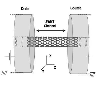
In this paper, we present an analysis of Schottky barrier formation at a model metal-SWNT interface as a function of the SWNT channel length. The model system is illustrated schematically in Fig. 1, where the ends of an infinitely long SWNT wire are buried inside the semi-inifinite metallic electrodes and the channel length is determined by the distance between the source and drain electrodes. NTDai The embedded contact scheme is favorable for the formation of low-resistance contact. DM ; Avouris ; NTDai We choose SWNT as the protype semiconducting SWNT, whose work function is taken as that of the graphite ( eV). DM The SWNT channel length invesitigated ranges from (nm) to (nm), corresponding to number of unitcells of and respectively. We calculate the transport characteristics within the coherent transport regime, as appropriate for such short nanotubes. Phonon ; NTDai We consider gold (Au) and titanium (Ti) electrodes as examples of high- and low- work function metals ( and eV respectively for polycrystalline materials). In view of recent report on ballistic transport in palladium (Pd) contacted SWNT devices, DT03 we also consider Pd electrodes with a similar workfunction to gold ( eV for polycrystalline materials). CRC
We analyze the Schottky barrier effect at the metal-SWNT interface by examining the electrostatics, the band lineup and the conductance of the metal-SWNT wire-metal junction as a function of the SWNT channel length. This is investigated using a Green’s function based self-consistent tight-binding (SCTB) theory, which takes fully into account the three-dimensional electrostatics and the atomic-scale electronic structure of the SWNT junctions. The SCTB model is essentially the semiempirical implementation of the self-consistent Matrix Green’s function (SCMGF) method for ab initio modeling of molecular-scale devices XueMol and has been used previously to investigate Schottky barrier formation when a finite-size SWNT molecule is contacted to the electrodes through the dangling bonds at the end. XueNT
The SCTB model starts with the semi-emprical Hamiltonian of the bare SWNT wire using the Extended Huckel Theory (EHT) with non-orthogonal () basis sets , Hoffmann88 which gives a band gap of . AvouEHT We describe the interaction between the SWNT channel and the rest of the junction using matrix self-energy operators and calculate the density matrix and therefore the electron density of the equilibrium SWNT junction from
| (1) | |||||
| (2) |
Here is overlap matrix and is the Fermi distribution in the electrodes. The matrix self-energy operators include contributions from coupling both with the left (right) electrodes and with the part of the SWNT wire embedded within the left (right) electrode , which are calculated from the surface Green’s function of the semi-infinite metal surfaces and semi-inifinite SWNT wires respectively. XueMol ; Papa86 ; Geometry The Hamiltonian of the SWNT channel is now where is the density of transferred charge and is the induced change in the electrostatic potential.
The self-consistent calculation proceeds by approximating the charge distribution as superposition of atom-centered charge distributions Frau98 , where and is the number of valence electrons on atomic-site of the bare SWNT wire. is a normalized Slater-type function, XueNT ; Frau98 whose exponent is chosen such that , Frau98 where are the atomic electron affinity (ionization potential). This gives , where can be evaluated analytically. XueNT ; Frau98 We take into account the image-potential effect by including within contributions from both atom-centered charges and their image charges (centered around the image positions), rather than imposing an image-type potential correction. The self-consistent cycle is completed by calculating the matrix elements of the potential using two types of scheme: (1) If belong to the same atomic site , we calculate it by direct numerical integration; (2) if belong to different atomic sites, we use the approximation .
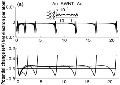
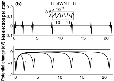
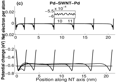
The calculated charge transfer and electrostatic potential change along the cylindrical surface of the SWNT for the Au/Ti/Pd-SWNT-Au/Ti/Pd junctions are plotted in Fig. (2). The electrostatic potential change is the difference between the electrostatic potentials within the SWNT junction and the bare SWNT, obtained as the superposition of contributions from the transfered charges (plus their image charges) throughout the junction. Here it is important to separate the electronic processes at the interface and inside the channel. The coupling with electrodes in the embedded part of the SWNT wire induces only a localized perturbation to the SWNT channel sandwiched between the electrodes, so the electronic states in the middle of the channel are essentially identical to those of the bulk (infinitely long) SWNT except for the shortest (2.1 nm) channel length studied here, leading to similar charge transfer both at the interface and in the middle of the channel. For such SWNT channels (longer than ), the potential change in the middle and consequently the band lineup scheme become independent of the channel lengths. Note that the transfered charge in the middle of the channel shows oscillatory behavior due to the two-sublattice structure of zigzag tubes. XueNT
Compared with the finite SWNT molecule contacted to the electrode surfaces through the ring of dangling-bond end atoms, XueNT the magnitude of charge transfer at the interface is smaller for both the Au-SWNT-Au and Ti-SWNT-Ti junctions since no dangling bonds are involved in the embedded contact scheme. But the magnitudes of both the transfered charge and electrostatic potential change in the middle of the SWNT are close to those obtained in the end contact scheme once the finite SWNT molecule has reached the bulk limit (20 nm and longer). XueNT In addition, although the transfered charge and electrostatic potential change are larger at the interface for the Pd-SWNT-Pd junction due to the more directional orbitals of Pd surface atoms, their values in the middle of the channel are similar to those of the Au-SWNT-Au junction due to the similar workfunctions of Au and Pd. For the high (low) workfunction metals as Au/Pd (Ti), there is a small decrease (increase) of electron density in the SWNT channel, which can be identified as contact-induced hole (electron) doping. Therefore, the lineup of the SWNT band in the middle of the channel depends strongly on the metal work functions, but only weakly on the nature of the contact and the interaction across the interface.
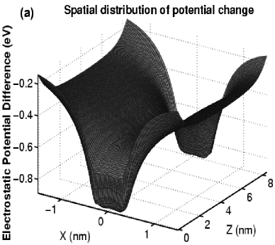
Leónard and Tersoff TersoffNT first pointed out correctly that the strength of the interface coupling doesn’t affect the lineup of the SWNT band in regions moving away from the interface, based on the electrostatics of an ideal cylinder and the confined geometry of the metal-nanotube interface. However, the electrostatics of any nanostruture is three-dimensional. For SWNTs the electrostatic potential change induced by the charge transfer varies in directions both along and perperdicular to the SWNT axis ( axis). This is clearly seen in Fig. 3(a), where we show a cross sectional view of the electrostatic potential change in the plane. For the SWNT with a diameter of , the change in the electrostatic potential inside such narrow cylinder is small, but decays to about of its value at the cylindrical center away from the SWNT surface.
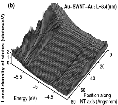
The confined cylindrical geometry and three-dimensional electrostatics of the metal-SWNT interface lead to a completely different physical picture of the band shift from that of the planar metal-semiconductor interface. In particular, the shift of the SWNT band edge in the direction along the SWNT axis doesn’t follow the change in the electrostatic potential. This is illustrated in the local density of states (LDOS) of the Au-SWNT-Au junction as a function of position along the SWNT axis in Fig. 3(b). Note that despite a change of electrostatic potential within of the interface, both the conduction band and valence band edges are nearly contant along the NT axis. LDOS From the LDOS in the middle of the channel, we can determine that for both the Au-SWNT-Au and Pd-SWNT-Pd junction the Fermi-level is located slightly below (by ) the midgap, while for Ti-SWNT-Ti junction it is located above (by ) the midgap. For the case of Au and Ti electrodes, these values are essentially identical to those obtained in the end contact scheme. XueNT
The physical principles of Schottky barrier formation at the metal-SWNT interface can be understood as follows: Since the electrochemical potential (Fermi-level) and therefore the electron occupation in the junction are determined by the electrodes in contact with the SWNT, Datta the band lineup inside the SWNT channel is determined by the self-consistent charge transfer effect through the entire metal-SWNT-metal junction. Therefore, the metal Fermi-level position should be close to the middle of the gap since otherwise extensive charge transfer will occur inside the SWNT channel. Since the screening of the work function difference inside the SWNT junction is weak, the metal Fermi-level should be below (above) the middle of the gap for a high (low) workfunction metal so that the net decrease (increase) of electrons inside the channel shifts the SWNT band edge down (up) relative to the metal Fermi-level. Exactly how this is achieved from the interface to the middle of the channel will depend on the details of the contact without affecting the lineup scheme in the bulk region.
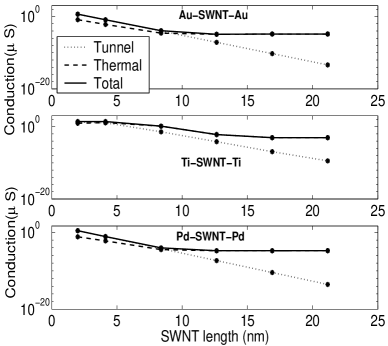
Given the potential shift across the metal-SWNT interface, we can evaluate the length and temperature dependence of the SWNT junction conductance using the Landauer formula and . XueMol ; Datta Here we have separated the conductance into tunneling contribution and thermal-activation contribution . The result at room temperature is shown in Fig. 4. The tunneling conductance for all three junctions decreases exponentially with the SWNT channel length for channel lengths longer than . A separation of contact and bulk effect on the tunneling resistance can thus be achieved using , where is the contact resistance and is the inverse tunneling decay length. We find and for the Au-SWNT-Au, Ti-SWNT-Ti and Pd-SWNT-Pd junctions respectively. Note that the contact resistance is different for the Au and Pd electrodes due to the different interface coupling, but the inverse decay length (a bulk-related parameter) is the same. The room-temperature conductance saturates with increasing SWNT length, because tunneling is exponentially suppressed and transport becomes dominated by thermal-activation over the top of the potential barrier, whose height is approximately independent of the SWNT channel length. For Ti-SWNT-Ti junction, this leads to a transition from tunneling to thermally-activated transport at roughly . For Au/Pd-SWNT-Au/Pd junctions, this transition occurs at channel length of roughly . Consequently we can say that transport through the SWNT junction is bulk-limited at low temperature, but is contact-limited at room temperature.
In conclusion, we have presented an atomistic real-space analysis of Schottky barrier formation at metal-SWNT interfaces with embedded contact. Further analysis is needed that treat both the gate and source/drain field self-consistently within the SWNT junction, to achieve a thorough understanding of nanotube-based devices.
This work was supported by the DARPA Moletronics program, the NASA URETI program and the NSF Nanotechnology Initiative.
References
- (1) Corresponding author. Email: ayxue@chem.nwu.edu
- (2) E.H. Rhoderick and R.H. Williams, Metal-Semiconductor Contacts, 2nd edition (Clarendon Press, Oxford, 1988).
- (3) C. Dekker, Phys. Today 52(5), 22 (1999).
- (4) S.J. Tans, A.R.M. Vershueren, and C. Dekker, Nature 393, 49 (1998); Y. Yaish, J.-Y. Park, S. Rosenblastt, V. Sazonova, M. Brink, and P.L. McEuen, cond-mat/0305108.
- (5) S. Heinze, J. Tersoff, R. Martel, V. Derycke, J. Appenzeller, and Ph. Avouris, Phys. Rev. Lett. 89, 106801 (2002); S.J. Wind, J. Appenzeller, and Ph. Avouris, ibid. 91, 58301 (2003).
- (6) Y. Xue and S. Datta, Phys. Rev. Lett. 83, 4844 (1999).
- (7) F. Leónard and J. Tersoff, Phys. Rev. Lett. 83, 5174 (1999); 84, 4693 (2000).
- (8) A.A. Odintsov, Phys. Rev. Lett. 85, 150 (2000); T. Nakanishi, A. Bachtold and C. Dekker, Phys. Rev. B 66, 73307 (2002).
- (9) T. Ando, T. Nakanishi, and R. Saito, J. Phys. Soc. Jpn. 67, 1704 (1997).
- (10) Z. Yao, C.L. Kane, and C. Dekker, Phys. Rev. Lett. 84, 2941 (2000); J.-Y. Park, S. Rosenblatt, Y. Yaish, V.Sazonova, H. Ustunel, S. Braig, T. A. Arias, P. Brouwer and P.L. McEuen, cond-mat/0305108.
- (11) A. Javey, J. Guo, M. Paulsson, Q. Wang, D. Mann, M. Lundstrom and H. Dai, cond-mat/0309242.
- (12) A. Javey, J. Guo, Q. Wang, M. Lundstrom, and H. Dai, Nature 424, 654 (2003); J. Tersoff, ibid. 424, 622 (2003).
- (13) CRC Handbook of Chemistry and Physics (CRC Press, Boca Raton, 1994).
- (14) Y. Xue, S. Datta, and M. A. Ratner, J. Chem. Phys. 115, 4292 (2001); Chem. Phys. 281, 151 (2002); Y. Xue and M.A. Ratner, Phys. Rev. B 68, 115406 (2003).
- (15) Y. Xue and M.A. Ratner, Appl. Phys. Lett. 83, 2429 (2003); to be published.
- (16) R. Hoffmann, Rev. Mod. Phys. 60, 601 (1988).
- (17) A. Rochefort, D.R. Salahub and Ph. Avouris, J. Phys. Chem. B 103, 641 (1999).
- (18) D. A. Papaconstantopoulos, Handbook of the Band Structure of Elemental Solids (Plenum Press, New York, 1986).
- (19) We assume the embedded parts of the SWNT are surrounded entirely by the metals with overall cylindrical symmetry around the SWNT axis. The SWNT-metal interaction arises from one discrete cylindrical shell of metal atoms, surrounded by the bulk metal and treated using the Green’s function method as detailed in Ref. XueMol, . We use a SWNT-metal surface distance of , close to the average inter-atomic spacings in the SWNTs and metals.
- (20) M. Elstner, D. Porezag, G. Jungnickel, J. Elsner, M. Haugk, Th. Frauenheim, S. Suhai and G. Seifert, Phys. Rev. B 58, 7260 (1998).
- (21) This can be understood as follows: Although the charge transfer-induced electrostatic potential change varies about within of the interface, this variation is much weaker than the atomic-scale electrostatic potential variations within the bare SWNT. Its effect on the LDOS is therefore similar to that of small molecules in the molecular tunnel junction, where detailed studies in Ref. XueMol, have shown the LDOS doesn’t change much with position despite a change in electrostatic potential within in the molecular junction.
- (22) S. Datta, Electron Transport in Mesoscopic Systems (Cambridge University Press, Cambridge, 1995).