Current Induced Excitations in Cu/Co/Cu Single Ferromagnetic Layer Nanopillars
Abstract
Current-induced magnetic excitations in Cu/Co/Cu single layer nanopillars (50 nm in diameter) have been studied experimentally as a function of Co layer thickness at low temperatures for large applied fields perpendicular to the layers. For asymmetric junctions current induced excitations are observed at high current densities for only one polarity of the current and are absent at the same current densities in symmetric junctions. These observations confirm recent predictions of spin-transfer torque induced spin wave excitations in single layer junctions with a strong asymmetry in the spin accumulation in the leads.
pacs:
75.60.Jk, 75.30.Ds, 75.75.+ayear number number identifier
Angular momentum transfer studies in magnetic nanostructures have made tremendous progress during the last few years. Recently, both spin current induced magnetization reversal [1, 2, 3] and spin current driven magnetization precession [4, 5] have been directly observed in magnetic nanostructures. These experiments confirmed seminal predictions by Berger [6] and Slonczewski [7], that a magnet acting as a spin-filter on a traversing current can experience a net torque: (spin-) angular momentum which is filtered out of the current must be absorbed by the ferromagnet. In the presence of a significant angular momentum component transverse to the magnetization of the ferromagnet this leads to a so called spin-transfer torque. A transverse spin-polarization of the electric current was thought to be necessary for current induced excitations of the magnetization. Hence most of the experimental and theoretical work on spin-transfer torque concentrated on spin valve type structures of ferromagnet/normal metal/ferromagnet layers, in which the layer magnetizations may be non-collinear. Only recently, the necessity of a transverse component of spin polarized current has been relaxed [8, 9]. At high enough current densities Polianski et al. [8] and Stiles et al. [9] predict spin wave excitations in thin ferromagnetic layers even when the current is unpolarized.
Polianski et al. [8] have reemphasized the spin-filtering property of a ferromagnet (FM) as the fundamental cause for spin transfer torque. Spin-filtering is present also in normal metal/ferromagnetic metal/ normal metal (NM/FM/NM) pillar junctions with only a single FM layer. In the current perpendicular to the plane geometry a current bias results in spin accumulation on either side of the FM. Fluctuations in the magnetization direction combined with spin diffusion parallel to the NM/FM interfaces result in a spin-transfer torque. At each interface these torques act to align the magnetization along the direction of the spin accumulation. In a perfectly symmetric single layer structure the resulting torques are of equal magnitude but opposite direction and cancel each other. However, if the mirror symmetry is broken the torques acting on each NM/FM interface have different magnitudes. For this case, Ref. [8, 9] predict that an unpolarized current can induce spin wave instabilities and generate spin-wave excitations with wavevectors in the film plane. Instabilities occur when the current bias is such that the direction of the larger spin accumulation is anti-parallel to the direction of the magnetization of the FM. Polianski et al. [8] studied the case of an thin FM with the magnetization being fixed along the current flow direction. Here, the break in symmetry requires asymmetric contacts. Stiles et al. [9] relaxed this requirement and allowed the magnetization to vary along the current flow direction, which also breaks the mirror symmetry. In either case in ideal asymmetric junctions current induced excitations are predicted to occur for only one current polarity and are expected to be absent in perfectly symmetric structures. Both groups made predictions on how single layer instabilities depend on parameters such as the current bias polarity, the FM layer thickness, the degree of asymmetry of the single layer junction and the applied field.
In this letter we report systematic studies of current induced excitations of the magnetization in both symmetric and asymmetric nanopillar junctions containing only a single FM layer. Measurements were performed in high magnetic fields () in the field perpendicular to the plane geometry at 4.2 K. For sufficiently large current densities we observe anomalies in for only one current polarity. Current induced single layer excitations occur only in asymmetric pillar devices (PD) and lead to a decrease of the junction resistance. They are absent in symmetric PDs. Our results confirm the recent prediction of current induced excitations in asymmetric PDs.
Pillar junctions 50 nm in size have been fabricated by means of a nano-stencil mask process [10], which has been used earlier for spin-transfer torque studies in Co/Cu/Co trilayer spin valves [11, 3]. To study the thickness dependence of single layer excitations we combined the nano-stencil mask process with an in-situ wedge growth mechanism. With this approach we have fabricated PDs with a single Co layer of continuously varied thickness across a single wafer [12]. As shown in Fig. 1, structures fabricated by means of an undercut template are intrinsically asymmetric due to the requirement of an inert bottom electrode surface, usually Pt, on top of which the pillar structure is grown. Here, asymmetry refers to the spin-accumulation pattern generated within the PD with respect to the Co layer position. The strong asymmetry due to the choice of Pt as bottom electrode is removed by inserting a second Pt layer. Therefore, the study of spin-transfer in symmetric single layer structures requires the “capping” of the pillar with a Pt layer as indicated in Fig. 1. Many junctions with a FM layer thickness varying from 2 nm to 17 nm and lateral dimensions from 30 nm 60 nm up to 70 nm 140 nm have been studied as a function of bias current and applied field. The range of Co layer thickness covers both the case where the thickness is smaller than the exchange length of Co and the case where the thickness is comparable to the latter (). All junctions in this thickness range exhibit single layer excitations. Here we discuss representative data obtained on PDs with 8 nm and 17 nm and lateral dimensions of 30 nm 60 nm and 50 nm 50 nm respectively. To confirm that the excitations are caused by asymmetric contacts we have repeated experiments with symmetric PDs with a stack sequence of PtRh15 nmCu10 nmCo10 nmCu10 nmPt 15nm.
All measurements reported here were conducted at 4.2 K in a four point-geometry configuration in fields applied perpendicular to the thin film planes. The differential resistance dV/dI was measured by lock-in technique with a 100 A modulation current at Hz added to a dc bias current. As shown in Fig. 1 positive current is defined such that the electrons flow from the bottom electrode of the junction to the top electrode.
A typical magnetoresistance (MR) measurement of a single layer junction at 0 dc bias is shown in Fig. 1.

The resistance has its minimum when the magnetization lies in the thin film plane, i.e. when is orthogonal to . We observe a gradual increase in as we increase the applied field which tilts the magnetization vector out of the thin film plane. Once the applied field exceeds , is collinear with and the resistance saturates at its maximum. From this we conclude that the observed MR is sensitive enough to register (field induced) changes of relative orientation of and . This provides a convenient tool for detecting also current induced changes of the magnetization. It is important to note, that for even the thickest layer we observe a decrease of the resistance in the field sweeps when and start deviating from collinear alignment.
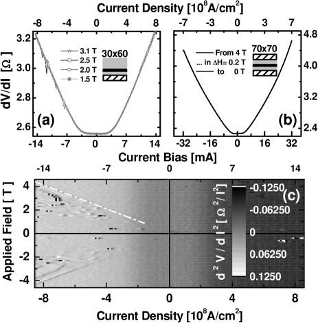
A typical I(V) curve for an asymmetric single layer PD is shown in Fig. 2(a). Here versus is plotted for fields T, 2 T, 2.5 T and T for a 30 nm 60 nm junction with nm. At fields above the demagnetization field ( T) we observe anomalies in the form of small dips at negative current polarity only. The presence of many modes makes it difficult not only to distinguish individual modes but also to find the threshold current for single layer excitations at a particular field value. Note that in the field perpendicular geometry the onset of these excitations always leads to a (small) decrease in resistance, which is opposite to what has been observed in both point contact experiments [13, 14, 15] and trilayer PDs.
To distinguish these excitations from the parabolic background resistance, we plot , which is sensitive to abrupt features in . Plotted on a greyscale as a function of the applied field and the current bias it represents a phase diagram for single layer excitations. An example of such a plot is shown in Fig. 2(c). Here the current is swept from -15 mA to +15 mA while the magnetic field is held constant for each current sweep. For subsequent sweeps the field is stepped from -4.6 T to +4.6 T in 100 mT steps. The “current bias-applied field” plane segregates into two regions separated by a straight line, which we associate with the threshold current, the critical current for single layer excitations. For fields excitations only occur for negative current polarities. At negative current bias excitations are absent below the critical current, whereas above the current threshold many modes are excited. shows a linear dependence on the applied field and can be extrapolated approximately to the origin. Dividing by the nominal junction area , we estimate the field dependence of the critical current density with (A/cm2)/T. We obtain a more accurate estimate for by multiplying with the junction resistance , which is equivalent to dividing by an effective junction area: with (A/T).
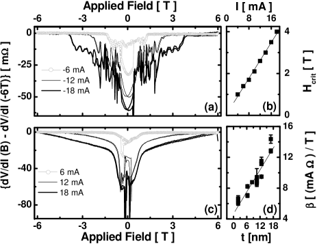
A better way to distinguish the small features of current induced excitations from the varying background resistance is to fix the latter. This can be done by keeping the current constant and sweeping the applied field instead. Here an example of such a measurement is given in Fig 3(a) and (c). Field sweeps at fixed negative current bias are shown in Fig. 3(a), whereas Fig. 3(c) shows the MR at fixed positive currents. The strongest evidence for current induced excitations in single layer junctions comes from the comparison of these two figures. As shown in Fig. 3(c) excitations at fields are absent in the field traces. However, high current densities at positive bias gradually increase the applied field at which the differential resistance saturates.
This effect cannot be attributed solely to the presence of additional (Oersted) fields related to the charge current and is not yet fully understood. There is a dramatic change in the field traces if one applies a negative current bias to the junction. For each fixed current value there is now a critical field , above which the resistance remains constant. However, below the observation of peaks and dips indicates the presence of many (current induced) excitations. is a linear function of the bias current and shifts to higher values as one increases the current. As can be seen in Fig. 3(b), the linear fit of the critical fields can once more be extrapolated to the origin. Hence in both field sweeps at fixed currents and current sweeps at fixed fields one obtains a linear dependence of the critical parameter on the running variable, i.e and . For a particular Co layer thickness the slopes and are equivalent, i.e. . From Fig. 3(b) and the nominal junction area we estimate the current density dependence of with T/(A/cm2). Using the junction resistance as an approximation for the effective junction area we obtain with 73.8 T/(A). Note that for there are large changes in the hysteresis for both current polarities. We attribute these changes to the interaction of the Oersted fields with magnetic domain configurations [12].
We have also studied the thickness dependence of these excitations and summarize the results in Fig. 3(d). For all thicknesses the observed boundary in the “current bias/applied field plane” can be extrapolated close to the origin. Here we only plot the slope of the field dependence of ( as a function of Co layer thickness . We observe an increase of with increasing , (mA)/(T nm). The critical currents increase by approximately a factor of two as one increases the Co layer thickness from 2 nm to 17 nm. Over the same thickness range the junction resistance increase only by % (not shown).
To clarify the origin of these excitations, we have repeated these experiments in symmetric single layer PDs. An example of current sweeps at fixed fields in these structures is shown in Fig. 2(b). Here the current is swept from +32 mA to -32 mA in a 70 nm 70 nm junction. In magnetic fields up to 4 T features such as dips or peaks are absent in the current-voltage characteristics. Also, field sweeps at fixed current do not exhibit any of the strong polarity dependence observed in asymmetric PDs. To summarize, in symmetric junctions current induced excitations are absent up to A/cm2 .
Experimental results and theoretical predictions are in good agreement. Both models give the correct order of magnitude, correct polarity and thickness dependence of in asymmetric structures. Ref. [8] studied the case of uniform magnetization in the current flow direction . Ref. [9] also considered the case where is allowed to vary along . For this case excitations are expected to occur independent of current polarity even in symmetric PDs. However, the predicted critical currents are much larger ( A/cm2) than for the asymmetric case [16]. Once is allowed to vary along , current induced excitations are predicted for both current polarities, albeit, with large differences in the magnitude of critical currents. For example for an asymmetric junction with nm the necessary positive current densities ( A/cm2) far exceed the value which can be sustained by existing PDs. The linear dependence of on can be explained by both models. The (near) zero intercept of is somewhat peculiar but can also be explained if the influence of the shape and finite size of the PD on the spin wave modes is properly accounted for in models [16]. Also the increase of the critical current with increasing Co layer thickness is in agreement with theoretical predictions. An increase of with increasing is expected due to an increase of the (bulk) damping [8, 9]. According to Ref. [9] in thicker films () the variation of along introduces an additional source of asymmetry. This should activate a competing effect which by itself would decrease with increasing . However, to determine which effect would dominate details of layer structure and junction geometry need to be considered. The direct comparison between experimental results and theoretical predictions is further hampered by the change of asymmetry in spin accumulation as we increase the Co layer thickness [17]. For our device geometry and for Co layer thicknesses up to nm ( the dominant source of the current-induced excitations appears to be the asymmetry of the leads.
Finally we would like to address the possibility of current induced excitations in multilayered structures caused by an asymmetry in spin accumulation in the leads. For trilayer structures with a stack sequence of PtCuCo (thin)CuCo (thick)Cu parallel orientation of the magnetization results in a spin accumulation asymmetry at the thick layer similar to the one in single layer junctions discussed above. Hence, high negative currents should lead to spin wave instabilities. Also the anti-parallel configuration leads to a strong asymmetry in spin accumulation at the thicker layer. However, the asymmetry in spin accumulation at the interfaces of the thick layer is now reversed. Therefore, spin wave instabilities are now conceivable for positive current bias. Consequently, a strong asymmetry in spin accumulation should lead to spin wave instabilities in trilayer nanopillars for both current polarities at current densities, similar to those at which magnetization reversal is observed.
In conclusion we have studied current induced spin wave excitations in symmetric and asymmetric pillar junctions with only a single ferromagnetic layer. We have confirmed that excitations occur in asymmetric junctions and are absent in symmetric junctions at similar current densities. We have also shown that in asymmetric junctions the critical currents increase with Co layer thickness. Finally, we have discussed implications of an asymmetry in longitudinal spin accumulation in Co/Cu/Co trilayers.
Acknowledgements.
This research is supported by grants from NSF-FRG-DMS-0201439 and by ONR N0014-02-1-0995.References
- [1] J. A. Katine et al., Phys. Rev. Lett. 84, 3149 (2000).
- [2] J. Grollier et al., Appl. Phys. Lett. 78, 3663, (2001).
- [3] B. Özyilmaz et al., Phys. Rev. Lett. 91, 067203 (2003).
- [4] S. I. Kiselev et al., Nature 425, 380 (2003).
- [5] W. H. Rippard et al., Phys. Rev. Lett. 92, 027201, (2003).
- [6] L. Berger, Phys. Rev. B 54, 9353 (1996).
- [7] J. Slonczewski, J. Magn. Magn. Mater. 159, L1(1996).
- [8] M. L. Polianski, P. W. Brouwer, Phys. Rev. Lett. 92, 26602 (2004).
- [9] M. D. Stiles, Jiang Xiao, A. Zangwill, Phys. Rev. B 69, 054408 (2004).
- [10] J. Z. Sun et al., Appl. Phys. Lett. 81, 2202, (2002).
- [11] J. Z. Sun et al., J. Appl. Phys. 93, 6859 (2003).
- [12] B.Özyilmaz et al., to be published.
- [13] E. B. Myers et al, Science 285, 867 (1999).
- [14] Y. Ji, C. L. Chien, and M. D. Stiles, Phys. Rev. Lett. 90, 106601 2003.
- [15] In Ref. [14] the authors conclude that at high current densities the single layer point contact experiments closely mimic trilayer junctions in which excitations are caused by a spin polarized current and detected via a GMR type of effect. Here the extended film acts as a reference. Hence, excitations lead to a resistance increase and show up as peaks in .
- [16] M. D. Stiles, private communications.
- [17] The total height of the PD is fixed. Therefore, an increase of the Co layer thickness reduces the asymmetry in spin accumulation and hence could increase the critical currents.