Asymmetric - characteristics and magnetoresistance in magnetic point contacts
Abstract
We present a theoretical study of the transport properties of magnetic point contacts under bias. Our calculations are based on the Keldish’s non-equilibrium Green’s function formalism combined with a self-consistent empirical tight-binding Hamiltonian, which describes both strong ferromagnetism and charging effects. We demonstrate that large magnetoresistance solely due to electronic effects can be found when a sharp domain wall forms inside a magnetic atomic-scale point contact. Moreover we show that the symmetry of the - characteristic depends on the position of the domain wall in the constriction. In particular diode-like curves can arise when the domain wall is placed off-center within the point contact, although the whole structure does not present any structural asymmetry.
pacs:
75.47.Jn, 72.10.Bg, 73.63.-bI Introduction
The study of electronic devices at the nanoscale is of paramount importance both from the scientific and the technological point of view. One important aspect is related to spin polarized electronic transport in magnetic materials, a field usually known as spintronics Prinz . This has been subject of intense study in recent years, garcia1999 ; garcia2001 ; zchopra since the discovery of the giant magnetoresistance effect (GMR) in magnetic multilayers. baibich_gmr ; binasch_gmr ; pratt_gmr ; gijs_gmr GMR is the drastic change of the electrical resistance of a magnetic multilayer when a magnetic field is applied. The effect of the field is to align ferromagnetically the magnetization vectors of adjacent magnetic layers, which otherwise are oriented antiparallel to each other. The parallel state has a lower resistance than the antiparallel and this produces the magnetoresistance. GMR has already led to the construction of the present generation of magnetic data storage devices. However, in order to reach storage densities of the order of Terabit/in2 a substantial downscaling of the read/write devices is needed. One possible avenue to this target is given by magnetic point contacts (MPC’s), where the lateral size of the typical contacts approaches the atomic scale.
Recent experiments have shown that nanoscaled magnetic point contacts may present huge magnetoresistance garcia1999 ; garcia2001 ; zchopra ; versluijs ; oscar1 ; oscar2 ; oscar3 reaching up a few hundred thousand percent. comment This result alone can be seen as a major leap toward nanoscopic magnetic memory read/write devices. In addition, it is important to report that electro-deposited nickel point contacts present highly asymmetric - characteristics typical of a diode-like behaviour. oscar1 ; oscar2 A complete explanation of both these effects is still lacking.
To date there is a large debate around the origin of the large magnetoresistance effects in MPC’s. On the one hand, it has been argued that magnetic field-induced mechanical effects can produce a large GMR. In fact, either magnetostriction, dipole-dipole interactions between the apexeschung_dipole and magnetically induced stress reliefansermet may have the effect of compressing the nanocontact once a magnetic field is applied. This enlarges the cross section of the MPC and consequently the resistance of the junction decreases. On the other hand, there are also strong indications that mechanical effects alone are not able to account for whole magnetoresistance. Specifically García et. al. have shown that the behaviour of MPC’s does not comply with mechanical changes, in particular with magnetostriction effects. garcia1999 ; garcia2001
One important step toward the understanding of the magnetoresistance effect in point contacts comes from the work of Bruno.bruno He has shown that if the magnetic moments on the apexes of the constriction are not aligned parallel to each other, then a domain wall (DW) will be formed inside the constricted region. The main features of this DW are quite different from those of the well know Bloch bloch ; landau and Néel neel walls. In particular, the crucial point is that the length of the DW is predicted to be as long as the diameter of the constriction. This result suggests that the DW trapped in an atomic scale MPC may be very sharp, only a few atomic planes long. At this length scales a DW produces a rather strong spin-dependent scattering potential and large magneto-induced effects are somehow expected. In this context it is important to report that such an extreme confinement has been already achieved by contacting two magnetic grains with different orientation. zchopra
Since Bruno’s seminal idea a number of theoretical works on transport through magnetic domain walls have been presented. maekawa ; maekawa2000 ; nakamura ; kelly These consider equilibrium transport in the spirit of the Landauer-Büttiker formalism; landauer current induced effects such as charging of the point contact and, quite possibly, movement of the domain wall have not been taken into consideration. However in low dimensional systems such as these even small biases might cause charge accumulation inside the MPC, changing its transport properties.ruitenbeek
In this work we investigate whether the transport properties of MPCs, in particular the magnetoresistance effect and the asymmetry in the - curves, can arise from electronic effects only. We model the magnetoresistance in MPC using the typical spin-valve scheme: we assume that in the absence of a magnetic field, the magnetization vectors of the two leads are aligned opposite to each other (antiparallel state). Therefore in the zero field situation a sharp DW is formed inside the MPC. Then, when a magnetic field is applied, the magnetic moments of the leads align parallel to each other and the wall is eliminated (parallel state). In this configuration the resistance is reduced giving rise to a GMR-like effect. Our task is to calculate the - curves of both the parallel and antiparallel states, assuming a simple but reasonable electronic structure for the material forming the MPC and considering charging effects.
We also investigate the effects of the position of the DW inside the constriction. When the DW is positioned in the centre of the constriction, we expect symmetric - curves, since no asymmetry is present in the MPCs. However, if the position of the wall is shifted from the midpoint, and charging effects are present, we expect the appearance of asymmetric - curves. It is noteworthy to mention that a linear response Landauer-Büttiker approach to transport cannot account for charging effects, and therefore cannot describe asymmetric - characteristics.
This paper is organized as follows. In the next sections we introduce our self-consistent technique based on the non-equilibrium Green’s function formalism keldysh ; datta ; Tsukada ; stokbro with tight-binding Hamiltonians.zhao Then we will use our method to study the effects due to the existence of a domain wall on the electronic transport of MPC’s.
II Non-equilibrium transport method
In order to describe the transport properties of MPC’s, including charging effects, we use the non-equilibrium Green’s function approach based on the Keldysh formalism.keldysh ; datta ; Tsukada ; stokbro We start by dividing an open system into three distinct regions: two semi-infinite electrodes and a central scattering region where the MPC is located. Here the leads act as charge reservoirs, therefore they set the temperature and electronic distribution of the junction in the steady state. In principle calculating the electronic structure of such a system would involve the solution of a quantum mechanical problem for a non-periodic open system, which consist of an infinite number of degrees of freedom. However, there are two reasons that allow us to focus only on the central scattering region. Firstly, we note that most of the potential drop occurs at the nanoconstriction. This observation underpins the assumption that the relevant modification of the electronic structure due to the presence of a bias will occur to those degrees of freedom corresponding to the central region. Secondly we assume that the rearrangement of the electronic structure in the central region does not change the electronic structure of the electrodes. Note that this is a well sustained approximation for good metals where the screening length is very short and the relaxation of the charge density occurs within a few atomic planes. Under this condition their dynamics can be neglected with the exception of a rigid shift of the chemical potential due to the bias. Therefore we reduce our problem to that of calculating the Green’s function of the central scattering region.
Using an orthogonal tight-binding model we construct the retarded Green’s operator of the scattering region in the presence of the leads as followsdatta
| (1) |
where is the Hamiltonian of the scattering region and and are the leads self-energies. These are energy dependent potentials added to the Hamiltonian to account for the interaction with both the left and the right lead. The self-energies are matrices of the same dimension of and of the form
| (2) |
and
| (3) |
where and are the surface Green’s functions for the left and right leads respectively and () is the coupling matrix between the scattering region and the left (right) lead. Note that given by the equation (1) is formally the Green’s function of the effective Hamiltonian for the scattering region in presence of the leads
| (4) |
This Hamiltonian is non-hermitian since the ’s are not hermitian, consequently the number of electrons in the scattering region is not conserved.
One of the crucial aspects of the method is computing the surface Green’s functions . Several ways for calculating the surface Green’s functions of a semi-infinite system are available in the literature, ranging from recursive methods datta to semi-analytical solutions. sanvito In this work we use the technique presented by Sanvito et. al. sanvito that calculates the surface Green’s function exactly. The method first constructs the Green’s function of an infinite system and then derives the surface Green’s functions by introducing the appropriate boundary conditions. Following this procedure a general semi-analytical expression for the surface Green’s function is derived. The benefit of our method is to avoid the typical complications of the recursive methods, preserving information about the individual scattering states in the leads. sanvito
This formulation of the transport problem can account for finite bias. As we discussed previously the bias is assumed not to change the electronic structure of the leads, but only to shift all energy levels. Therefore is introduced as a rigid shift of the leads’ Hamiltonian on-site energies
| (5) |
where is the identity matrix. This in turn redefines the leads self-energies in the following way
| (6) |
In contrast to the leads, due to the presence of a large potential drop, the effects of a finite bias on the scattering region need to be calculated self consistently. This is done by noting that is a function of the scattering region single particle charge density onlykohn . This property gives us a clear prescription for performing a self-consistent calculation.
We first compute the scattering region Green’s function (equation (1)) for , where the Hamiltonian is evaluated at a given initial charge density . Then from the Green’s function we calculate the new charge density , which is then used to construct the new Hamiltonian . This procedure is iterated until reaching self-consistency, that is when . Note that a fundamental requirement is that the final self-consistent density matrix matches exactly that of the leads at the boundaries. Therefore we usually enlarge the scattering region to contain a few atomic planes of the leads (those where the electronic structure is different from that of the bulk). The exact number of such planes depends on the screening length of the material considered. As a general rule we add as many planes as necessary for the charge density of the more external plane to match exactly that of the infinite leads. In this case the description of the leads in terms of self-energies is perfectly justified.
Within this scheme the density operator of the scattering region is evaluated from the Green’s function
| (7) |
where
| (8) |
and is the Fermi distribution function calculated at the chemical potentials of the leads .
In general it can be very clumsy to solve the equation (7) numerically, since the integration has to be performed over the entire real axis. However, we can both add and subtract the term to the equation (7) rewriting the density operator as
| (9) |
where now
| (10) |
| (11) |
We can interpret as the density matrix at equilibrium, i.e. the one calculated when both the reservoirs have the same chemical potential , and as the out of equilibrium charge density obtained when a potential bias is applied across the device. The separation of into and has some important numerical advantages. Firstly is bounded by the difference between the Fermi functions and therefore one needs to perform the integration only in the energy range between the two chemical potentials. Secondly, since the Green’s function is analytical, can be integrated in the complex plane using a standard contour integral technique. lang ; stokbro In this way we have reduced an unbounded integral over the real energy axis to a bounded one over the real axis plus a well behaving unbounded integral in the complex plane. In addition, the lower limit of the contour integral is set by the lowest between the bottom of the conduction band of the leads and the deepest of the energy levels of the scattering region.
Once self-consistency has been achieved and both the charge density and the potential have been calculated, we can finally evaluate the current through the device
| (12) |
The term is the energy-dependent total transmission probability datta Note that the total current is nothing but times the energy-dependent total transmission coefficient integrated over the bias window. This latter depends not only on the electron energy but also over the bias applied , since the potential across the device is bias-dependent. However, this does not mean that the electrons exchange energy while passing through the device. On the contrary the transport is still phase-coherent. The current is carried by electrons crossing the device with probability , leaving an occupied state of the lead with the higher chemical potential and filling an empty state at the same energy in the other lead. At low bias () and temperature (), the equation (12) reduces to the well-known linear response Landauer-Büttiker formula.datta
III The Model
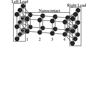
The theoretical approach to transport described in the previous section is general and can be applied to a number of different systems and model Hamiltonians. Figure 1 shows a sketch of the point contact used in the present calculations. Our structure consists of two semi-infinite rods representing the leads connected through a constricted region containing four atomic planes with a square four-atom cross section. This models a nickel nanowire connected to two current/voltage electrodes. Each atomic site is described by a spin-dependent two-orbital tight-binding model. One orbital forms a broad band and represents the orbitals while the other forms a narrow band and represents the orbitals. Spin degeneracy is lifted on the states by adding a spin-dependent contribution to the on-site energy. The spin on-site energy for the -th orbital at each site ( labels both the position and the orbital , ) is given by
| (13) |
The first term, is the spin independent band centre. The second term, which is not zero only for the orbitals is a Stoner-like term with the exchange integral, and the magnetic moment at each site. This latter is given by the difference in the orbital occupation between majority and minority spins. Finally, the last term is introduced to ensure charge neutrality. vega It is proportional to the difference between the self-consistent atomic charge density and that at equilibrium . is calculated self-consistently from the non-equilibrium density matrix (equation (9)). The total number of electrons and the orbital occupation are respectively given by
| (14) |
and
| (15) |
where is the projector over the state . Finally here we consider only first nearest neighbour coupling with elements , and an hybridization term .
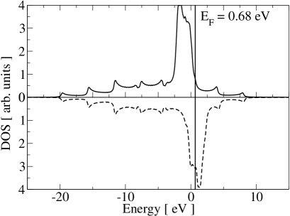
Before turning our attention to the non-equilibrium problem, we must set the parameters of the calculation, i. e. we must determine some reasonable values for , , and . In particular, the leads depicted in figure 1 should describe the bulk properties of a strong ferromagnet (a ferromagnet where the majority spin band is completely occupied). To this purpose we performed self-consistent calculations of the electronic structure of a 33 infinite rod (representing the leads). We assume an atomic occupation of three electrons per atom (two electrons in the orbitals and one electron in the orbital), and we fix and in order to reproduce the correct bandwidth of the and band of Ni respectively. me2 Then we set , and to give respectively the Stoner instability, the charge transfer from the to the band, and the local charge neutrality. A good description of a strong ferromagnet is given by the following choice of parameters: eV, eV, eV, eV, eV, eV and eV. Figure 2 shows the DOS resulting from our calculations, where one can clearly see a completely filled band for majority spin and an half-filled band for the minority.
We are now ready to calculate the - curve of the nanocontact. In our calculations, we considered two possible configurations depending on whether the magnetizations in each of the leads are aligned parallel or anti-parallel with respect to each other. In the latter case, a domain wall will appear in the middle of the constriction with characteristic length scales comparable to the length of the nanowire. In addition, we study the effect of the position of the DW on the - characteristics of the MPC. In all cases presented here we consider collinear spins. This is justified by a recent calculation from Imamura et. al. maekawa who have used a Heisenberg model in a mean field approximation to show that, in the case of a domain wall pinned in a constriction, there is no spin precession and minority and majority bands can be treated separately.
IV Results and Discussion
As mentioned previously we model a point contact following the sketch of figure 1, where we consider a simple cubic lattice of nickel atoms with the MPC composed by a two-atom-wide four-atom-long chain connected to two semi-infinite rods representing the current/voltage electrodes.
We start by considering the situation where no magnetic field is applied to the MPC. In this case we assume that a DW forms inside the constriction. However it is worth noting that the position of the DW is not a priori determined, since in general it is given by pinning centers in the junction. These are not present in our calculations and therefore we have considered two possibilities: 1) the DW is situated half way across the device (symmetrical case), and 2) the DW is situated between the third and fourth transversal plane (asymmetrical case). It important to stress that in both the situations the domain wall is abrupt and that the direction of the magnetization changes by 180o across the Bloch wall.
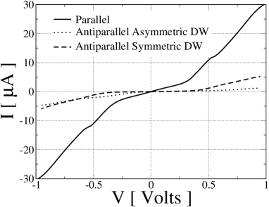
Figure 3 shows our results for all these cases. As a matter of notation, in all the - curves presented hereafter we define positive bias when the current flows from the left hand-side to the right hand-side (from plane one to four) and we use the left-hand side lead to set the spin direction. In figure 3 the dashed curve shows our result for a symmetric DW and the dotted line the asymmetric. We can clearly see that an asymmetric - curve appears when the domain wall is asymmetrically placed with respect to the junction.
Before discussing the reason for this asymmetry we consider the case when a magnetic field strong enough to align the magnetic moment of the leads is applied. We simulate this situation by setting the magnetization of the leads to be parallel to each other. The self consistent solution now does not present any Bloch wall and the corresponding - characteristic is also shown in figure 3 (solid line). From the picture it is clear that the current for the parallel configuration is larger than that of both the antiparallel ones at any bias. This of course means that the point contact presents positive magnetoresistance at any bias. It is also worth noting that such a magnetoresistance increases as the bias increases, in particular for the case in which the DW is asymmetrically placed in the junction. This suggests that a large GMR entirely due to the electronic properties of the point contact can be obtained, although for a fully quantitative estimation a more realistic description of the electronic structure and the structural conformation of the point contact is needed.
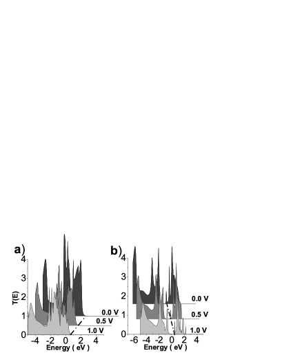
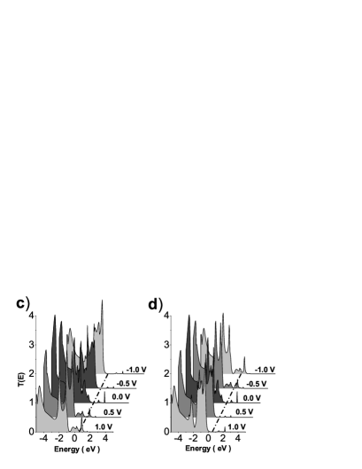
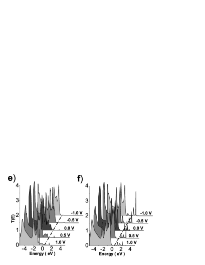
Let us now turn our attention to the asymmetry properties of the - curves. In order to achieve a qualitative understanding of the underling physics it is useful to calculate the transmission coefficients as a function of the energy for different biases and for the three situations studied (parallel, antiparallel symmetry and antiparallel asymmetric). These are presented in figure 4.
Since the current is essentially given by the energy integral of the transmission coefficient over the bias window (see the equation (12)), from the picture one can establish the relative contribution of the different spin currents to the total current for a given bias. For the parallel case (figure 4a and 4b) the current has contributions from both the spin directions, although the majority spins contribute to the transmission coefficient below the Fermi level and the minority contribute above. Borrowing the notation from molecular transport theory datta we can say that the majority spin conductance is through the highest occupied molecular orbital (HOMO), while the minority is through the lowest unoccupied molecular orbital (LUMO).
The situation changes drastically when we look at the antiparallel alignment. Consider first the symmetric DW case. From the figures 4c and 4d one can see that the conductance around is dominated by majority spins for positive bias and by minority spins for negative bias. We can understand this behaviour by looking at the cartoon of figure 5.
Here we schematically model our magnetic point contact as a magnetic molecule. When the magnetization of the two leads are aligned parallel to each other (and to the molecule) the molecule presents a majority spin HOMO and a minority spin LUMO state (figure 5a). Both these states extend through the whole molecule and can give rise to resonant transport.

In contrast, in the antiparallel case the DW formed inside the molecule splits the HOMO and LUMO states. In fact, since the transmission through the DW is small and the coupling with the leads strong, we can now model our system as two molecules strongly attached respectively to the left and the right lead, but weakly coupled to each other. This gives rise to the level scheme presented in figure 5b, which is strictly valid only in the case the DW resistance is infinite. Within this scheme the left hand-side part of the PC couples strongly with the left lead therefore presenting a majority spin HOMO and a minority spin LUMO. The situation is opposite on the right hand-side since the magnetization of the right lead is rotated. Recalling the fact that we do not consider the possibility of spin mixing, this configuration presents a large resistance since there are no resonant states with the same spin extending through the entire point contact. If we now apply a bias there will be level shifting. This aligns the majority spins HOMO on the left with the LUMO on the right for positive bias (figure 5c) and the minority LUMO on the left with the HOMO on the right for negative bias (figure 5d). Therefore this mechanism leads to majority spin conductance for positive bias and minority spin conductance for negative.
From this simple scheme it is also easy to explain the symmetry properties of the - curves. These are mainly given by the charging properties of the whole structure. For positive bias and symmetric DW charge is accumulated in the first two atomics planes to the left of the DW and it is depleted in the two atomic planes to the right. This is demonstrated in figure 6 where we present the net charge on each atomic plane as a function of bias voltage. According to the equation (13) charge accumulation (depletion) moves the molecular levels toward higher (lower) energies. In the case of a symmetric DW the molecular states to the left and to the right of the Bloch wall charge in a symmetric way with respect to the bias direction. This means that the level alignment responsible for the large current will occur for the same bias difference independently from the bias polarity.

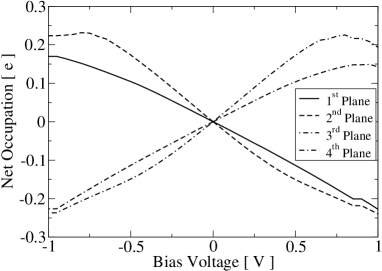
In contrast, when the DW is between the third and the fourth plane, more charge can be accumulated (depleted) to the left of the DW with respect to the right (see figure 7), since more states (atomic planes) are available. In other words the energy levels do not shift at the same rate for positive and negative bias. This means that the alignment of the energy level now depends on the bias polarity, leading to an asymmetric - curve. Note that the mechanism for asymmetry proposed here does not require different coupling between the point contact and the two leads, but only a non-symmetric position of the DW within the point contact.
In summary, we have calculated the - curve for a model magnetic point contact, and demonstrated that large magnetoresistance can be obtained solely from its electronic properties. This is the result of strong scattering through a domain wall pinned inside the contact. We have also investigated the rôle of the position of the DW inside the junction and its effect on the - curves. Our main result is that largely asymmetric - curves can be found when the DW is asymmetrically placed inside the point contact, although the whole structure does not present any structural asymmetry. We have interpreted this result in terms of the charging properties of the junction and of spin-dependent HOMO/LUMO alignment. Although our results are semi-quantitative and a more accurate description of the electronic structure of the materials forming the point contact is needed, we believe that large asymmetry of the - curve and GMR are a common feature of atomic scale magnetic point contacts.
Acknowledgments
This work is sponsored by Science Foundation of Ireland under the grant SFI02/IN1/I175. A.R.R. thanks Enterprise Ireland for financial support (grant EI-SC/2002/10). We acknowledge useful discussions with J.M.D. Coey and O. Céspedes Boldoba.
References
- (1) G. Prinz, Science 282, 1660 (1998); G. Prinz, Phys. Today 48, 58 (1995)
- (2) N. García, M. Muñoz, and Y. W. Zhao, Phys. Rev. Lett. 82, 2923 (1999).
- (3) N. Gracía, M. Muñoz, G. G. Qian, H. Rohrer, I. G. Saveliev, and Y. W. Zhao, Appl. Phys. Lett. 79, 4550 (2001).
- (4) S. Z. Hua and H. D. Chopra, Phys. Rev. B, Rapid Communications 67, 060401 (2003).
- (5) M. N. Baibich, J. M. Broto, A. Fert, F. N. V. Dau, F. Petroff, P. Etienne, G. Creuzet, A. Friederich, and J. Chazelas, Phys. Rev. Lett. 61, 2472 (1988).
- (6) G. Binasch, P. Grünberg, F. Saurenbach, and W. Zinn, Phys. Rev. B 39, 4828 (1989).
- (7) W. P. Pratt Jr., S. F. Lee, M. S. J, R. Loloee, P. A. Schroeder, and J. Bass, Phys. Rev. Lett. 60, 3060 (1991).
- (8) M. A. M. Gijs, S. K. J. Lenczowski, and J. B. Giesbers, Phys. Rev. Lett. 70, 3343 (1993).
- (9) J. J. Versluijs, M. A. Bari, and J. M. D. Coey, Phys. Rev. Lett. 87, 26601 (2001).
- (10) O. Cespedes, M. A. Bari, C. Dennis, J. Versluijs, G. Jan, J. O’Sullivan, J. F. Gregg, and J. M. D. Coey, J. Magn. Mat. 492, 242 (2002).
- (11) O. Cespedes, M. A. Bari, C. Dennis, J. Versluijs, G. Jan, J. O’Sullivan, J. F. Gregg, and J. M. D. Coey, in J. App. Phys. (MMM02, 2003), to be published.
- (12) O.Céspedes, A. R. Rocha, S. Lioret, M. Viret, C. Dennis, J. Gregg, S. van Dijken, S. Sanvito, and J. Coey, in J. Mag. Mag. Mat. (International Conference on Magnetism, 2003), to be published.
- (13) Throughout the paper we will use the “optimistic” definition of magnetoresistance , where is the magnetic field dependent resistance of the device.
- (14) S. H. Chung, M. Muñoz, N. García, W. Egelhoff, and R. D. Gomez, J. App. Phys. 93, 7939 (2003).
- (15) J. E. Wegrowe, T. Wade, X. Hoffer, L. Gravier, J. M. Bonard, and J. P. Ansermet, Phys. Rev. B 67, 104418 (2003).
- (16) P. Bruno, Phys. Rev. Lett. 83, 2425 (1999).
- (17) F. Bloch, Z. Phys. 74, 295 (1932).
- (18) L. D. Landau and E. M. Lifshitz, Z. Phys. Sowjetunion 8, 153 (1935).
- (19) L. Néel, C. R. Acad. Sci. (Paris) 241, 533 (1955).
- (20) H. Imamura, N. Kobayashi, S. Takahashi, and S. Maekawa, Mat. Sci. Eng. B86, 107 (2001).
- (21) H. Imamura, N. Kobayashi, S. Takahashi, and S. Maekawa, Phys. Rev. Lett. 84, 1003 (2000).
- (22) K. Nakanishi and Y. O. Nakamura, Phys. Rev. B 61, 11278 (2000).
- (23) J. B. A. N. van Hoof, K. M. Schep, A. Brataas, G. E. W. Bauer, and P. J. Kelly, Phys. Rev. B 59, 138 (1999).
- (24) M. Büttiker, Y. Imry, R. Landauer, and S. Pinhas, Phys. Rev. B 31, 6207 (1985).
- (25) S. K. Nielsen, M. Brandbyge, K. Hansen, K. Stokbro, J. M. van Ruitenbeek, and F. Besenbacher, Phys. Rev. Lett. 89, 066804 (2002).
- (26) L. V. Keldysh, Sov. Phys. JETP 20, 1018 (1965).
- (27) S. Datta, Electronic Transport in Mesoscopic Systems (Cambridge University Press, Cambridge, UK, 1995).
- (28) M. B. N. Kobayashi and M. Tsukada, Phys. Rev. B 60, 17064 (1999).
- (29) M. Brandbyge, J.-L. Mozos, P. Ordejón, J. Taylor, and K. Stokbro, Phys. Rev. B 65, 165401 (2002).
- (30) B. Wang, G. Wang, Y. Ren, H. Sun, X. Chen, and J. Zhao, J. of Phys. Cond. Matt. 15, 2327 (2003).
- (31) S. Sanvito, C. J. Lambert, J. H. Jefferson, and A. M. Bratkovsky, Phys. Rev. B 59, 11936 (1999).
- (32) N. D. Ashcroft and N. D. Mermin, Solid State Physics (Int. Thompson Pub., 1976).
- (33) H. Hohenberg and W. Kohn, Phys. Rev. 136, B864 (1964).
- (34) A. R. Williams, P. J. Feilbelman, and N. D. Lang, Phys. Rev. B 26, 5433 (1982).
- (35) R. Robles, J. Izquierdo, and A. Vega, Phys. Rev. B 61, 6848 (2000).
- (36) S. Sanvito, C. J. Lambert, and J. H. Jefferson, Phys. Rev. B 60, 7385 (1999).