Electronic mechanism of ion expulsion
under UV nanosecond laser excitation of silicon:
Experiment and modeling
Abstract
We present experimental and modeling studies of UV nanosecond pulsed laser desorption and ablation of (111) bulk silicon. The results involve a new approach to the analysis of plume formation dynamics under high-energy photon irradiation of the semiconductor surface. Non-thermal, photo-induced desorption has been observed at low laser fluence, well below the melting threshold. Under ablation conditions, the non-thermal ions have also a high concentration. The origin of these ions is discussed on the basis of electronic excitation of Si surface states associated with the Coulomb explosion mechanism. We present a model describing dynamics of silicon target excitation, heating and charge-carrier transport.
pacs:
52.38.Mf, 68.34.Tj, 68.35.Rh, 79.20.DsI Introduction
Laser ablation technique has been widely used for thin film deposition and nanoparticles synthesis. For these applications, understanding of dynamics and mechanisms of particle desorption and ablation from the irradiated surfaces is of crucial importance. For nanosecond laser pulses, it is generally accepted that the ablation mechanism of normal vaporization gives way to phase explosion with increasing laser fluence 1 . At low laser fluences near ablation threshold, electronic mechanism of high-energy ion emission has been proven to play a role in initiating the ablation process, mainly for dielectrics and semiconductors 2 ; 3 . For ultrashort laser pulses, the electronic mechanisms of desorption 4 and ablation 5 ; 6 for both dielectric and semiconductor targets are studied extensively, whereas for nanosecond pulses there is a lack of both the experimental and theoretical analyses.
In this paper, we present the results of the experimental and theoretical studies of ion ejection from the Si targets induced by UV nanosecond laser pulses in a wide range of laser fluences in the regimes from those well below melting threshold up to developed ablation. Non-thermal ions have been detected at very low laser fluence. The theoretical study of ion ejection involves an analytical analysis and numerical modeling of charge transport in the laser-irradiated target. We attribute the high-energy ion emission to the generation of a strong electric field due to the electron photoemission process (the Coulomb explosion mechanism).
II Experimental
Clean (111) Si surface was passivated by hydrogen in a usual chemical way 7 . Ablation was carried out in a high vacuum chamber (pressure Torr) at an incidence angle of 45o using an ArF excimer laser ( eV, 15 ns pulse duration at FWHM). The set of masks was used to select the homogeneous part of the laser beam. The laser spot size on the target and laser fluence ( were 0.5 mm2 and J/cm 2, respectively. The target was rotated/translated during measurements to avoid cratering. The expansion dynamics and origin of the desorbed particles were analyzed by reflectron time-of-flight (TOF) mass spectrometer.
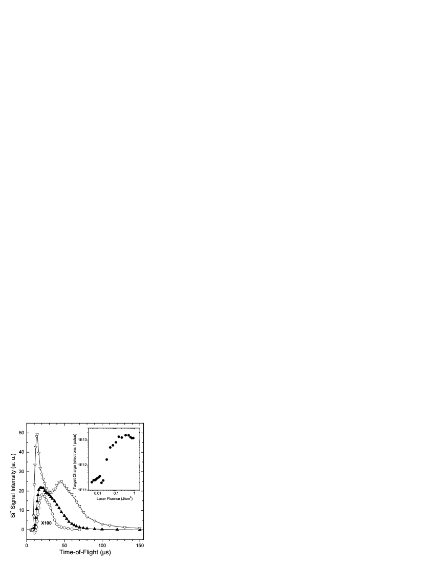
open circles – 0.26 J/cm2 intensity (multiplied by 100);
dark triangles – 0.42 J/cm2;
open triangles – 1.02 J/cm2.
The target - mass spectrometer distance was 126 mm.
Inset shows charge of silicon target versus laser fluence.
The most abundant desorbed species, Si+, are observed already at 0.2 J/cm2, well below melting threshold determined by time-resolved reflectivity measurements to be J/cm2 (see 8 and references therein) that is consistent with the other studies 9 ; 10 . Neutral monatomic Si particles are detected only at J/cm2. Attempts to detect charged or neutral clusters, excepting silicon ions dimmer 11 , have been unsuccessful. Figure 1 shows the typical TOF spectra of Si+ at different fluences. At low laser fluence (0.26 J/cm2on the Fig. 1, the TOF spectrum consists of an only population of Si+ ions. The spatial distribution of this kind of ions is narrow, strongly peaked relatively to the target normal and, up to the melting threshold, the kinetic energy ( eV) is a weak function of laser fluence that is typical for non-thermal desorption/ablation 3 ; 12 .
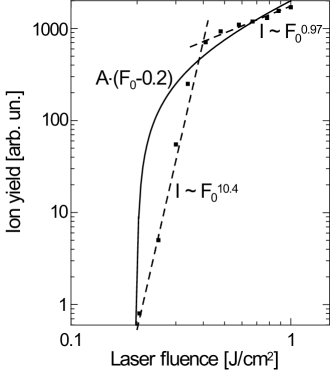
Increasing laser fluence above the melting threshold leads to broadening of Si+ TOF distribution (see Fig. 1, fluence 0.42 J/cm and to formation (from J/cm of a well-pronounced low-energy distribution 13 . The appearance of the low-energy Si+ concurs with the development of Si surface melting. The intensity of this population rapidly increases with fluence and becomes dominant at J/cm2. The abundance of Si+ species versus laser fluence (Fig. 2, experimental points) shows an abrupt change in the behavior of the experimental data that can be treated as the change of the ejection regime. The first regime, corresponding to the generation of the fast population, exhibits a very strong non-linear dependence on fluence, , that is a typical feature of the multi-particle ejection process 3 . The second regime, starting after melting, shows near-linear Si+ abundance variation with fluence.
The expulsion of the non-thermal Si+ ions is attributed to accumulation of a positive charge on the silicon surface as a result of electron photoemission. This charge has been evaluated by measuring a compensating current variation between the Si target and ground 14 during laser pulse. The positive charge is accumulated already at J/cm2 (see inset on Fig. 1), increasing near linearly up to a saturation level of elementary charges per pulse at J/cm2. Exactly at these fluences we detect the first non-thermal ions. Both the target charge saturation and ions ejection clearly indicate that Si surface reaches the critical, threshold, conditions corresponding to dynamical equilibrium between primary particles ejection (photoelectrons) and desorption of the secondary species (positively charged ions).
III Modeling
An assumption for the electron photoemission under the UV laser irradiation, when photon energy exceeds work function, reads as
| (1) |
where , is the laser power of a Gaussian temporal shape:
| (2) |
is laser pulse duration (FWHM), and are the absorption and reflection coefficients, is the electron escape depth, is the distance from the target surface toward the bulk depth, hv is the energy of laser light quantum. The expression (1) implies that the laser-generated electrons whose momentum component normal to and in the direction of the surface are immediately photoemitted from the surface and below surface region with an exponential decreasing within the bulk 5 .
An estimate of the number of electrons photoemitted through a unit surface area ( is obtained by integrating the photoemission term over time and space that gives:
| (3) |
Under the assumption that the target is unearthed and there is no electron supply from the radiation-free sides of the target, the electric field generated on the target surface can be estimated by using the Gauss law (the net positive charge of the target is equal to the charge of the photoemitted electrons):
| (4) |
where is the target width and is dielectric permittivity of bulk silicon.
The threshold electric field necessary to be exceeded in order to break the atomic bonds in crystalline silicon can be estimated through the energy density of the electric field, . The value falls at an atom in the crystal, where is a volume occupied by atom. The binding energy of an atom on the target surface estimated from the latent heat of sublimation, = 16115 J/g 7 , is eV. Thus, the threshold electric field is of order or 2.651010 V/m for crystalline silicon. Laser fluence above which the non-thermal ions can be observed is:
| (5) |
With 10 Å it gives J/cm2 that is in good agreement with the experimental observations. The excess of positive charge in the target for generation of the threshold electric field is or electrons escaped from the irradiation spot size of 0.5 mm2 that is in excellent agreement with the measured electric residue.
A strongly charged target tends to take off the electrostatic stress, decreasing the electric field below its threshold value through ion expulsion. The number of ions thrown out from the target by the electrostatic force can be evaluated as
| (6) |
or 1.410 for our irradiation conditions (laser fluence is taken in J/cm. This dependence follows the general tendency observed experimentally (Fig. 2, solid line). Thus, a seeming change in the ablation regime from the strong non-linear to near-linear dependence of ion yield vs. laser fluence can be roughly described by a shifted linear dependence [Eq. (6)].
More sophisticated description can be reached by modeling the electron dynamics in the laser-irradiated semiconductor targets. Here we shall consider only the target charging effect without concerning the ion ejection process, both electrostatic and thermal. Our model is based on the continuity equations for electron and hole generation, including one-photon ionization, Auger recombination and the photoemission process according to Eq. (1), and we incorporate the electric current written in the drift-diffusion approach into the equations:
| (7) |
| (8) |
Here are the density, mobility and the diffusion and Auger recombination coefficients, respectively; indices and refer to the electrons and holes. The diffusion coefficients are calculated as and with the carrier temperature . The photoemission and diffusion lead to charge separation in the target that results in the electric field generation described by the Poisson equation with the boundary condition according to the Gauss law. The energy equations for the electron and lattice subsystems 15 degenerate into an only equation at fairly long laser pulses of ns time scale 16 ; 17
| (9) |
The vaporization rate is defined under the assumption that the flow of vaporized material from the surface follows the Hertz-Knudsen equation and the vapor pressure above the vaporized surface can be estimated with the Clausius-Clapeyron equation:
| (10) |
Thermodynamic and optical properties of silicon (specific heat , thermal conductivity , latent heat of vaporization , boiling temperature , absorption coefficient , and reflection coefficient ) were taken from Ref. 9 . The initial and boundary conditions are
| (11) |
with being the initial temperature uniform across the target. The target was divided into an irregular grid, dense in the absorption region (cells of 5 Å) and rarefying toward the target depth. We used an explicit scheme for solving the described system of equations. The time step was selected empirically to satisfy the numerical scheme stability and the approximation of the original equations.
IV Results and discussion

The modeling results are presented in Figs. 3, 4. To the end of the laser pulse, the surface charge reaches almost 60%, an unexpected value for silicon irradiated by low laser fluence. The densities of the electrons and holes are presented in Fig. 3. Considerable charging takes place in a surface zone of order of 2 nm wide ( atomic monolayers). It is generally agreed that, because of efficient Auger recombination, a silicon target can not be ionized to a high ionization degree at moderate laser fluences. That is a major argument against the Coulomb explosion mechanism. Our modeling shows that a thin surface layer of the target reaches a high ionization degree, but therewith this layer occurs to be strongly depleted of electrons. Extremely high density of positive charge is gained in a few monolayers, implying the strong repulsion force between the ions. First of all, adatoms, which have lower binding with surface, have to be ejected from the surface, giving way to the generation of new adatoms. The process of ion expulsion will take place till all the layer of high positive charge is exploded or till the macroscopic electric field is reduced below the threshold value. Figure 4 illustrates that, at 0.2 J/cm2, the macroscopic electric field exceeds the threshold value, as it was predicted analytically. The values of charging and the electric field in two external monolayers are so high, that their electrostatic explosion is inevitable.
Let us consider the origin of high surface charging of a silicon target in detail. What is happening when a target subjected to laser irradiation loses the electrons due to photoemission? The dielectric breakdown takes place within a skin layer with an exponential decay toward the target depth. Because of photoemission, the target quasi-neutrality is broken. According to the Gauss law, the target, which starts to behave as a metal, aspires to accumulate the excess positive charge in its surface. The electric field in this thin surface layer is “negative” (directed to vacuum) that means that the non-emitted electrons are dragged toward the target depth to a region with a lower field. Thus, the following scenario of the electrostatic mechanism for both ion desorption and ablation from the semiconductor targets (that may be a case also for dielectrics) can be proposed step by step: (i) target material breakdown and photoemission under laser irradiation; (ii) generation of the electric field which drags the electrons away from the surface layer; (iii) continuing surface ionization together with suppression of Auger recombination; (iv) as a result, ionization degree up to 100% in a thin surface layer; (v) electrostatic disintegration of this layer. The most important consequence is that, in the charged outer layer, one-photon ionization is continuing during the laser pulse, whereas the Auger recombination is strongly suppressed because of lack of electrons.

V Conclusions
Mechanisms of desorption and ablation of silicon under irradiation by the nanosecond laser pulses in a wide range of laser fluences have been studied both experimentally and theoretically. At low laser fluence the desorption flux is mostly composed of high-energy ions with a narrow energy distribution that points to a non-thermal mechanism of their generation. Theoretical analysis has attributed the high-energetic ions to a strong electric field generated in an exterior target layer due to photoemission that causes Coulomb explosion. More sophisticated two-temperature modeling, which takes into account electronic ion emission and the aspects of thermal vaporization, is under the progress.
References
- (1) A. Miotello, R. Kelly: Appl. Phys. A 69, S67 (1999).
- (2) R. Kelly, A. Miotello: Nucl. Instr. Meth. B 122, 374 (1997).
- (3) J.T. Dickinson, S.C. Langford, J-J. Shin, D.L. Doering: Phys.Rev. Lett. 73, 2630 (1994)
- (4) J. Kanasaki, K. Tanimura: Phys. Rev. B 66, 125320 (2002).
- (5) R. Stoian, A. Rosenfeld, D. Ashkenasi, I.V. Hertel, N.M. Bulgakova, E.E.B. Campbell: Phys. Rev. Lett. 88, 0976031 (2002).
- (6) M. Henik, F. Costache, J. Reif: Appl. Surf. Sci. 186, 381 (2002).
- (7) G.S. Higashi, Y.J. Chabal, G.W. Trucks, K. Raghavachari: Appl. Phys. Lett. 56, 656 (1990).
- (8) G.E. Jellison, D.H. Lowndes, D.N. Mashburn, R.F. Wood: Phys. Rev. B 34, 2407 (1986).
- (9) S. De Unamuno, E. Fogarassy: Appl. Surf. Sci. 36, 1 (1989).
- (10) L. Chen, V. Liberman, J.A. O’Neil, Z.Wu, R.M. Osgood Jr. : J. Vac. Sci. Technol. A 6, 1426 (1988).
- (11) A.V. Bulgakov, W. Marine, O.F. Bobrenok, I. Ozerov, to be published.
- (12) F. Stietz, M. Stuke, J. Viereck, T. Wenzel, F. Träger: Appl. Surf. Sci, 129, 64 (1998).
- (13) Full set and more extended analysis of the TOF spectra will be given in a separate paper.
- (14) W. Marine, M. Gerry, P. Thomsen-Schmidt, J.M. Scotti d’Aniello: Appl. Surf. Sci. 69,290 (1993).
- (15) H.M. van Driel: Phys. Rev. B 35, 8166 (1987).
- (16) V.N. Tokarev, J.G. Lunney, W. Marine, M. Sentis: J. Appl. Phys. 78, 1241 (1995).
- (17) A.V. Bulgakov, N.M. Bulgakova: Quantum Electronics 29, 433 (1999).