A new method to epitaxially grow long-range ordered
self-assembled InAs quantum dots on (110) GaAs
Abstract
We report on a new approach for positioning of self-assembled InAs quantum dots on (110) GaAs with nanometer precision. By combining self-assembly of quantum dots with molecular beam epitaxy on in-situ cleaved surfaces (cleaved-edge overgrowth) we have successfully fabricated arrays of long-range ordered InAs quantum dots. Both atomic force microscopy and micro-photoluminescence measurements demonstrate the ability to control size, position, and ordering of the quantum dots. Furthermore, single dot photoluminescence investigations confirm the high optical quality of the quantum dots fabricated.
pacs:
68.37.Ps; 68.65.Hb; 78.55.Cr; 81.07.Ta; 81.16.DnThe ability to precisely control the growth of self-assembled semiconductor quantum dots (QD) is a topic that has recently attracted significant interest worldwide. Today, In(Ga)As and In(Al)As dot layers in GaAs or AlAs can be grown by molecular beam epitaxy (MBE) with reasonably well defined emission energy, dot density and high size homogeneity (e.g. ballet ). However, to date it has been much more difficult to controllably position individual self-assembled quantum dots on the growth surface. One possible approach is to exploit modified growth kinetics that occurs on high index vicinal surfaces with regularly ordered atomic steps. Examples of such novel approaches include In(Ga)As quantum dots and wires grown on (311)A GaAs noetzel , on miscut (100)-oriented GaAs kim or at crystal defects leon . Another approach is to use lithographically patterned substrates to force controlled dot nucleation (e.g. petroff ,schmidt ). All of these methods are either based on intrinsic substrate properties and are, therefore, not very flexible or are limited by the resolution of the lithographic technique used. In the present work we demonstrate the ability to controllably position quantum dots of a well defined size on a ()-oriented surface pre-structured with the atomic precision offered by MBE. Atomic force microscopy and spatially resolved spectroscopy confirm the long-range ordering and the excellent optical quality of these dots. Our new approach to grow systems of aligned and well ordered quantum dots is to combine self-assembly with the cleaved-edge overgrowth pfeiffer method. In a first MBE step, a number of epitaxial layers were grown on a (001) GaAs substrate. These precise structures act as a template for quantum dot nucleation during a subsequent second MBE growth run on the cleaved () surface.
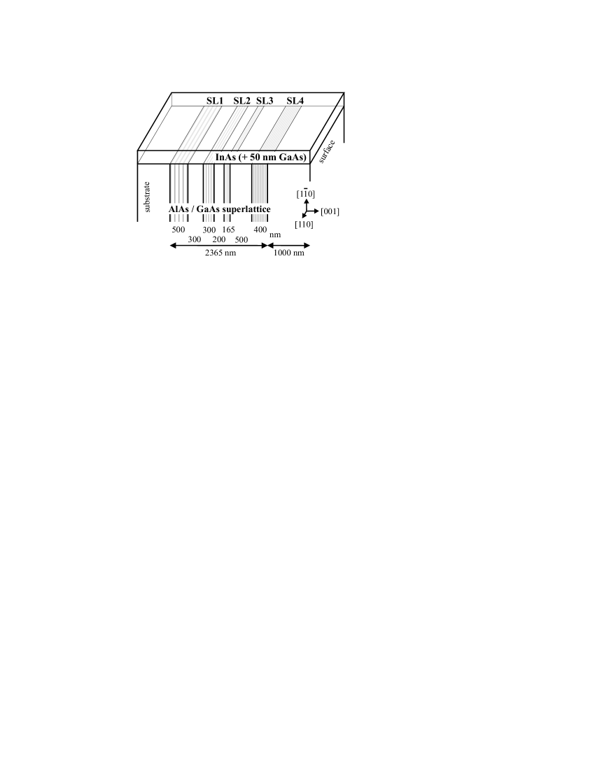
The sample investigated is depicted schematically in figure 1 and consists of 4 spatially separated AlAs/GaAs superlattices (SL1: 5 periods of 320 Å AlAs and 680 Å GaAs; SL2: 5 periods of 200 Å AlAs and 400 Å GaAs; SL3: 5 periods of 110 Å AlAs and 220 Å GaAs; SL4: 10 periods of 200 Å AlAs and 200 Å GaAs) grown on semi-insulating (001) GaAs. The substrate temperature during growth was 650 ∘C and the growth rates of both GaAs and AlAs were 1 Å/s under a III/V flux ratio between 3 and 6. Immediately after cleaving the substrate in the growth chamber, we deposited 3 ML InAs on the () surface. For samples designed for atomic force microscopy (AFM) investigations, growth was stopped after this step whereas for photoluminescence measurements, the InAs layer was covered with 500 Å GaAs to bury the quantum dot layer. Growth on the () surface was performed at 470 ∘C with an InAs growth rate of 0.1 Å/s.
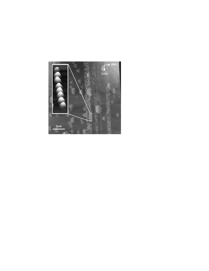
Figure 2 shows an AFM picture of the uncapped sample. Quantum dot-like nanostructures can clearly be identified above all four superlattice regions SL1–SL4 note:dotsnotseen . Most surprisingly, the AFM measurements clearly indicate nucleation of quantum dot-like nanostructures along the Al-rich regions of the exposed () growth surface. Furthermore, the typical size of the quantum dots is found to directly reflect the thickness of the underlying AlAs layer; being largest for SL1 (320 Å AlAs), smallest for SL3 (110 Å AlAs) and comparable for SL2 and SL4 which share a common AlAs width (200 Å) but differ in the thickness of the surrounding GaAs and in the total number of periods. However the quantum dots grown on SL2 and SL4 appear to have larger spatial and structural inhomogeneities. We conclude, therefore, that the geometric properties of the quantum dots are sensitive not only to the thickness of the underlying AlAs layer but also the surrounding GaAs plays an important role in the dot nucleation process. We suggest the following mechanism leading to dot growth on the () AlAs layers: due to the higher desorption rate of In atoms on GaAs compared with AlAs and the lower In adatom mobility on Al-containing layers note:alasmobility there is an effective mass flow towards the AlAs layers. On top of these layers, the strain due to the lattice mismatch between InAs and AlAs is reduced by the formation of a one-dimensional ordered array of quantum dots. The lower In adatom mobility on Al-rich surfaces may be the reason why strain is not reduced by dislocations, as known for InAs growth on (110)-oriented GaAs belk but by nucleating in quantum dots. In recent work, Wassermann et al. have also observed that the mechanism inhibiting quantum dot formation on (110) surfaces could be overcome by InAs deposition on (110) AlAs layers lyon .
In order to investigate the optical properties of the quantum dot nanostructures we performed scanning -photoluminescence (PL) spectroscopy on a subsequently grown sample with a GaAs capping layer. The sample was mounted in a liquid He cryostat with the quantum dot layer accessible for the excitation laser beam and the microscope to collect photoluminescence. A HeNe laser, focused on the () surface of the sample was used to excite the quantum dots and a confocal excitation and collection geometry provides a maximum spatial resolution of 1.5 m. The excitation spot was then raster scanned across the () surface of the sample to obtain a spatially and spectrally resolved image of the optical emission characteristics. Spectra, taken at a temperature of 10 K and recorded at different positions along the [] direction are presented in figure 3 as a grayscale map.
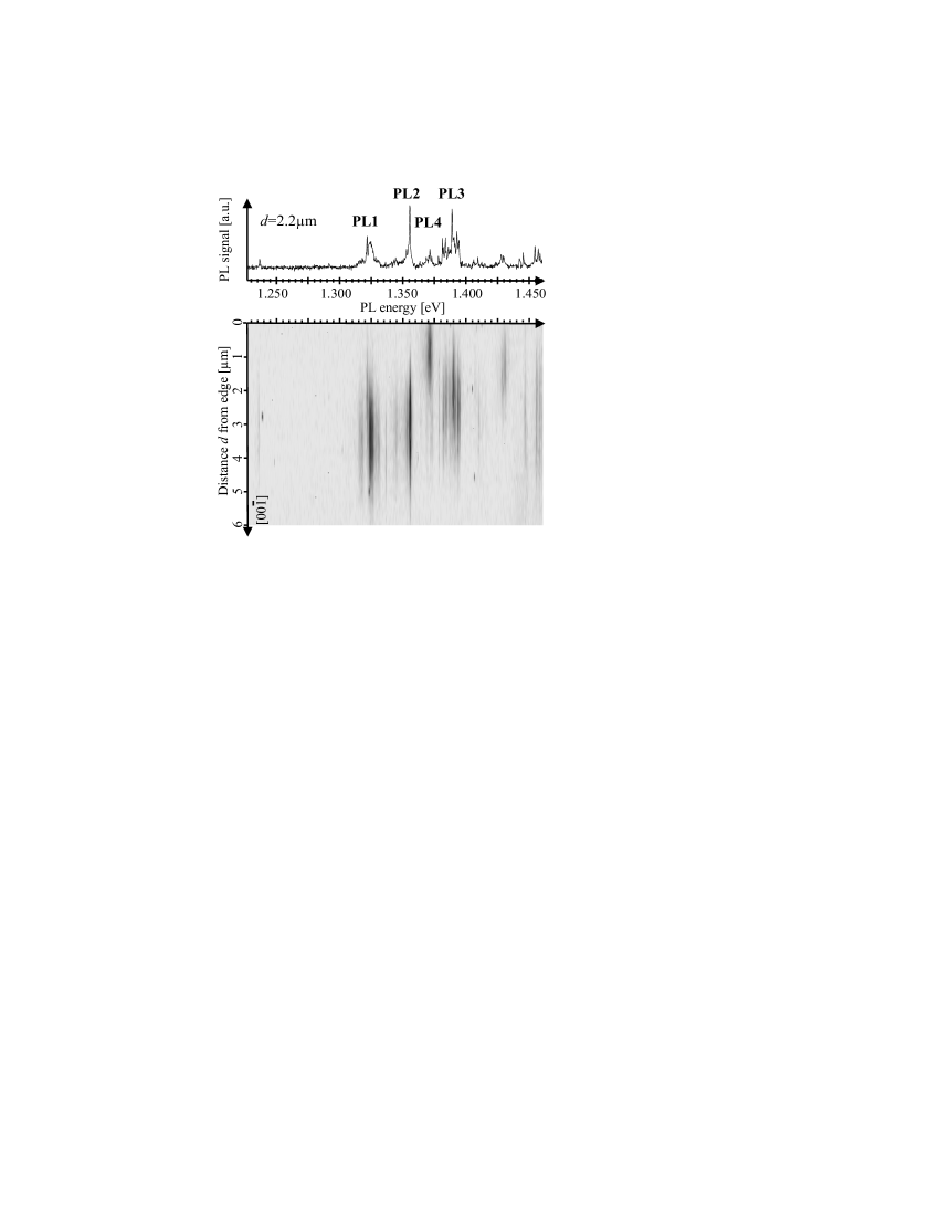
In this figure, four different groups of sharp QD-like photoluminescence (PL) peaks can be seen around 1.325 eV (PL1), 1.356 eV (PL2), 1.372 eV (PL4) and 1.389 eV (PL3). By examining the spatial distribution of these luminescence peaks and correcting for the spatial resolution of 1.5 m we deduced the positions on the () surface of the underlying luminescence centers. The positions obtained in this way and the distance between the luminescence center near the edge of the sample (PL4) and the most inner one (PL1) are in fairly good agreement with the geometric properties of the superlattice substrate (see Fig. 1). The PL signal labeled as group PL4 arises from a location next to the edge of the sample, and the group PL3 appears next as we traverse the [] direction towards bulk, unstructured substrate. Furthermore, the peaks of group PL3 show a higher PL energy compared to those in group PL4. Based on these observations we suggest that the PL signals of group PL4 belong to somewhat larger QDs grown on SL4 while the blue-shifted PL signals of group PL3 belong to smaller QDs nucleated above SL3. This suggestion is supported by the nominal thickness of the AlAs layers in the respective superlattices (SL3: 110 Å, SL4: 200 Å). According to the energies of the PL signals in group PL1 and PL2, we suggest that PL signals of group PL1 belong to the largest QDs grown on SL1 and that the PL signals of group PL2 belong to QDs nucleated above SL2. Additionally, the locations of the maximum intensities of the relevant peaks in these two groups are in very good agreement with the respective positions of SL1 and SL2 inside the sample. Photoluminescence spectra recorded from positions further from the edge of the sample revealed characteristically broader luminescence arising from the GaAs substrate but no sharp-line emission in the spectral window below 1.45 eV due to quantum dots. This observation strongly supports our identification of the sharp-line emission as arising from self-assembled quantum dots which are spatially ordered into one-dimensional arrays along the AlAs regions of the () surface as shown in figure 2.
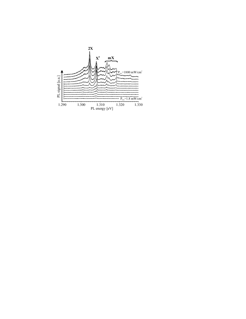
In order to further substantiate our assumption that the sharp-emission lines are due to laterally ordered self assembled quantum dots, we performed power dependent PL measurements at a specific position of SL1. The result of these measurements are summarized in figure 4. At low excitation power, just a single emission line at 1.308 eV is observed. The linear power dependence of this feature identifies it as arising from a single exciton (X0). In addition, this line is an emission doublet, possibly due to elongation of the quantum dots along the AlAs layer and the resulting electron-hole exchange interaction bayer . Upon increasing the excitation power density, several sharp lines at lower (1.3044 eV) and higher (1.3135 eV, 1.3148 eV, 1.3166 eV and 1.3182 eV) energies emerge. In particular, the intensity of the emission line at 1.3044 eV increases quadratically with excitation power density and dominates the spectra for the highest excitation densities investigated. This characteristic behavior identifies this peak as arising from bi-exciton (2X) recombination in the dot brunner , an observation which is further supported by the lineshape which, in contrast with the single exciton, exhibits no exchange splitting as expected from the spin-singlet nature of the bi-exciton ground state. The other lines arise from multi exciton complexes (mX) and charged excitons findeis .
In conclusion, we have demonstrated growth of long-range ordered arrays of self-assembled quantum dots on () GaAs. Both atomic force microscopy and photoluminescence experiments show that precise control of size and order is possible due to the underlying AlAs/GaAs superlattices. The fabricated quantum dots show excellent optical properties and have a high potential for realisation of well defined arrays of quantum dots with weak inhomogeneous broadening. A detailed analysis of the optimised growth conditions is currently in progress.
This work was supported financially by Deutsche Forschungsgemeinschaft via SFB 631 TP B1.
References
- (1) P. Ballet, J. B. Smathers, H. Yang, C. L. Workman, and G. J. Salamo, J. Appl. Phys. 90, 481 (2001).
- (2) R. Noetzel and K. H. Ploog, Journal of Crystal Growth 227–228, 8 (2001).
- (3) H. J. Kim, Y. J. Park, Y. M. Park, E. K. Kim, and T. W. Kim, Appl. Phys. Lett. 78, 3253 (2001).
- (4) R. Leon, S. Chaparro, S. R. Johnson, C. Navarro, X. Jin, Y. H. Zhang, J. Siegert, S. Marcinkevičius, X. Z. Liao, and J. Zou, J. Appl. Phys. 91, 5826 (2002).
- (5) B. D. Gerardot, G. Subramanian, S. Minvielle, H. Lee, J. A. Johnson, W. V. Schoenfeld, D. Pine, J. S. Speck, and P. M. Petroff, J. of Cryst. Growth 236, 647 (2002).
- (6) R. Songmuang, S. Kiravittaya, and O. G. Schmidt, Appl. Phys. Lett. 82, 2892 (2003).
- (7) L. Pfeiffer, K. W. West, H. L. Stormer, J. P. Eisenstein, K. W. Baldwin, D. Gershoni, and J. Spector, Appl. Phys. Lett. 56, 1697 (1990).
- (8) QDs on SL3 are to small to be resolved in this particular AFM picture shown here but were observed on the same sample by AFM with better resolution (not shown here).
- (9) this is known for InAs QD growth on (001)-oriented AlGaAs, see also Ref. ballet
- (10) J. G. Belk, D. W. Pashley, C. F. McConville, J. L. Sudijono, B. A. Joyce, and T. S. Jones, Phys. Rev. B 56, 10289 (1997).
- (11) D. Wasserman, S. A. Lyon, M. Hadjipanayi, A. Maciel, and J. F. Ryan, Appl. Phys. Lett. 83, 5050 (2003).
- (12) M. Bayer, G. Ortner, O. Stern, A. Kuther, A. A. Gorbunov, A. Forchel, P. Hawrylak, S. Fafard, K. Hinzer, T. L. Reinecke, S. N. Walck, J. P. Reithmaier, F. Klopf, and F. Schäfer, Phys. Rev. B 65, 195315 (2002).
- (13) K. Brunner, G. Abstreiter, G. Böhm, G. Tränkle, and G. Weimann, Phys. Rev. Lett. 73, 1138 (1994).
- (14) F. Findeis, A. Zrenner, G. Böhm, and G. Abstreiter, Solid State Comm. 114, 227 (2000).