Para to Ortho transition of metallic dimers on Si(001)
Abstract
Extensive electronic structure calculations are performed to obtain the stable geometries of metals like Al, Ga and In on the Si(001) surface at 0.5 ML and 1 ML coverages. Our results coupled with previous theoretical findings explain the recent experimental data in a comprehensive fashion. At low coverages, as shown by previous works, ‘Para’ dimers give the lowest energy structure. With increasing coverage beyond 0.5 ML, ‘Ortho’ dimers become part of low energy configurations leading toward a ‘Para’ to ‘Ortho’ transition at 1 ML coverage. For In mixed staggered dimers (‘Ortho’ and ‘Para’) give the lowest energy configuration. For Ga, mixed dimers are non-staggered, while for Al ‘Para’ to ‘Ortho’ transition of dimers is complete. Thus at intermediate coverages between 0.5 and 1 ML, the ‘Ortho’ and ‘Para’ dimers may coexist on the surface. Consequently, this may be an explanation of the fact that the experimental observations can be successfully interpreted using either orientation. A supported zigzag structure at 0.5 ML, which resembles , does not undergo a dimerization transition, and hence stays semi-metallic. Also, unlike the soliton formation is ruled out for this structure.
pacs:
73.63.-b, 73.90.+f, 68.90.+gI Introduction
The study of metals on semiconductors dates back to the nineteenth century and has seen a vigorous recent revival due to tremendous interest in Nanotechnology. Our ability to manipulate atoms, placing them at will on different surface sites to create exotic artificial structures, has led to further investigations dow of electronic and transport properties of free and supported nanowires. The placement of trivalent atoms (Al, Ga and In) on Si(001) can lead to the formation of low-dimensional structures, exhibiting significant new electronic properties.
One can easily compute the electronic properties of free standing nanowires. For this, one must first compute the total energy and determine the possible stable structures. Such calculations have indeed been carried out for nanowires por ; por1 ; tor ; tak ; hak ; sen ; ind1 consisting of a wide variety of atoms, e.g., K, Al, Cu, Ni, Au and Si. A general finding is that a zigzag structure in the form of an equilateral triangle is the most stable por ; por1 ; sen ; ind1 . This can be understood as arising primarily due to the maximization of coordination number for each atom in a quasi 1D structure. Another structure which also has a local minimum, but not terribly stable, is a wide angle isosceles triangle which somehow is reminiscent of the bulk environment. For example, Si which is a four fold coordinated in the bulk (tetrahedral angle ) shows ind1 a local minimum at an angle of . In general, free standing nanowires tend to be metallic (have bands crossing the Fermi level) but these nanowires in practice are to be supported. Silicon is the most widely used substrate for practical applications and the low index surfaces, Si(001) is the surface of choice. With the downward spiral toward nano devices, it is desirable to study the metallic properties at the lowest possible coverages. It is in this context that the study of metals like Al, Ga and In at submonolayer coverages on Si(001) take on the added importance. The interaction of metal nanowires with substrate can significantly alter the electronic properties.
Low-energy-electron-diffraction (LEED), Auger electron spectroscopy (AES) and Scanning tunneling microscopy (STM) studies have provided much informations about the interaction of Al, Ga and In overlayers on the Si(001) surface at different coverages and at different temperatures ide ; sakm ; bou ; knl ; nog1 ; nog2 ; bas1 ; bas2 ; sak1 ; sak2 ; sak3 ; sak4 .
Ide et al. ide observed 22, 23, 45, and 17 structures depending on the coverages less than 1 monolayer (ML) of Al on Si(001) and the substrate temperature in their LEED and AES experiments. However, the 22 and 23 phases were observed around 0.5 and 1/3 ML coverages respectively at low temperatures.
Sakamoto and Kawanami sakm performed Reflection high energy electron diffraction experiments and established the existence of phases with various symmetries (2 3, 2 5, 22 and 81) for Ga coverages less than 1 ML and at temperatures 350o C. Later, Bourguignon et al. bou examined the evolution of 1ML of Ga on Si(001) with LEED and observed all the above mentioned phases and in addition they also observed 12 phase at 1 ML coverage. Nogami et al. nog1 ; nog2 did STM studies and observed 22 at and below 0.5 ML coverage of Al, Ga and In on Si(001). Knall et al. knl performed experiment for In adsorption on Si(001) using RHED, LEED, AES and STM and observed transition from 22 to 21 structure of In as coverage increased. All the experimental results ide ; sakm ; bou ; knl ; nog1 ; nog2 ; bas1 ; bas2 ; sak1 ; sak2 ; sak3 ; sak4 point to the fact that at low temperatures Al, Ga and In form 22 structure on the Si(001) surface at 0.5 ML coverage.
At higher metal coverage, Nagomi et al. nog1 observed 3D island formation of Al on Si(001) around 1 ML coverage while ordered structures were observed for Ga and In on Si(001) at 1 ML coverage without any island formation bou ; knl . In particular, a 12 structure was observed for Ga, and 22, 21 structures were observed for In on Si(001). Since Ga does not form islands at 1ML coverage and it has been argued that Al forming islands at 1 ML coverage is unusual, we present a complete theoretical study for Al/Si(001) at 1 ML coverage.
Note that several experimental results were explained ide ; bou ; nog1 ; nog2 ; bas1 ; bas2 ; ind in terms of metal dimers oriented parallel to the Si dimer rows i.e. metal dimers were assumed to be directed perpendicular to the Si dimers in the reconstructed surface. This orientation of metal dimers is named as ‘Ortho’ dimers. Electronic structural calculations were done by Batra ind for Al on Si(001) at 0.5 ML coverage and he explained the experimentally observed patterns in terms of these ‘Ortho’ dimers. Later, Northrup et al. joh did theoretical calculations on the same system and showed that the orientation of metal dimers parallel to the Si dimers was most favorable. These dimers orientated parallel to the Si dimers are called as ‘Para’ dimers. A series of experiments sak1 ; sak2 ; sak3 performed recently for the structural configuration of metal dimers on the Si(001) surface indeed confirm the findings of Northrup et al. joh at 0.5 ML coverage. To the best of our knowledge, there is hardly any detailed theoretical study at higher coverages (1 ML) for these systems.
In this paper, we put significant effort to perform zero temperature electronic structural calculations for both 0.5 ML and 1 ML coverages of Al, Ga and In on the Si(001) surface and compare our results with the experimental and theoretical findings where available. We attempt to put the work in perspective and fill the holes by presenting new results. In particular, we find that our calculations at 0.5 ML give results in accord with Northrup’s predictions and also with the recent experimental results obtained by Sakama et al sak1 ; sak2 ; sak3 . More significantly, we obtain an orientational transition (‘Para’ to ‘Ortho’) for Al dimers as we go from 0.5 ML to 1 ML coverage. Our calculations also reveal that the reconstruction of Si(001) is completely lifted at 1 ML coverage of Al. We find that In and Ga interacts differently with the surface; for these metals the reconstruction is not lifted at 1 ML coverage. One finds the staggered mixed (‘Ortho’ and ‘Para’) dimers to be the lowest energy structure for In while the mixed dimers are non-staggered for Ga. The important conclusion is that the ‘Ortho’ dimers, which are energetically unfavorable at 0.5 ML coverage, become viable at higher coverage facilitating ‘Para’ to ‘Ortho’ transition as a function of coverage. Also, a previously reported semi-metallic phase of supported zigzag Al nanowire is found to be stable against a dimerizing Peierls transition unlike . The soliton sol formation in the supported nanowire is argued to be improbable.
The paper is organized as follows. The calculational parameters are given in sec. II and the results and discussions are presented in sec. III followed by a summary of our findings in sec. IV.
II Method
First principle total energy calculations were carried out within density functional theory at zero temperature using the VASP code kres . The wave functions are expressed by plane waves with the cutoff energy eV. The Brillouin Zone (BZ) integrations are performed by using the Monkhorst-Pack scheme with 441 -point meshes for 22 primitive cells. Ions are represented by ultra-soft Vanderbilt type pseudopotentials and results for fully relaxed atomic structures are obtained using the generalized gradient approximation (GGA). The preconditioned conjugate gradient method is used for the wave function optimization and the conjugate gradient method for ionic relaxation.
The Si(001) surface is represented by a repeated slab geometry. Each slab contains five Si atomic planes with Hydrogen atoms passivating the Si atoms at the bottom of the slab. Consecutive slabs are separated by a vacuum space of 9 Å. The Si atoms on the top four layer of the slab are allowed to relax while those in the bottom layer of the slab and the passivating Hydrogen atoms are kept fixed to simulate the bulk like termination. The convergence with respect to the energy cutoff and the number of points for similar structures has been established sen1 .
III results and discussions
We have performed total energy calculations using the above parameters for both the ideal and the reconstructed Si (001) surfaces. For the ideal case, the Si atoms on the surface are arranged in a square pattern of side 3.84 Å. For the reconstructed surface the Si atoms rearrange in such a way that the top layer Si atoms form dimer rows along the [10] direction but the atoms move along the [110] direction to form dimers. Here we consider 22 supercell for our calculations. At the 0.5 ML coverage of Al, Ga and In we start only with the reconstructed surface and at 1 ML coverage we start with both the ideal and reconstructed surfaces.
III.1 0.5 ML of coverage
Here we consider various structural arrangements of metal atoms on the Si(001) surface. The primitive cell contains two metal atoms which corresponds to 0.5 ML coverage. The results for Al/Si(001) are elaborated here and the results for Ga and In are briefly discussed. Two metal atoms in the cell may be placed in various ways on the surface. We consider several configurations to identify energetically the most favorable configuration. The configurations considered here are shown in the Fig. 1.

The metallic dimers configurations on reconstructed Si(001) shown in Figs. 1(a), 1(b) and 1(c) were considered by Batra ind . He found that the configuration in Fig. 1(b) was the most stable one followed by the configuration in Fig. 1(c). The configurations in Figs. 1(c) and 1(f) were considered by Northrup et al joh and they concluded that configuration in 1(f) was energetically the most favorable one. The arrangement in 1(c) is referred to as the ‘Ortho’ orientation of metal dimers and that in 1(f) is the ‘Para’ orientation of metal dimers as described earlier by the Northrup et al joh . In addition we consider two more configurations and they are shown in Figs. 1(d) and 1(e) respectively. The relative energies and the distance between the neighbor atoms for all the configurations are given in table I. All the energies are measured with respect to the reference energy which at 0.5 ML coverage of metal atoms correspond to the configuration shown in Fig. 2(a). For calculating the reference energy, all the Si atoms are held fixed and the metal atoms are allowed to relax along the [001] direction. The reference energies for the cases of Al, Ga, and In are -131.625 eV, -130.714 eV, and -130.255 eV. respectively. It is clear from table I that the configuration shown in 1(f) i.e., Al dimer placed between the Si dimer rows with ‘Para’ orientation has the lowest energy and hence the most favorable configuration. Our results support the calculations first made by Northrup et al joh and later by Brocks et alcar . We also observe that the next most favorable configuration is that shown in 1(e) which also has ‘Para’ orientation of Al dimer but the dimer is placed within a Si dimer row. However, the energy difference between these two configurations with ‘Para’ orientation of metal dimers is 1 eV. This is because the dimer within the Si row [1(e)] has to reside at much higher position compared to that placed between the dimer rows [1(f)] and hence has a weaker binding. We also note that the energy difference between the ‘Para’ and ‘Ortho’ orientation of dimers is even larger, the ‘Para’ being more stable 1.3 eV.

To calculate the potential energy variation of the system as a function of the Al dimer orientation, we place the Al dimer between the Si dimer rows at a fixed height and rotate about the [001] direction. The result is shown in Fig. 3. This shows two minima at ‘Ortho’ and ‘Para’ orientations respectively and there is a small barrier as one goes from ‘Ortho’ to ‘Para’ orientation. Therefore, the Al dimers take ‘Para’ orientation which is strongly more favorable compared to the ‘Ortho’ orientation. This result also agrees with the observation in a recent experiment by Sakama et al sak1 . We note that though the Si dimers are stretched by 0.26 Å the reconstruction of the Si surface is not lifted at 0.5 ML of coverage.
We have also done similar calculations for Ga and In adsorption on the reconstructed Si(001) surface and found that the ‘Para’ orientation of Ga and In dimers are also favored with relative energies -3.29 eV and -2.90 eV respectively. The results for Ga and In also agree with recent experimental results obtained by Sakama et al sak2 ; sak3 . The surface pattern at 0.5 ML coverage is 22. It is also clear that all the patterns observed at low temperatures and below 0.5 ML coverage of Al, Ga and In on the reconstructed Si(001) can be explained by the ‘Para’ dimers as proposed by Northrup joh , but contrary to the earlier proposal by Batra ind .

One focus of Batra’s work ind , however, was to find a stable metallic configuration for Al. He reported a zigzag nano-structure shown in Fig. 1(b) which he labeled as , as being stable with a local minimum in energy. Our present calculations support this finding except that we get Å in contrast to Batra’s value of Å. This overlayer structure of Al atoms is reminiscent of a uniform bond structure with the important difference that there is no direct Al-Al bond. The nearest neighbor Al-Al distance ( 4 Å) in the overlayer is much longer than the bulk Al-Al distance ( 2.8 Å) and they “see” each other only through the delocalized electrons in the -orbitals. In , C-C atoms are not only coupled through -electrons but they also form strong uniform -bonds leading to a semi-metallic structure. This structure becomes semi-conducting upon undergoing a bond alternation Peierls like transition to Double (D), Single (S), DS, DS … repeating pattern of bonds. It supports the soliton sol formation by creating a defective structure of the type .. DS, DS, SD, SD .. by having two single bonds adjacent to each other. The Al overlayer structureind2 has two electrons of each Al atom tied to a surface Si atom in an like fashion while the third electron of Al is in a free electron like state along the nanowire (-direction). Here X represents a surface Si atom which nominally has a single electron in a dangling -orbital available for bonding with Al. Interatomic distance between Al and surface Si atoms, d(Al-X) 2.4 Å, implies a strong bond. The delocalized electron (one per Al atom) creates a one dimensional semi-metallic system. Naturally, under such situation metallic wires may be realized and it will be conducting under small bias conditions. But then the standard Peierls distortion may come into play depending upon the strength of the surface bonds. Within the error of our calculations (estimated at 7 meV) we did not find any lowering of the total energy upon dimerization, unlike . In fact we noted that a dimerization of Al atoms in the zigzag structure by an amount Å raised the total energy by 0.1 eV. Thus the surface bonds formed by supported nanowires can lock the metallic structure in place. There is no possibility of a soliton formation in the Al overlayer structure because of the large Al-Al distance. However, it will be interesting to look for soliton behavior in other overlayers.
III.2 1 ML of coverage
We consider the adsorption of four metal atoms on the Si(001) surface of a 22 unit cell which corresponds to 1 ML coverage. Results for Al, Ga, and In on Si(001) are presented here. Various possible configurations considered are shown in Fig. 4. Here calculations are done for both the ideal and the reconstructed Si surfaces to find energetically the most favorable configuration. The 22 unit cells are bordered by thick lines in Fig. 4. The configurations considereed include Para-Para and Ortho-Ortho metal dimers on reconstructed (Figs. 4(a) - 4(d)) and Ideal (Figs. 4(e) - 4(h)) on Si(001) surface. In addition, we also consider mixed dimers (Ortho and Para) on reconstructed surfaces (Figs. 4(i) - 4(l)). Mixed dimers on ideal Si surface were not stable and readily caused the silicon surface to reconstruct.

The relative energies for the relaxed structures of Al, Ga and In on the reconstructed surfaces are given in table II for four possible configurations and the same on the ideal surfaces are shown in table III. The energies for the configurations with mixed dimers are given in table IV. The reference energies at 1 ML coverage of metal atoms are obtained for the configuration shown in Fig. 2(b) where all Si atoms are held fixed the metal atoms are allowed to relax along the (001) direction. The reference energies for the cases of Al, Ga and In are -137.963 eV, -136.485 eV and -136.044 eV respectively.
A general conclusion is that with increasing coverage beyond 0.5 ML, ‘Ortho’ dimers become part of the low energy configurations leading towards a ‘Para’ to ‘Ortho’ transition at 1 ML coverage. For In, mixed staggered dimers (‘Ortho’ and ‘Para’) give the lowest energy configuration. For Ga, mixed dimers are non-staggered, while for Al ‘Para’ to ‘Ortho’ transition of dimers is complete. This is an important conclusion because at or below 0.5 ML ‘Ortho’ dimers were not favorable. Also, the puzzle that ‘Ortho’ and ‘Para’ dimers are both seen is resolved due to the preponderance of ‘Ortho’ dimers at increasing coverages.
Let us first consider the structure consisting of Al dimers with ‘Para’ orientation as it was the most favorable structure at 0.5 ML coverage. Two configurations are possible with ‘Para’ orientation of Al dimers: (i) the configurations shown in Figs. 4(a) and 4(e) on the reconstructed and ideal surfaces respectively and (ii) the configurations shown in Figs. 4(b) and 4(f) on the reconstructed and ideal surfaces respectively. After complete relaxation, we note that the final low energy structure is independent of the initial surface pattern (reconstructed /ideal). When we start from an ideal surface, the Si atoms dimerize and the low energy structure is the one with reconstructed Si surface. Same final structure is achieved when we start form the reconstructed surface. Also note that the relaxed system with the staggered dimers configuration in 4(b) consisting of parallel dimers on the reconstructed surface is less favorable compared to that on the same reconstructed surface with the configuration in 4(a). Comparing 4(b) and 4(f) we find that the final energies of the systems differ by a large amount: staggered dimers on the ideal surface are least favorable.
Next we consider the configurations in 4(c) and 4(d). These structures are obtained by just rotating the Al dimers in 4(a) and 4(b) by 90 degree (i.e., dimers now take ‘Ortho’ orientation). From table II it is clear that these configurations are more favorable compared to those in 4(a) and 4(b). We find that after complete relaxation, the total energies and the structures of these two configurations become independent of the initial surface pattern.
In addition, we consider the configurations consisting of mixed dimers (‘Ortho’ and ‘Para’) as shown in Figs. 4(i) - 4(l). Similar configurations on ideal surface are unstable, the Si surface reconstructs itself and eventually leads to the configurations 4(i), 4(j) and 4(k). Again for Al, the configurations 4(j) and 4(l) are unstable. From table IV we see that the configuration with mixed Al dimers shown in Fig. 4(i) has a deep local minumum. This configuration is more favorable compared to the configurations consisting of only ‘Para’ orientation of Al dimers (i.e., Figs. 4(a) and 4(f)).
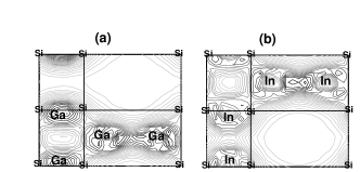
However, comparing the energies for configurations 4(i) and 4(g) we find that the lowest energy structure is the one shown in Fig. 4(g) where the reconstruction is completely lifted. All the Si bonds are saturated here. Since the reconstruction is completely lifted at 1 ML coverage, we conclude that the breaking of Si dimer bonds is initiated just beyond 0.5 ML of coverage. Most interestingly we note that an orientational transition for the Al dimers takes place as one goes from 0.5 ML coverage to 1 ML coverage: The Al dimers change their orientation from ‘Para’ to ‘Ortho’ after breaking the Si dimer bonds. This is also supported by the charge density plot for the lowest energy configurations at 0.5 and 1 ML coverage as shown in Figs. 5(a) and 5(b) respectively.

Earlier, it was argued that at 0.5 ML coverage all Si bonds are saturated and therefore beyond 0.5 ML coverage Al atoms may reside on top of each other and form 3D island. One experimental study observed the 3D island formation beyond 0.5 ML of Al coverage nog1 . Our calculation, however, suggests that for Al an orientational transition can take place at 1 ML coverage and the surface structure becomes regular having a 1 pattern where all bonds of Si and Al are saturated due to removal of the reconstruction of the Si surface. This leads us to speculate that further experiments on Al may seek out 12 pattern at 1 ML coverage. Furthermore, at coverages between 0.5 ML and 1 ML both the ‘Para’ and ‘Ortho’ Al dimers may coexist. This also clarifies why experiments at times have reported both ‘Para’ & ‘Ortho’ dimers because precise coverage is a difficult parameter to quantify.
Now we consider the Ga adsorption at 1 ML coverage. If we start with the reconstructed surface we find that the configuration in Fig. 4(i) with mixed dimers leads to the lowest energy structure where the reconstruction of the Si surface is not lifted during the relaxation process. The next best configuration is shown in Fig. 4(g) and consists of only ‘Ortho’ dimers. The structure remains ideal even after complete ionic relaxation. The configurations in Figs. 4(j) and 4(l) are unstable. Comparing final energies for various configurations on ideal and reconstructed surfaces we observe that the configuration in 4(i) is energetically the most favorable structure. Experiments indicate observing the 12 structure shown in 4(g) bou . Here the reconstruction of the Si surface is lifted, Ga dimers prefer ‘Ortho’ orientation leading to a 12 patten. Our calculations suggest that mixed dimers (Fig. 4(i)) and ‘Ortho’ dimers (Fig. 4(g)) as two contenders for the energy favored structures.
For the case of In we find that energetically the most favorable configuration is given in Fig. 4(j). This configuration corresponds to a 22 surface pattern. The configurations in Figs. 4(i) and 4(l) are unstable. More significantly, we note that the reconstruction of the surface is not lifted. We also find that the configurations consisting of ‘Para’ dimers (i.e., Figs. 4(a) and a(b)) are degenerate and energetically next favorable structures. The configurations in Figs. 4(a) and 4(b) correspond to the 21 and 22 surface structures respectively. Experimental results indicate the existence of both the 22 and 21 surface structures near 1 ML coverage of In. The most and the next favorable structures from our calculations are consistent with the experimentally observed 22 and 21 surface structures respectively.
To understand the bonding of Ga and In atoms on Si(001), the charge density distributions are plotted on the plane of metal atoms for the most favorable configurations at 1ML coverage of Ga and In and they are shown in Figs. 6(a) and 6(b) respectively. We observe that to a first approximation metal atoms display strong intra-plane bondings amongst themselves leaving the substrate in reconstructed state. The charge distribution in Fig. 6(b) also helps us to understand why the configuration 4(i) is unstable for In. In being larger in size, the In atoms in ‘Ortho’ orientation of configuration 4(i) are pushed away from each other to have a suitable coupling among In atoms and thus favoring the configuration 4(j) with (mixed) staggered dimers.
It is worth mentioning that one usually ends up with semi-metallic or non-metallic nanowires when supported on substrates as we saw above for the group III metals on Si(001). Very recently, there have been several important studies him1 ; him2 ; him3 ; him4 ; him5 of monovalent Au chains on various high indexed Si surfaces dealing with metallicity, Peierls distortion, charge density instability, fractional band fillings, and possibility of a spin charge separation due to the Luttinger-liquid phase. In fact, Himpsel and his group showed that Au nanowire supported on Si(553) is stable and it shows metallic behavior him1 ; him5 .
IV summary
We have done extensive total energy calculations for Al, Ga and In adsorption on the Si(001) surface at 0.5 and 1 ML coverages. The ‘Para’ orientation of dimers is the most stable orientation at 0.5 ML coverage for Al, Ga and In, which supports the results of Northrup et al and also agrees with the recent experimental observations. All the patterns observed in various experiments at low temperature and below 0.5 ML coverages can be explained by the ‘Para’ orientation of metal dimers. An interesting zigzag semi-metallic structure similar to is formed at 0.5 ML but is not the lowest energy structure. Soliton formation in overlayers is a fundamental topic for further study.
At 1 ML coverage a tendency towards the ‘Ortho’ orientation of dimers is noted. Thus we predict an orientational transition from ‘Para’ to ‘Ortho’ as we go from 0.5 ML to 1 ML coverage for Al and possibly Ga on the Si surface. In addition, the reconstruction of the Si surface is completely lifted at 1 ML coverage of Al. These results lead us to conclude that the surface patterns at 0.5 ML coverage can be explained in terms of ‘Para’ orientation of metal dimers and those at intermediate coverages between 0.5 and 1 ML may be explained by the co-existence of ‘Para’ and ‘Ortho’ orientation of dimers. For In mixed ‘Para’ and ‘Ortho’ dimers give the lowest energy configuration that exhibit 22 surface pattern and the transition is not complete.
References
- (1) P. A. Dowben, Surf. Sci. Rep. 40, 151 (2000).
- (2) D. S. Portal, E. Atracho, J. Junquera, P. Ordenjon, J. M. Soler, Phys. Rev. Lett. 83, 3884 (1999).
- (3) D. S. Portal, E. Atracho, J. Junquera, A. Garcia, and J. M. Soler, Surf. Sci, 482-485, 1261 (2001).
- (4) J. A. Torres, E. Tosatti, A. D. Coros, F. Ercolessi, J. J. Kohanoff, F. D. Di Tolla, and J. M. Soler, Surf. Sci. 426, L441 (1999).
- (5) M. Okamoto and K. Takayanagi, Phys. Rev. B 60, 7808 (1999).
- (6) H. Hakkinen, R. N. Barnett, U. Landman, J. Phys. Chem. B 103, 8814 (1999); H. Hakkinen, R. N. Barnett, A. G. Scherbakov, U. Landman, J. Phys. Chem B 104, 9063 (2000).
- (7) P. Sen, S. Ciraci, A. Budlum, and I. P. Batra, Phys. Rev. B 64, 195420 (2001).
- (8) I. P. Batra, T. Ciani, D. Boddupalli, and L. Soberano, Technical Preceedings of the 2003 Nanotechnology Conference and Trade Show, Shan Francisco, USA, 2, 206 (2003).
- (9) T. Ide, T Nishimori, and T. Ichinokawa, Surf. Sci. 209, 335 (1989).
- (10) T. Sakamoto and H. Kawanami, Surf. Sci. 111, 177 (1981)
- (11) B. Bourguignon, K. L. Carleton, and S. R. Leone, Surf. Sci. 204, 455 (1988).
- (12) J. Nogami, A. A. Baski, and C. F. Quate, Phys. Rev. B 44, 1415 (1991).
- (13) J. Nogami, Sang-il Park, and C. F. Quate, Appl. Phys. Lett. 53, 2086 (1988).
- (14) J. Knall, J. -E. Sundgren, G. V. Hansson, and J. E. Greene, Surf. Sci. 166, 512 (1986).
- (15) A. A. Baski, J. Nogami, and C. F. Quate, Phy. Rev. B 43, 9316 (1991).
- (16) A. A. Baski, J. Nogami, and C. F. Quate, J. Vac. Sci. Technol. A 8, 245 (1990); A 9, 1946 (1991).
- (17) H. Sakama, Ken-ichi Murakami, K. Nishikata, and A. Kawazu, Phys. Rev. B 48, 5278 (1993).
- (18) H. Sakama, Ken-ichi Murakami, K. Nishikata, and A. Kawazu, Phys. Rev. B 50, 14977 (1994).
- (19) H. Sakama, Ken-ichi Murakami, K. Nishikata, and A. Kawazu, Phys. Rev. B 53, 1080 (1996).
- (20) H. Sakama, A. Kawazu, T. Sueyoshi, T. Sato, and M. Iwatsuki, Phys. Rev. B 54, 8756 (1996).
- (21) I. P. Batra, Phys. Rev. Lett. 63, 1704 (1989).
- (22) J. E. Northrup, M. C. Schabel, C. J. Karlsson, and R. I. G. Uhrberg, Phys. Rev. B 44, 13799 (1991).
- (23) ‘Solitons and Fractional Charge in Quasi-One-Dimensional Conductors’ by J. R. Schrieffer in ‘Highlights of Condensed Matter Theory: Proceedings of the International School of Physics, Enrico Fermi, Course LXXXIX Varenna, Italy, June 28 - July 16, 1983’; edited by Bassani, Fumi and Tosi. Series: Enrico Fermi International Summar School Ser. Published by Elsevier (1985).
- (24) P. Sen, I. P. Batra, S. Sivananthan, and C. H. Grein, Phys. Rev. B, 68, 045314 (2003).
- (25) G. Brocks, P. J. Kelly, and R. Car, Phys. Rev. Lett. 70, 2786 (1993).
- (26) I. P. Batra, Phys. Rev. B 42, 9162 (1990).
- (27) G. Kresse and J. Hafner, Phys. Rev. B 47, R558 (1993); G. Kresse and J. Furtmuller, ibid. 54, 11169 (1996).
- (28) J. N. Crain, A. Kirakosian, K. N. Altmann, C. Bromberger, S. C. Erwin, J. L. McChesney, J. -L. Lin, and F. J. Himpsel, Phys. Rev. Lett. 90, 176805 (2003).
- (29) F. J. Himpsel, K. N. Altmann, R. Bennewitz, J. N. Crain, A. Kirakosian, J. -L. Lin, J. L. McChesney, J. Phys. Conden. Matt. 13, 11097 (2001).
- (30) I. K. Rabinson, P. A. Bennett, and F. J. Himpsel, Phys. Rev. Lett. 88, 096104 (2002).
- (31) K. N. Altmann, J. N. Crain, A. Kirakosian, J. -L. Lin, D. Y. Petrovykh, and F. J. Himpsel, Phys. Rev. B 64, 035406 (2001).
- (32) J. N. Crain, J. L. McChesney, Fan Zheng, M. C. Gallagher, P. C. Snijders, M. Bissen, C. Gundelach, S. C. Erwin, and F. J. Himpsel, ‘Gold Chain with Tailored Electronic States’, (unpublished ,2003).
| Configuration in figure 1 | Energy (eV) | d(Si-Si) | d(Si-Al) | d(Al-Al) | height |
| 1(a) | -1.892 | 2.52 | 2.67 | 3.84 | 1.36 |
| 1(b) | -1.951 | 2.46 | 2.50 | 4.01 | 1.40 |
| 1(c) | -2.216 | 2.78 | 2.62 | 2.64 | 0.73 |
| 1(d) | -2.153 | 2.59 | 2.39 | 2.60 | 1.92 |
| 1(e) | -2.499 | 2.45 | 2.47 | 2.62 | 1.55 |
| 1(f) | -3.482 | 2.44 | 2.48 | 2.67 | 1.10 |
| Configuration in figure 4 | Al: Energy (eV) | Ga: Energy (eV) | In: Energy (eV) |
|---|---|---|---|
| 4(a) | -2.680 (R) | -2.528 (R) | -2.077 (R) |
| 4(b) | -2.371 (R) | -2.448 (R) | -2.077 (R) |
| 4(c) | -3.092 (I) | -2.148 (R) | -1.441 (R) |
| 4(d) | -2.868 (I) | -2.187 (R) | -1.441 (R) |
| Configuration in figure 4 | Al: Energy (eV) | Ga: Energy (eV) | In: Energy (eV) |
|---|---|---|---|
| 4(e) | -2.680 (R) | -2.528 (R) | -1.840 (R) |
| 4(f) | -0.339 (I) | -0.427 (I) | 0.099 (I) |
| 4(g) | -3.092 (I) | -2.739 (I) | -0.389 (I) |
| 4(h) | -2.868 (I) | -2.631 (I) | -0.364 (I) |
| Configuration in figure 4 | Al: Energy (eV) | Ga: Energy (eV) | In: Energy (eV) |
|---|---|---|---|
| 4(i) | -2.937 (R) | -2.995 (R) | Unstable |
| 4(j) | Unstable | Unstable | -2.496 (R) |
| 4(k) | -2.667 (R) | -2.195 (R) | -1.886 (R) |
| 4(l) | Unstable | Unstable | Unstable |