On the Charge Ordering Observed by Recent STM Experiments
Abstract
We present a perspective on the recent discoveries of possible charge ordering in underdoped and by high-resolution scanning tunnelling spectroscopy.
In an STM study of optimally doped () at finite applied magnetic field, Hoffman et al discovered that in the vicinity of vortex cores the STM tunnelling conductance exhibits a checkerboard spatial dependencejenny , with Fourier peaks at and ( is the lattice constant of the copper oxide plane). Subsequently Howald et al studied optimally doped below at zero field, and reported observation of a nondispersive, directionally asymmetric tunneling conductance with Fourier peaks at and for low energies ()howald . However this result was not confirmed by later experimentshoffman ; kyle ; ali . In Ref.hoffman ; kyle ; ali high resolution STM studies of near-optimally doped below revealed rich bias-dependent quasiperiodic modulations of the STM tunnelling conductance. This phenomenon was explained as the quantum interference of quasiparticle de Broglie waveshoffman ; kyle ; wang . Ref.stevereview emphasized the deviation in the dispersion of the Fourier peaks in the and crystallographic directions from the simplest quasiparticle interference predictions.
In Ref.ali Vershinin et al have also reported results for . Interestingly, at low energies they observed bias-independent conductance modulations with Fourier peaks at and ali .
Two very recent low temperature STM experiments on underdoped stm1 and ()stm2 reported bias independent quasiperiodic modulations of the local conductance over a wide range of energy. These modulations have Fourier peaks at , with for , and for . Inspection of the real space modulation patterns shows that they are in phase upon bias reversalali ; stm1 ; stm2 . Ref.demler and Ref.zhang1 suggest that this bias symmetry contains vital information about the origin of these phenomena. Here we would like to point out that this symmetry could appear simply because the system is a doped Mott insulator. Indeed, doping a Mott insulator quite commonly transfers spectral weight (for both electrons and holes) proportional to the doping density from above the charge gap to low energy. As a result, when the doping density modulates in space, both the electron and hole spectral functions modulate with the same phase.
Despite the similarities between the phenomena reported in Ref.stm1 and Ref.stm2 , the and results are different in three important aspects. 1) The charge period for is not an integral multiple of the underlying lattice constant, while that of is. 2) For the modulation appears in spectrum only when , while in the signal appears right from zero bias. 3) For exhibits bias-dependent quasiparticle interference modulationhoffman , while such a signal is difficult to discern in . Due to these differences it is possible that the phenomenon observed in is due to true charge order, while that observed in is due to a yet-uncondensed charge orderstm1 ; stm2 .
The above STM experiments constitute an important set of observations concerning the electronic structure of the cuprates. The purpose of this paper is to present our interpretation of the results in Ref.jenny ; ali ; stm1 ; stm2 .
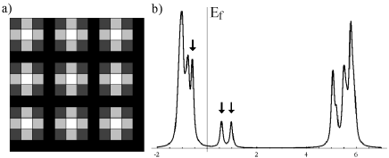
For , the modulation patterns consist of clearly visible unit cells over a wide range of bias voltages stm2 (). A caricature of the real space pattern seen in Ref.stm2 is shown in Fig.1a, where bright/dark marks regions of high/low differential conductance. In Ref.stm2 it is proposed that this spatial structure is due to the formation of a Wigner crystal of doped holes. In the following we corroborate this proposal with a theoretical analysis.
We start from a very underdoped situation where . This is the ideal doping density for a unit cell hole crystalhor . We interpret the bright region in each unit cell as having a high hole density (from a single hole delocalized in that region), and the dark region as having a low hole density. In the literature it has been proposed that doping a Mott insulator creates solitons (or spin bags/composite quasiparticles)spinbag ; bob ; gan . We believe that the above bright and dark regions reveal the internal structure of each soliton. Recently Chen et al proposed that at commensurate doping densities a Wigner crystal of hole pairs can formzhang . We believe that due to Coulomb repulsion such a state is energetically unstable. Moreover, even with a strong short-ranged attractive interaction to overcome the Coulomb interaction, we would expect segregation into hole-rich and hole-poor regions rather than crystallization of hole pairs.
To demonstrate the possibility of a soliton crystal we perform a variational study of the usual Hubbard model with Coulomb and nearest neighbor exchange interactions addednote ,
| (1) |
The variational ansatz we use is the most general Slater determinant which allows spatially inhomogeneous charge density, spin density, bond-current density, and superconducting pairing. Technically this is equivalent to factorizing the four-fermion terms in Eq. (1) into all possible quadratic combinations, and then solving the resulting quadratic Hamiltonian self-consistently. The following results are obtained numerically for an lattice with four holes and periodic boundary conditions.
It is quite encouraging that such a calculation does indeed yield a crystalline arrangement of the doped holes for a reasonable choice of parameters (, where is the repulsion energy two holes experience at the nearest neighbor distance)note2 . We have checked that as long as the Coulomb interaction exists, the stability of the soliton crystal is not affected by moderate modification of the above parameters. In all the cases we have studied the superconducting pairing and orbital current order are both absent when the holes crystallize. On the contrary we find that a non-zero antiferromagnetic order coexists with the hole crystal.
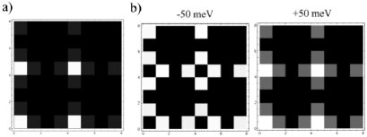
In Fig.1b we show the spatially averaged spectral function. The spectral peaks marked by arrows correspond to states whose wavefunctions are peaked at the soliton positions shown by the hole density (Fig.2a). The norm-squared wavefunctions of these states is reflected in the spatial variation of the local spectral function within of the Fermi level, as shown in Fig.2b. Although the detailed distribution of the spectral weight within the unit cell differs for the positive and negative bias, the gross structure (i.e. the fact that the overall spectral weight peaks near the soliton) is the same. In that regard the spatial structure is similar to that observed in Ref.stm2 . Contrary to experiment, in our calculation the dark region basically has the LDOS spectrum of the undoped insulator. We attribute the peak in the dark region seen in Ref.stm2 to the extra holes running on top of the Wigner crystal background which are absent in our calculation.
We also note that when a soliton is produced on a Neel background, its location (on the A or B sublattice of the antiferromagnetic order) depends on the spin of the removed electron. For example, if removing a spin up electron produces a soliton on the A sublattice, then removing a spin down electron will produce a soliton on the B sublattice. Moreover, our calculation shows that after removing an electron of a given spin, an electron of the opposite spin is always deeply bound to the soliton. This result is consistent with the notion that a soliton is a composite particle of a charged void and a spinbob .
A weakness of the above variational study is that it underestimates the quantum fluctuation of spins. To study the internal structure of each soliton more carefully, we diagonalize the t-J model on a plaquette with periodic boundary conditions. The Hamiltonian we use for this study is
| (2) |
In the following we choose , . Motivated by the experimental findings we restrict the hole to a plaquette in the unit cell. We compute the low-energy positive-biaswhy electron spectral function
| (3) |
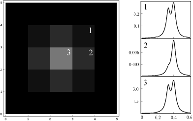
Here is the chemical potential, is the one-hole ground state with energy , and are the eigenstates of the half-filled system, with energy at most above the half-filled ground statehybridization . Fig.3 shows the hole density and at the three inequivalent sites of the central plaquette. The hole density displays a similar spatial structure to that seen in the Hubbard model calculation. The tunnelling spectrum at the brightest site (i.e. site 3) exhibits two peaks. To understand these two peaks we note that in a system the one-hole ground state is a spin doublet. The unpaired spin 1/2 is meant to mimic the dangling spin in the soliton. After the tunnelling process the spin from the added electron can form a singlet or a triplet with the original soliton spin. The lower(higher) peak corresponds to the lowest energy spin doublet spin singlet(triplet) transitions. The peaks seen in Fig.3 are similar to those observed in the bright region of the unit cell in Ref.stm2 . (Because we constrained the hole to the central region, we cannot address the peak observed in the dark region of the unit cell.)
In the above discussions we have concentrated on doping density , where the system is a charge insulator. The actual doping density in the sample studied in Ref.stm2 is likely to be higheruncertain . We assert that when deviates from the extra holes are delocalized on top of the Wigner crystal background. These mobile holes metallicize the system, and at low enough temperatures such a metal can become a superconductor. When that happens the Wigner crystal order coexists with superconductivity. Clearly an important question is the range of stability (in doping) of the Wigner crystal. Currently we do not have an explicit answer to this question. However, we emphasize that in answering this question the effects of lattice pinning (including the effect of periodic potential as well as elastic lattice relaxation) are extremely important. We propose that the unit cell Wigner crystal with extra mobile holes is adiabatically connected to the system with partially gapped Fermi surface near the antinodes discussed later in this paperzx .
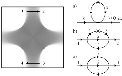
In the following we interpret the STM results for hoffman ; stm1 ; jenny ; ali . It is widely accepted that at optimal doping and lowest energies the only important elementary excitations are nodal quasiparticles. (The phase fluctuations are gapped due to the 3D Coulomb interaction.) As the excitation energy increases, antinodal quasiparticles and vortex-antivortex excitations join the list. The smallest vortex-antivortex pair is a roton, which appears as a (damped) pole of the dynamic density-density correlation function. Because the signatures of charge ordering at wavevectors are observed in the underdoped regime, we assert that there exist four discrete roton minima at wavevectors These roton minima enhance the DC charge susceptibility at . We believe that this enhancement is due to the particle-hole scattering across the nearly nested Fermi surface in the antinodal region (with nesting wavevector , see the left panel of Fig.4), so that .
Due to this enhancement, Friedel-like modulations in the electron density at are induced by disorder. These modulations can in turn scatter the quasiparticles and give rise to enhanced quasiparticle interference modulations at wavevector . The lowest order such process is illustrated in Fig.4awang ; others ; demler ; stevereview . We believe that the bias-independent local conductance modulations in Ref.jenny ; ali of optimally doped are due to the scattering described above.
In addition to Fig.4a the process depicted in Fig.4b can also scatter quasiparticles with momentum transfer . This process is resonantly enhanced if the quasiparticle energy is greater than the excitation energy of the rotonsubir . Given the fact that the modulation phenomenon in Ref.stm1 appears for , we think it quite likely it is due to the scattering process shown in Fig.4b. Finally, as pointed out by Zhou et alzhou , the process shown in Fig.4c (without impurity involvement) can be very effective in destroying the coherence of antinodal quasiparticle excitations in ARPES studiesarpes .
As a function of decreasing the roton minima deepen. When these minima touch zero, roton condensation occurs. This marks the onset of charge order. In an isotropic superfluid such as the onset of crystallization coincides with the loss of superfluidity. However, in a system like the where the charge order is commensurate with the underlying crystalline lattice, interstitial/vacancy superconductivity can coexist with Wigner crystal order due to lattice pinning effects. In such a coexistence phase, the antinodal quasiparticles are strongly scattered by , hence a gap can open up in the antinodal region. However since does not connect the nodes the nodal quasiparticles can remain gapless if the potential from charge order is not too strong. Under these conditions the nodal quasiparticle peak can survive in the ARPES spectrazxnaccoc . Upon further decreasing superconductivity eventually goes away. The loss of superconductivity is triggered by the Bose condensation of single vortices. With single vortices condensed all doped holes localize and the system becomes an insulator. After localization of holes the antiferromagnetic order is presumably restored. Because a real system has disorder, the Wigner crystal order discussed above can only have finite-range correlations due to the Imry-Ma physics.
Is the charge ordering discussed here and in Ref.ali ; stm1 ; stm2 responsible for the opening of the pseudogap? As has been pointed out in Ref.stm1 this crucially depends the relation between the charge freezing (crossover) temperature and the pseudogap temperature . If a strong argument can be made that the charge order actually drives the pseudogap formation. However, in our opinion it is likely that the pseudogap is caused by a different mechanism (e.g. spin singlet formation), and .
Finally, we note that like stripestranquada , the hole crystal discussed in this paper represents yet another form of charge order. We do not have much to say about how the system chooses one form or the other. What is important is that the cuprates seem to have a tendency to form some type of charge order. Whether these charge orders have anything to do with pairing is entirely unclear to us.
Acknowledgements: JCD and DHL would like to thank T.Hanaguri, J.E. Hoffman, E. Hudson, K. Lang, C. Lupien, K. McElroy, and R.Simmonds for numerous discussions. We thank A. Yazdani for valuable discussions and sharing his unpublished data with us. We also thank A. Lanzara, G.-H. Gweon, S.A. Kivelson, P.A. Lee, A. Seidel, Z.-X. Shen, and X.-J. Zhou for valuable discussions. DHL is supported by DOE grant DE-AC03-76SF00098. HF thanks Z. Hussain of the Advanced Light Source for support.
References
- (1) J.E. Hoffman, et al, Science 295,466 (2002).
- (2) C. Howald et al, Phys. Rev. B 67, 014533 (2003).
- (3) J. E. Hoffman, et al. Science 297, 1148 (2002).
- (4) K. McElroy, et al Nature 422, 520 (2003).
- (5) M. Vershinin et al, 10.1126/science.1093384 (Science Express Reports), February 12, 2004.
- (6) Q. Wang and D.-H. Lee, Phys. Rev. B 67, 020511 (2003).
- (7) S.A. Kivelson et al, Rev. Mod. Phys. 75 1201 (2003).
- (8) K. McElroy et al, to be published.
- (9) T. Hanaguri et al, submitted to Nature.
- (10) D. Podolsky, E. Demler, K. Damle and B.I. Halperin, Phys. Rev. B 67 94514 (2003).
- (11) H.-D. Chen et al, cond-mat/0402323.
- (12) F. Zhou et al, Supercond. Sci. Technol. 16, L7 (2003) proposes that cuprates may be charge ordered at commensurate doping densities.
- (13) J.R. Schrieffer, X.-G. Wen, S.-C.Zhang, Phys. Rev. Lett. 60 944 (1988).
- (14) P Beran et al Nucl. Phys. B, 473, 707 (1996); R.B. Laughlin, Phys. Rev. Lett. 79, 1726 (1997).
- (15) J. Gan, D-H Lee, P. Hedegård, Phys. Rev. B 54, 7737 (1996).
- (16) H.-D. Chen et al, Phys. Rev. Let. 89, 137004(2002); H-D. Chen et al, cond-mat/0312660.
- (17) We add the exchange term because without it the variational study precludes superconducting pairing.
- (18) Our choice of here is bigger than the widely accepted value in t-J model studies. This is because in the Hubbard model double occupancy is allowed. The extra charge fluctuation suppresses the effect of .
- (19) We focus on the positive bias because experimentally the local spectrum is basically featureless for negative bias.
- (20) To make the computation tractable, we first diagonalize the central plaquette and then hybridize its lowest energy states with the remaining spin sector of the system. In the one-hole(half-filled) sector we hybridize eigenstates of the plaquette which have energies within () of the ground state. For this reason, in Eq. (3) we only sum over eigenstates of the half-filled lattice with energy , where is the ground state energy of the half-filled lattice. For , the spectral function is not affected by changing the number of hybridized plaquette states.
- (21) The hole density is not precisely known because the sample surface doping may deviate from that in the bulk.
- (22) The existence of metallic charge density wave systems with partially gapped Fermi surface was emphasized to us by Z.-X. Shen.
- (23) L. Capriotti, D. J. Scalapino and R. D. Sedgewick. (available at http://xxx.lanl.gov/abs/cond-mat/0302563).
- (24) A similar scattering mechanism has been pointed out by A. Polkovnikov et al, Physica C, 19, 388-389, (2003).
- (25) X.-J. Zhou et al to appear in Phys. Rev. Lett.
- (26) A. Damascelli, Z. Hussain, Z-X, Shen, Rev. Mod. Phys. 75, 473 (2003) and references therein.
- (27) Y. Kohsaka et al, J. Phys. Soc. Jpn, 72 1018 (2003); F.Ronning et al, Phys. Rev. B 67, 165101 (2003).
- (28) J.M. Tranquada et al Nature 375, 561 (1995); J. Zaanen, O. Gunnarson Phys. Rev. B. 40, 7391 (1989); V.J. Emery, S.A. Kivelson Physica C 209, 597 (1993).