Spectroscopic imaging of single atoms within a bulk solid
Abstract
The ability to localize, identify and measure the electronic environment of individual atoms will provide fundamental insights into many issues in materials science, physics and nanotechnology. We demonstrate, using an aberration-corrected scanning transmission electron microscope, the spectroscopic imaging of single La atoms inside CaTiO3. Dynamical simulations confirm that the spectroscopic information is spatially confined around the scattering atom. Furthermore we show how the depth of the atom within the crystal may be estimated.
pacs:
61.14, 61.85Detection and measurement of the response of individual atoms has become a challenging issue to provide new insight into many fields in condensed matter and nanoscale sciences. Distributions of isolated atoms deeply modify the physical properties of many of the technologically most relevant and scientifically most interesting materials. Therefore, analytical techniques capable of probing single-atom identity and location are increasingly in demand. Here we show how the aberration-corrected scanning transmission electron microscope (STEM) allows not only the imaging of individual atoms inside a crystal, but their spectroscopic identification, with spatial resolution at the atomic scale. This substantial improvement in sensitivity opens up the possibility of probing the electronic environment of a single atom. Furthermore, by comparing signals from columns adjacent to that containing the single atom with dynamical simulations, the depth of the atom in the crystal can be estimated.
Much of the reported work on the identification and imaging of single atoms has been achieved by indirect techniques such as image simulation, including complex reconstruction of phase images with through focal series restoration Jia et al. (2003); Meyer et al. (2000). The STEM provides direct images of individual atoms as first demonstrated many years ago by the imaging of individual U and Th atoms on a thin carbon film Crewe et al. (1970). More recently, at a resolution of nm, the STEM has successfully imaged single atoms on and within a variety of materials, including catalysts Nellist and Pennycook (1996) and semiconductors Crewe et al. (1970); Voyles et al. (2002); Lupini and Pennycook (2003). Although the optics of the STEM is ideally suited to simultaneous imaging and spectroscopy, very few results have been reported that combine direct imaging with spectroscopic identification of individual atoms. Electron energy loss spectroscopy (EELS) signals also display high spatial resolution. Sub-unit cell analysis was first achieved by Spence and Lynch Spence and Lynch (1982) at 1.1 nm resolution. Single Gd atoms were for the first time identified by Suenaga and coworkers Suenaga et al. (2000) by combining phase contrast TEM imaging with EELS mapping in the STEM. However, their EELS resolution was only 0.6 nm, sufficient to resolve their widely spaced Gd atoms but insufficient to resolve the atomic structure of most materials. Scanning probe microscopies have also succeeded in achieving atomic-resolution spectroscopic identification of single atoms on surfaces, but they cannot probe individual atoms within the bulk environment.
Recent advances in aberration-corrected STEM provide the perfect scenario to address such a problem Dellby et al. (2001). A Z-contrast image is obtained by collecting, point by point, the Rutherford-scattered electrons at high angles using a high angle annular dark field (HAADF) detector. Energy loss electrons passing through the central hole in the detector can be collected simultaneously with the HAADF image. This correlation allows EELS to be performed with atomic resolution Browning et al. (1993); Duscher et al. (1998); Kaiser et al. (2003), limited only by the size of the probe Rafferty and Pennycook (1999); Allen et al. (2003a). Recently, by correcting the aberrations of the STEM probe-forming lens, a sub-Ångstrom beam has been demonstrated on a VG Microscopes HB501UX field emission STEM operating at 120 kV which is equipped with a Nion aberration corrector Batson et al. (2002). In a similar microscope, operated at 100 kV, a spatial resolution close to 0.11 nm is routinely achieved, and in this work we show how this enables us not only to image an individual atom within a crystal but to identify it spectroscopically.
The superlattice sample used for this study was a stack of CaTiO3 and LaxCa1-xTiO3 layers with a very low concentration of La dopants, prepared by pulsed laser deposition at ∘C, in an O2 pressure of mTorr, with a laser energy of J/cm2 at nm and a repetition rate of Hz. One commercial CaTiO3 target and a specially prepared LaxCa1-xTiO3 target with were used. The sample is epitaxial and highly ordered, and contains reference layers of La0.04Ca0.96TiO3 approximately 2.3 nm thick grown using shots of the La-doped target. Layers with correspondingly lower La concentrations were grown by using fewer shots, and were correspondingly thinner. From this calibration we calculate that a layer grown using just a single shot results in a La concentration of 1 atom per nm2. Assuming a typical TEM cross-section specimen to be about nm thick, on average, La atom should be found every 16 4 unit-cell columns. Simple statistical arguments yield a probability of only 3% that any given La-containing column contains more than one La atom. Such cross-section specimens were prepared by conventional methods. To minimize surface damage the final cleaning was performed by ion milling at 0.5 kV. Plasma cleaning was also used to prevent sample contamination.
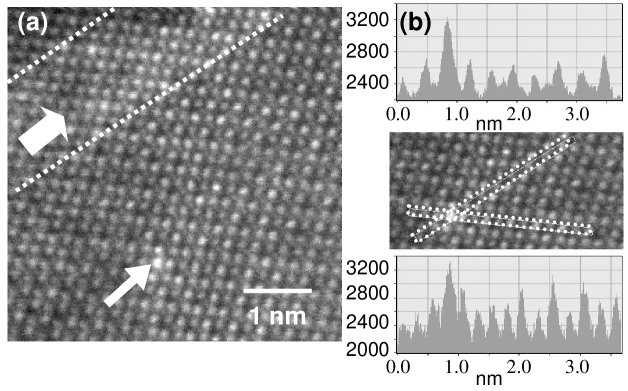
Figure 1 shows a high resolution Z-contrast image of a La0.002Ca0.998TiO3 layer adjacent to a thicker La0.04Ca0.96TiO3 layer. The higher atomic number of La, as opposed to Ca, O, or Ti, makes single La atoms appear as bright spots in this environment, although this brightness is dependent on atom depth Nellist and Pennycook (2000); Nakamura et al. (1997). Figure 1(b) shows the intensity traces across the atom. While we cannot completely exclude the possibility that any particular column contains two La atoms, many other single La atoms were imaged at different positions of the sample, in order to get better statistics, most giving an increase in columnar intensity by . They are seen to sit on the Ca site of the LaxCa1-xTiO3 perovskite structure, easily identifiable due to the fact that Ca columns appear darker than TiO columns.
Identification of the atoms was carried out using a McMullan design charge-coupled-device parallel-detection EELS system McMullan et al. (1990). This system does not provide optimized coupling from the aberration-corrected beam, having a collection efficiency of only 8%. [Collection efficiency is calculated as where = 7 mrad is the spectrometer entrance aperture, = 25 mrad is the probe forming aperture and is the characteristic angle of inelastic scattering for an energy loss and incident energy E0.] Nevertheless, by scanning the STEM probe directly over a highly magnified image of an isolated La atom (0.1 nm 0.1 nm in size as shown in figure 2), a clear EELS signature is obtained. In figure 2, spectrum 3 shows two distinct peaks that correspond to the La M4,5 lines at 832 and 849 eV. The intensity is low, as one would expect from the small number of counts associated with the excitations of a single atom, but clearly observable. The total number of M4,5 excitations for this spectrum is of the order of 104. To be certain that a single La atom can be detected, ten different bright spots were analyzed and each showed characteristic La lines with similar intensity. No meaningful beam damage was observed during the acquisition times employed, which were of the order of tenths of seconds.
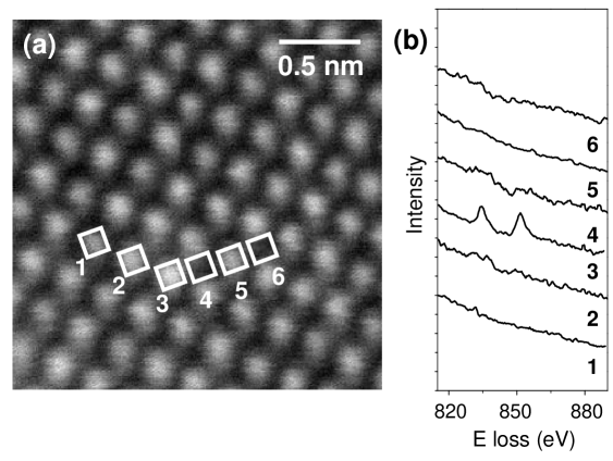
There has been much discussion about detection limits and the role that the delocalization of the underlying ionization process plays in limiting the resolution of the STEM image Spence and Lynch (1982); Rafferty and Pennycook (1999); Allen et al. (2003a); Kohl and Rose (1985); Muller and Silcox (1995); Holbrook and Bird (1995). To analyze the localization of the EELS signal we have taken spectra with the probe positioned on nearby columns as indicated on figure 2(a). Given the fact that neighboring atomic columns (2 and 4) correspond to different atomic species (TiO and O columns) the channeling and therefore the localization of the signal would be different. As depicted in figure 2(b), the EELS signal attributed to the La single atom is clearly localized on the atomic column containing this ion. When the electron beam is placed on adjacent columns the signal is substantially reduced, to only % on the neighboring TiO column (labeled 2), and to % on the neighboring O site (labeled 4), only 0.19 nm away. This clearly indicates that the La can be localized within significantly better than 0.2 nm, which is much larger than the impact parameter for La-M excitation Rafferty and Pennycook (1999) and therefore suggests that the residual intensity from neighboring columns is almost certainly the effect of channeling Allen et al. (2003b).
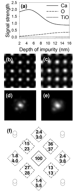
To explore the role of channeling, dynamical diffraction calculations were performed. Figure 3(a) shows the simulated La signal strength for an aberration-free probe situated on the Ca column, O column, and TiO column as a function of the impurity depth. A simplified cubic model for the structure suffices for this estimate, but subsequent calculations are based upon the distorted perovskite structure Buttner and Maslen (1992). The contribution on the Ca column initially increases due to the electrostatic attraction to the column (channeling), but then decreases as elastic and inelastic scattering mechanisms broaden the probe. The contribution on the O column rises gradually; simulations of the electron density make clear that this is due to probe spreading. From this figure it is estimated that a signal on the O column is obtained with an impurity depth of around 10 nm. The lack of any appreciable signal from the TiO column is an expression of the channeling strength of this column. To explain the % signal measured it must be appreciated that in the experiment the probe was not situated upon a single point but raster scanned across a highly magnified image. This introduces a finite, square scan region, of approximately 0.1 nm side length. Figures 3(b) and 3(c) show the HAADF images simulated Allen et al. (2003b); Findlay et al. (2003) for a 15 nm thick crystal using an aberration-free probe and an aberration-balanced probe respectively. The latter uses parameters measured from autotuning which, though recorded on a different occasion, can be regarded as typical. The latter image has been convolved with a Gaussian of half-width 0.04 nm, accounting for position instability of the probe and finite source size Nellist and Rodenburg (1994). EELS images were simulated using mixed dynamic form factor theory Findlay et al. (2003); Oxley and Allen (1998).
Figures 3(d) and 3(e) show EELS images corresponding to the parameters used in figures 3(b) and 3(c). The asymmetry of the structure, particularly whereby O columns distorted towards the Ca column provide a stronger signal than those distorted away from it, is evident. Figure 3(f) shows the scan regions and the signal strengths therein as a percentage of that on the Ca column. In these simulations the impurity was set at a depth of 12.2 nm. Note that the O column signal strength is on average higher than that of the experiment, and the TiO column signal strength is on average lower. For the second probe there are columns which agree with the experimental results to within the error bars. While the parameters used may not correspond precisely to those characterizing the experiment, the simulations have elucidated the mechanism by which the signals are obtained. The simulations support the localization of the ionization interaction and demonstrate that the dynamical propagation, in transferring some electron intensity to adjacent columns, is responsible for the signals obtained. The depth dependence seen in figure 3(a) is suggestive. It will be interesting to investigate how accurately the depth of an impurity atom may be determined in this fashion, particularly using larger probe-forming apertures and variable defocus.
In summary, an individual atom within a bulk solid has been identified spectroscopically with spatial resolution at the atomic level. This not only allows the detection and identification of single atoms, but also measurement of their electronic properties. Through dynamical simulations of probe spreading, an indication of atom depth is also obtained. Furthermore, the local formal oxidation state can be determined from the ratio of white line features present in L edges giving direct information about the magnetic moment and the valence of the atom. The present statistics are sufficient for such an analysis, although in this case the La ion is known to have a fixed 3+ valence state. However, optimum coupling of the aberration-corrected beam into the spectrometer would not only improve collection efficiency by over an order of magnitude, but also allow correction of spectrometer aberrations to give improved energy resolution Dellby et al. (2003). This would allow better comparison of local electronic structure with first-principles calculations Buczko et al. (2000).
There are many situations where the valence state of localized impurity atoms is variable, and it is very often the critical factor controlling macroscopic properties. Examples include band-bending effects at grain boundaries Kim et al. (2001); Hilgenkamp and Mannhart (2002), charge ordering in perovskite-based oxides Renner et al. (2002), charge-modulation superlattices Ohtomo et al. (2002), and molecular species in nanotubes Smith et al. (2000); Suenaga et al. (2003). We anticipate single atom analysis will open up many other areas of science where isolated atoms control macroscopic phenomena, including the origin of ductility or embrittlement in structural alloys, the nature of trap states at semiconductor interfaces, luminescent quantum efficiency in nanocrystals and active sites in heterogeneous catalysts.
The single atom represents the smallest quantum of matter that retains the characteristics of the material through its local electronic environment. The ability to probe the electronic structure of a material at this level represents the ultimate advance for understanding the atomic origins of materials properties. This work opens up this possibility.
M. Varela acknowledges fruitful discussions with R. Sanchez. Research of M. Varela is performed as a Eugene P. Wigner Fellow and staff member at ORNL. This research was sponsored by the Laboratory Directed Research and Development Program of ORNL, managed by UT-Battelle, LLC, for the U.S. Department of Energy under Contract No. DE-AC05-00OR22725 and by appointment to the ORNL Postdoctoral Research Program administered jointly by ORNL and ORISE. M. P. Oxley and L. J. Allen acknowledge support by the Australian Research Council.
References
- Jia et al. (2003) C. L. Jia, M. Lentzen, and K. Urban, Science 299, 870 (2003).
- Meyer et al. (2000) R. R. Meyer et al., Science 289, 1324 (2000).
- Crewe et al. (1970) A. V. Crewe, J. Wall, and J. Langmore, Science 168, 1338 (1970).
- Nellist and Pennycook (1996) P. D. Nellist and S. J. Pennycook, Science 274, 413 (1996).
- Voyles et al. (2002) P. M. Voyles et al., Nature 416, 826 (2002).
- Lupini and Pennycook (2003) A. R. Lupini and S. J. Pennycook, Ultramicroscopy 96, 313 (2003).
- Spence and Lynch (1982) J. C. H. Spence and J. Lynch, Ultramicroscopy 9, 267 (1982).
- Suenaga et al. (2000) K. Suenaga et al., Science 290, 2280 (2000).
- Dellby et al. (2001) N. Dellby et al., J. Electron Microsc. 50, 177 (2001).
- Browning et al. (1993) N. D. Browning, M. F. Chisholm, and S. J. Pennycook, Nature 366, 143 (1993).
- Duscher et al. (1998) G. Duscher, N. D. Browning, and S. J. Pennycook, Phys. Status Solidi A 166, 327 (1998).
- Kaiser et al. (2003) U. Kaiser et al., Nature Materials 1, 102 (2003).
- Rafferty and Pennycook (1999) B. Rafferty and S. J. Pennycook, Ultramicroscopy 78, 141 (1999).
- Allen et al. (2003a) L. J. Allen et al., Phys. Rev. Lett. 91, 105503 (2003a).
- Batson et al. (2002) P. E. Batson, N. Dellby, and O. L. Krivanek, Nature 418, 617 (2002).
- Nellist and Pennycook (2000) P. D. Nellist and S. J. Pennycook, Adv. Imaging and Electron Phys. 113, 147 (2000).
- Nakamura et al. (1997) K. Nakamura et al., J. Electron Microsc. 46, 33 (1997).
- McMullan et al. (1990) D. McMullan et al., in Proceedings of the Institute of Physics Electron Microscopy and Analysis Group and Royal Microscopical Society Conference, p. 55 (1990).
- Kohl and Rose (1985) H. Kohl and H. Rose, Adv. Imaging and Electron Phys. 65, 173 (1985).
- Muller and Silcox (1995) D. A. Muller and J. Silcox, Ultramicroscopy 59, 195 (1995).
- Holbrook and Bird (1995) O. F. Holbrook and D. M. Bird, in Proceedings of the Conference on Electron Microsopy and Analysis (1995), [Inst. Physics. Conf. Ser. 147,175 (1995)].
- Allen et al. (2003b) L. J. Allen et al., Ultramicroscopy 96, 47 (2003b).
- Buttner and Maslen (1992) R. H. Buttner and E. N. Maslen, Acta Crystallogr. B48, 644 (1992).
- Findlay et al. (2003) S. D. Findlay et al., Ultramicroscopy 96, 65 (2003).
- Nellist and Rodenburg (1994) P. D. Nellist and J. M. Rodenburg, Ultramicroscopy 54, 61 (1994).
- Oxley and Allen (1998) M. P. Oxley and L. J. Allen, Phys. Rev. B 57, 3273 (1998).
- Dellby et al. (2003) N. Dellby et al., Microscopy and Microanalysis (to be published) (2003).
- Buczko et al. (2000) R. Buczko et al., Phys. Rev. Lett. 85, 2168 (2000).
- Kim et al. (2001) M. Kim et al., Phys. Rev. Lett. 86, 4056 (2001).
- Hilgenkamp and Mannhart (2002) H. Hilgenkamp and J. Mannhart, Rev. Mod. Phys. 74, 485 (2002).
- Renner et al. (2002) C. Renner et al., Nature 416, 518 (2002).
- Ohtomo et al. (2002) A. Ohtomo et al., Nature 419, 378 (2002).
- Smith et al. (2000) B. W. Smith, D. E. Luzzi, and Y. Achiba, Chem. Phys. Lett. 331, 137 (2000).
- Suenaga et al. (2003) K. Suenaga et al., Phys. Rev. Lett. 90, 055506 (2003).