Measurement of the shear strength of a charge-density wave
Abstract
We have explored the shear plasticity of charge density waves (CDWs) in NbSe3 samples with cross-sections having a single micro-fabricated thickness step. Shear stresses along the step result from thickness-dependent CDW pinning. For small thickness differences the CDW depins elastically at the volume average depinning field. For large thickness differences the thicker, more weakly pinned side depins first via plastic shear, and shear plasticity contributes substantial dissipation well above the pinning force. A simple model describes the qualitative features of our data, and yields a value for the CDW’s shear strength of approximately Nm-2. This value is orders of magnitude smaller than the CDW’s longitudinal modulus but much larger than corresponding values for flux-line lattices, and in part explains the relative coherence of the CDW response.
pacs:
72.15.Nj,71.45.Lr,73.23.-b,74.25.QtThe elastic and plastic properties of driven periodic media including charge/spin density waves (CDWs/SDWs) feinberg , flux-line lattices in type-II superconductors blatter ; marchetti ; yoon and Wigner crystals andrei are central to understanding their rich dynamics and phase behavior. Impurities, dislocations and other disorder pin the periodic medium in each case, so that a minimum or threshold force must be applied to produce collective motion. Shear moduli are especially important because they determine the extent of shear plasticity. In experiments on moving flux-line lattices, shear plasticity dominates so that the coherent oscillations at the washboard frequency expected in a purely elastic system are replaced by an incoherent response with large -like noise clem , and vanishing of the shear modulus leads to liquid-like motion.
Shear plasticity also plays an important role in charge- and spin-density wave motion, rounding the depinning transition, broadening the spectral width of the coherent oscillations, and smearing out velocity steps caused by mode locking to an applied ac drive. Experiments show that this shear primarily results from meso/macroscopic sample inhomogeneities maher ; rare homogeneous samples of the CDW conductor NbSe3 show highly coherent washboard oscillations and complete harmonic and subharmonic mode locking thorne , suggesting that the intrinsic CDW response is nearly elastic.
Here we show that crystals with micro-fabricated steps running along the direction of CDW conduction show a non-monotonic variation of their depinning force with the size of the step, due to shear along the step. A simple model reproduces this variation, and allows us to determine the CDW’s shear strength to be Nm-2. This value is more than three orders of magnitude smaller than the shear elastic modulus dicarlo_adelman , and two orders of magnitude smaller than the contribution of the pinned CDW to the shear modulus of the crystal xiang . It is much larger than for flux-line lattices, which explains in part the relative coherence of the CDW response.
NbSe3 and related quasi-one-dimensional CDW materials grow as long thin ribbons. Shear usually results from steps in crystal thickness associated with small-angle grain boundaries that run along the ribbon () axis, which corresponds to the direction of CDW motion. Because typical crystal thicknesses are smaller than the CDW’s bulk phase correlation length in the thickness direction (m in undoped crystals), the depinning field varies inversely with crystal thickness yetman ; mccarten . As a result, thicker regions of the crystal cross-section have smaller depinning fields than thinner regions and tend to shear away from them, as illustrated in, e.g., Figures 3 and 4 of Li et al. li .
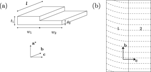
Detailed information about shear can be obtained by measuring the CDW response versus step height in samples with a single well-defined step, shown in Figure 1. The CDWs in rectangular regions 1 and 2 of thickness and have depinning fields and . They interact via a shear force along the direction of CDW motion at the interface between them. This force acts to retard motion of the thicker, more weakly pinned region 1 and assist motion of the thinner, more strongly pinned region 2.
If no slip occurs at the boundary (the static friction regime), then elastic coupling causes regions 1 and 2 depin at a common field given by
| (1) |
where and are the widths of regions 1 and 2, respectively. In thin crystals where and assuming , Eq. 1 reduces to .
The frictional force has a maximum static value , beyond which plastic slip occurs along the interface. The thick region 1 shears and slides relative to the thin region 2 at a field
| (2) |
where is the total CDW charge in region 1 which couples to the electric field. The maximum shear force should be proportional to the area of the interface between the two regions, and thus to . With fixed, Eq. 2 becomes
| (3) |
where is the plastic shear strength.
To study CDW shear, a NbSe3 crystal with a nearly rectangular cross-section is selected and placed on a substrate patterned with an array of non-perturbing gold electrical probes, each m wide in the direction of CDW motion. At least m of UV-5 resist is spun onto the crystal and substrate and then cured at C, the highest temperature to which the crystal is exposed during processing. The resist is patterned using a Cambridge-LEICA E-beam system 10.5. After developing, the pattern is etched into the sample using a CF4 dry plasma etch. The etch depth and spatial consistency can be monitored using the resistance per unit length for each probe pair along the sample. The average thickness is then calculated from the optically measured crystal width and NbSe3’s room temperature resistivity of m mccarten . More details on the fabrication process are found in oneill .
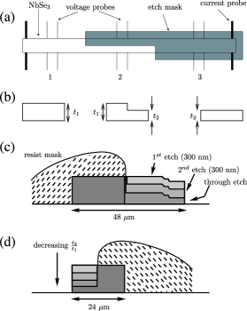
We explored two different sample designs. The first, shown in Figure 2(a) and (b), has three distinct cross-sections: an as-grown rectangular segment at one end with thickness , an etched rectangular segment at the other end with thickness , and a middle segment with a step running along separating unetched and etched regions of thickness and , respectively.
The second sample design, shown in Figure 2(c) and (d), is etched to produce a thickness step along its entire length. This eliminates current density changes and contributions to from longitudinal phase slip gill_maher present in the first design, and thus yields more precise measurements of shear effects on . The NbSe3 crystal used had two small steps. A portion of the crystal width containing the steps was thinned by repeated etching through the same resist mask, as shown in Figure 2(c), and transport measurements were performed after each etch. This yielded as a function of the thickness ratio . This process was then repeated using the remaining, initially step-free part of the crystal, as shown in Figure 2(d). Data for two samples, A and B, fabricated using the first and second process, respectively, are described here. Measurements were performed at where longitudinal phase slip contributions to are smallest. For both samples the thickness was less than the bulk CDW phase-phase correlation length in the direction, so that depinning fields are expected.
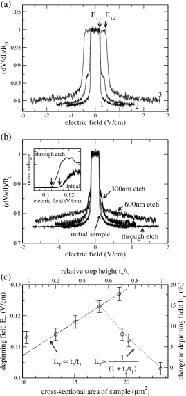
Figures 3(a) and 3(b) show the measured four-probe differential resistance versus electric field on Samples A and B, respectively. For Sample A, the unetched region 1 and uniformly etched region 3 have depinning fields in the ratio . This roughly matches the thickness ratio determined from room temperature resistance measurements. Consequently, despite producing a somewhat rougher surface, etching yields roughly the same thickness-dependent as is observed in unetched crystals of different thicknesses mccarten . Curve 2 in Figure 3(a) for the stepped segment 2 shows two separate depinnings for the etched and unetched portions of the crystal cross-section. The smaller depinning field of the unetched portion is increased only slightly from that of the unetched and step-free segment 1, suggesting that it shears from the etched portion. The larger depinning field of the thin, etched portion is lower than that of the unstepped etched segment 3, indicating that shear forces exerted by the depinned CDW in the thick portion assist depinning in the thin portion.
For Sample B, the normalized resistivities versus field in Figure 3(b) for the initial, unetched sample and for the through-etched sample are nearly identical and show a large, abrupt drop at , indicating excellent sample quality and that side-wall roughness induced by etching is unimportant. In contrast, for partial etching the differential resistance well above is significantly larger than for the unetched or through-etched sample, and grows with etch depth. The differential conductance associated with CDW motion at is 9% smaller for a nm etch depth () than for the through-etched crystal. This indicates that shear friction - in the form of shear-induced CDW phase vortex/dislocation “turbulence” - along the step strongly affects CDW dynamics.
To accurately determine how the depinning field of Sample B varies with etched thickness (), both the low-frequency noise amplitude and the differential resistance were measured versus electric field, as shown in Figure 3. The noise amplitude increases by orders of magnitude when the CDW or a portion of it depins fleming , and provides the most sensitive probe of . The cleanest data were obtained for the second etch sequence of Figure 2(d), starting with the rectangular cross-section produced in 2(c). To simplify interpretation, the widths of the etched and unetched portions were chosen to be nearly identical and equal to m.
Figure 3(c) shows the depinning field versus both sample cross-sectional area and thickness ratio . Although there is some scatter, the data clearly show two distinct regimes. For close to (small steps), increases with decreasing . For close to (large steps), increases with increasing . This general behavior is consistent with the simple model of Equations 1-3. For large etch thicknesses , the shear stress at the boundary between etched and unetched regions is small. drops sharply and smoothly, indicating that the entire sample volume depins at a unique , determined by the volume average of and given by Equation 1. As the etched thickness and decrease, the shear stress eventually is sufficient to cause shear slip along the boundary. In this case, shows two successive “drops” corresponding to depinning of the unetched (thick) and etched (thin) regions, respectively. The thick region’s depinning field is the sum of the pinning force in that region and the maximum retarding shear force exerted across the area of contact between the CDWs. This is determined by the maximum shear stress (force/area) times the contact area and is given by Equation 2.
The dotted and dashed lines in Figure 3(c) are fits to Eqns. 1 and 2 in the elastic and plastic regimes, respectively. The overall qualitative agreement is remarkable given the simplicity of our model. The elastic regime fit has no adjustable parameters, since for our undoped NbSe3 crystals has been determined in independent measurements mccarten , and is in good quantitative agreement as well. The CDW’s elastic shear stress along the boundary grows as becomes smaller. From the location of the cross-over between the elastic and plastic regimes we can estimate the CDW’s maximum elastic shear stress from Equation 3 as . Using the known cross-section dimensions , and , a condensate density cm-3, and the value of from the elastic fit at yields Nm-2. The plastic fit (dashed line) in Figure 3(c) is given by (in Vcm-1). From this fit we obtain the plastic shear strength at the interface between the thick and thin portions of the sample of Nm-2, in rough agreement with the maximum elastic shear strength. These estimates do not account for the effects of non uniform stresses along the interface due to the L-shaped cross-section.
A rough lower bound for the CDW’s shear modulus may be estimated from the ratio of the maximum elastic shear stress to the CDW shear strain when adjacent chains are out of phase. This gives the relation , where is the CDW wavelength and is the distance between adjacent chains smaalen . This gives Nm-2, more than orders of magnitude smaller than NbSe3’s measured longitudinal modulus Nm-2 dicarlo_adelman by the measured ratio of the longitudinal and transverse correlation lengths. As in ordinary crystals and flux-line lattices, the measured stress is likely reduced from its theoretical value by crystal and CDW defects.
The elastic moduli of flux-line lattices depend on magnetic field. The shear modulus increases roughly linearly at small fields, reaching a maximum at intermediate fields before dropping to zero at high fields. In Nb3Ge, the maximum value is Nm-2 at pruymboom . Measurements on vortices in nm-scale, weakly pinned Nb3Ge channels in a strongly pinned background pruymboom yield a maximum plastic shear strength at and of Nm-2. These shear modulus and shear strength values are roughly six and four orders of magnitude smaller, respectively, than the corresponding CDW values, consistent with the much more nearly elastic collective response of CDWs. The character of the bulk collective response depends on the ratio of the elastic strength to the bulk pinning strength, which is reflected in the ratio of the correlation length to the lattice periodicity. In CDW systems this ratio is typically to , two to three orders of magnitude larger than is typical in flux-line lattices.
In conclusion, we have observed a crossover from elastic to plastic behavior in the depinning of charge-density waves in crystals with artificially produced cross-section steps. From this behavior we have determined the shear strength of the CDW in NbSe3. This measurement provides a basis for understanding shear plasticity in CDW systems, and its relation to plasticity observed in other driven disordered media.
Acknowledgements.
We thank Rut Besseling for fruitful discussions. This work was supported by the National Science Foundation (NSF) (DMR 0101574 and INT 9812326). K. O’N. was supported by a U. S. Department of Education Fellowship. Nanofabrication work was performed at the Cornell Nano-Scale Science & Technology Facility, supported by the NSF(ECS-9731293), its users, and its industrial affiliates.References
- (1) D. Feinberg and J. Friedel, in Low-Dimensional Electronic Properties of Molybdenum Bronzes and Oxides, edited by C. Schlenker (Kluwer, Academic, Dordrecht, 1989), p. 407.
- (2) G. Blatter et al., Rev. Mod. Phys. 66, 1125 (1994).
- (3) M. C. Marchetti and D. R. Nelson, Physica C 330, 105 (2000); P. Benetatos and M. C. Marchetti, Phys. Rev. B 65, 134517 (2002).
- (4) S. Yoon et al., Science 255, 165 (1992); M. Marchevsky et al., Phys. Rev. B 57, 6061 (1998).
- (5) E. Y. Andrei et al., Phys. Rev. Lett. 60, 2765 (1988).
- (6) J. R. Clem, Phys. Rep. 75, 1 (1981).
- (7) M. P. Maher et al., Phys. Rev. B 43, 9968 (1991).
- (8) R. E. Thorne et al., Phys. Rev. B 35, 6348 (1987).
- (9) D. DiCarlo et al., Phys. Rev. Lett 70, 845 (1993); T. L. Adelman et al., Phys. Rev. B 52, R5483 (1995).
- (10) X. -D. Xiang and J. W. Brill, Phys. Rev. B 39, 1290 (1989).
- (11) P. J. Yetman and J. C. Gill, Solid State Commun., 62 (1987).
- (12) J. McCarten et al., Phys. Rev. B 46, 4456 (1992).
- (13) Y. Li et al., Phys. Rev. Lett. 83, 3514 (1999). X-ray images indicate that shear strains at thickness steps are much larger than those associated with pinning and contact effects at the temperatures studied here.
- (14) K. O’Neill et al., J. Phys. IV 12, 185 (2002).
- (15) J. C. Gill, J. Phys. C 19, 6589 (1986); M. P. Maher et al., Phys. Rev. B 52, 13850 (1995).
- (16) R. M. Fleming and C. C. Grimes, Phys. Rev. Lett. 42, 1423 (1979).
- (17) S. van Smaalen et al., Phys. Rev. B 45, 3103 (1992).
- (18) A. Pruymboom et al., Phys. Rev. Lett. 60, 1430 (1988); R. Besseling et al., Europhys. Lett. 62, 419 (2003).