Electronic structure of wurtzite and zinc-blende AlN
Abstract
The electronic structure of AlN in wurtzite and zinc-blende phases is studied experimentally and theoretically. By using x-ray emission spectroscopy, the Al , Al and N spectral densities are obtained. The corresponding local and partial theoretical densities of states (DOS), as well as the total DOS and the band structure, are calculated by using the full potential linearized augmented plane wave method, within the framework of the density functional theory. There is a relatively good agreement between the experimental spectra and the theoretical DOS, showing a large hybridization of the valence states all along the valence band. The discrepancies between the experimental and theoretical DOS, appearing towards the high binding energies, are ascribed to an underestimation of the valence band width in the calculations. Differences between the wurtzite and zinc-blende phases are small and reflect the slight variations between the atomic arrangements of both phases.
pacs:
78.70.En; 71.20.Nr; 71.15.MbI Introduction
The III-nitrides are nowadays widely used by the semiconductor industry. With respect to ”classical” III-V semiconductors, the nitrides have larger band gaps and stronger bonds. This makes them attractive for optoelectronic devices that need short wavelength of the visible range (violet and blue regions), for devices that work at high temperatures or with high powers. Among them, AlN has the largest band gap (6.2 eV) and thus, is the best material for constructing devices for the violet region. Moreover, with GaN, it can form GaxAl1-xN ternary alloys, with . This enables the tuning of the emission wavelength of the optoelectronic devices by choosing a suitable composition of the alloy.
AlN can be grown in wurtzite (WZ) or zinc-blende (ZB) phase. The stable one is the WZ phase, while the ZB phase is metastable. The optical gap of the WZ phase is direct and that of the ZB phase is indirect. This can be useful in constructing different kinds of quantum wells or superlattices. However, the growing of AlN is still a difficult task [1], particularly for the ZB phase. Due to the lack of good quality samples, only little work was done to study the physical properties of both phases. In the present work, we experimentally study the electronic structure of well characterized samples of both AlN phases, and compare the results with our theoretical calculations of the valence density of states (DOS).
The experimental electronic structure is obtained by x-ray emission spectroscopy (XES) induced by electrons. XES has been widely used to study the electronic structure of III-V semiconductors [2]. The DOS are calculated by using the full potential linearized augmented plane wave method, within the framework of the density functional theory (DFT) [3]. The experimental and theoretical determination of the various partial and local DOS is important for the study of the hybridization of the states inside the valence band.
II Experimental details
A Sample preparation
1 Wurtzite AlN
A 300 nm thick wurtzite AlN film is grown by molecular beam epitaxy (MBE) in a RIBER Compact 21 system, using ammonia as the N precursor, and standard solid sources for the group-III elements. The substrates is a 2” diameter Si (111) wafer with no ex-situ surface preparation. The in-situ silicon wafers cleaning involves a prolonged heating (about 10 hours) at 600∘C with subsequent removal of the oxide layer by rapid thermal annealing up to about 1000∘C. As followed by reflection high energy electron diffraction (RHEED), the appearance of the ( surface reconstruction indicates that the surface is clean and well ordered. The AlN layer is grown at about 920∘C. The set of growth parameters (mainly growth temperature and growth rate) is properly adjusted in order to rapidly obtain a layer by layer growth. This is achieved by using a very low growth rate (0.1 mm/h), and a nucleation temperature of 650∘C followed by a rapid ramping to the growth temperature (920∘C). The AlN RHEED pattern evolution during growth indicates that the growth first follows a three-dimensional mode, and progressively becomes two-dimensional (2D) after some tenths of nanometers. By decreasing the temperature after the growth, a surface reconstruction characteristic of the Al polarity is observed.
The structural quality of AlN films is investigated by transmission electron microscopy (TEM), x-ray diffraction (XRD) and atomic force microscopy (AFM). Measurements of the rms roughness by AFM give values of 0.4 nm. Cross-sectional TEM images show that the interface between AlN and the silicon substrate is sharp, and no amorphous interfacial layer can be observed. However a very high threading and misfit dislocations density is present due to the large lattice mismatch between AlN and Si. The dislocation density in the AlN layer is estimated from plan-view TEM images, and is about cm-2. During the cooling after the growth, an extensive stress appears due to the large thermal mismatch between Si and the AlN layer. This is confirmed by XRD measurements, which show an out-of-plane deformation of 2.2%.
2 Zinc-blende AlN
The sample is grown by plasma-assisted MBE. The metal fluxes are provided by conventional effusion cells, while active nitrogen results from radio frequency dissociation of N2 using a plasma cell. The used pseudo-substrate consists of a 3 m thick 3C-SiC layer grown by chemical vapor deposition on a Si(100) substrate [4]. To follow the evolution of the surface morphology, the growth is monitored in situ by RHEED. A smooth 2D-layer of zinc-blende AlN, with a thickness of about 300 nm, is obtained for a growth temperature of 720∘C under stoichiometric conditions. The roughness profile of AlN, deduced from (1 mm 1 mm) topographic AFM images, shows superficial steps with a maximum height of 0.8 nm. The structural quality of the AlN buffer layer is checked by high resolution x-ray diffraction study [5], and the purity of the cubic crystallographic phase is assessed by Raman spectroscopy measurements [6].
B X-ray emission spectroscopy
1 Studied emissions
In XES, one observes the radiative transitions towards a hole present in a core shell. The energy distribution of the emitted photons (called spectral density) is proportional to the convolution of the DOS of the initial and final states, weighted by the matrix element of the transition probability, and by the cube of the photon energy [7]. If the transition involves the valence band, the observed spectral density describes the valence DOS, broadened by a Lorentzian that represents the lifetime broadening of the initial state (i.e. a hole in a core shell) and a bell shape function representing the instrumental function. This is true only if the radiative transition probability does not vary strongly across the valence band, which is generally a good assumption. Because of the local character of the core hole wavefunction describing the initial state and of the dipole selection rules (), the observed DOS are local, i.e., in a compound the DOS is decomposed for each element, and partial, i.e., each -like symmetry of the DOS is obtained separately.
To study the occupied valence states of AlN, the following emission bands are analyzed :
-
-
the Al K emission ( transition), describing the Al states;
-
-
the Al L2,3 emission ( transition), describing the Al and states;
-
-
the N K emission ( transition), describing the N states.
When compared with the theoretical DOS, the experimental spectral densities are set on a binding energy scale relative to the top of the valence band, EV. This energy cannot be deduced from the combination of the XES experiments and the binding energies of the various core levels involved in the emissions. Indeed, the binding energies are determined by photoemission with respect to the Fermi level, EF, whose position with respect to EV is not known, and some states present in the AlN optical gap can induce a large shift of EF. The binding energy scale for the spectral densities is obtained by adjusting the main feature of the experimental and theoretical DOS, leading to an uncertainty of 0.3 eV in the position of EV. For the ultra-soft x-ray emissions, the variation of the photon energy must be taken into account. Then, the Al spectral density is divided by the cube of the photon energy. For the other emissions this correction is small enough to be omitted.
2 Experiment
The Al K emission is obtained using a curved crystal Johann-type x-ray spectrometer [8], with a quartz crystal curved with a radius of 500 mm. The spectral resolution, , is about 3000. The Al L2,3 and N K emissions are obtained using a 2 m grazing incidence (1.5∘) x-ray spectrometer [9], with a 600 grooves/mm grating. The N K emission is obtained in the third order of diffraction. The spectral resolution is about 1000 for the N K photon energy range, and about 750 for the Al L2,3 photon energy range.
The Al L2,3 and N K emissions are induced by a 3 keV electron beam, and the Al K emission by a 4 keV electron beam. Under these conditions the analyzed thickness is around hundred nanometers. For such a thickness, the samples can be considered as bulk. Since the electron current densities employed are low (about 1 mA/cm2), no damage can be induced inside the sample by the electron beam. Indeed, we verify that no evolution in time of the spectral shape and intensity occurs during data acquisition.
III Computational details
The calculations are performed using the full-potential linearized-augmented-plane-wave method, within the framework of the DFT, as implemented in the WIEN2k package [10]. This method has proved successful in the determination of the electronic structure of AlN [11]. Generalized gradient approximation (GGA) corrections to the local exchange-correlation functional are used as proposed by Perdew-Burke-Ernzerhof [12]. The GGA has been successfully used to study different phases of ionic compounds [13, 14].
The atomic structure is fixed to the experimental one for both phases. No geometry optimization is performed. The muffin-tin radii of the N and Al spheres are chosen as 1.677 and 1.877 Bohr, respectively. The -integration over the Brillouin zone is performed on a mesh for the WZ phase, and on a mesh for the ZB phase, leading to 400 and 446 irreducible points in the Brillouin zone, respectively.
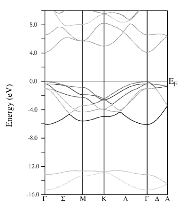
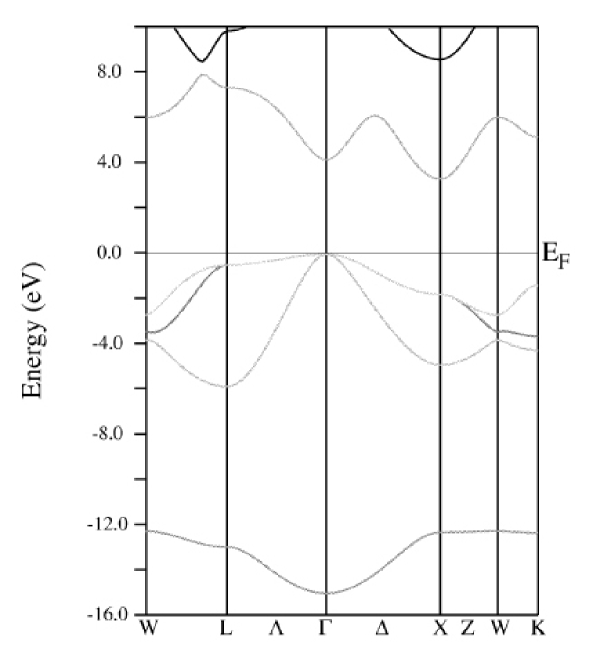
The calculated band structures for the WZ and ZB phases are presented in the Figures 1 and 2, respectively. It can be seen that the gap of WZ AlN is direct and that of ZB AlN is indirect, between the and points. This description is in agreement with calculations performed on both WZ and ZB phases, using the DFT and the local density approximation [11, 15, 16], or using an empirical pseudopotential approach [17].
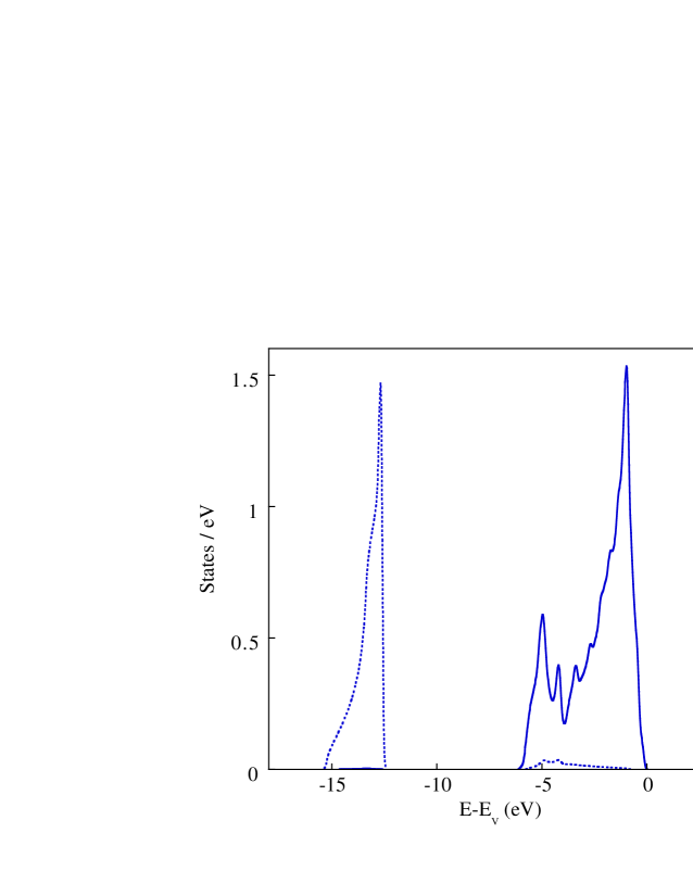
In Figure 3 the total DOS for WZ and ZB AlN are presented on a binding energy scale relative to . The calculated DOS are in agreement with previous calculations performed for these phases [18, 11]. The occupied valence states are distributed in two parts : in the lower valence band (LVB) towards the high binding energies, and in the upper valence band (UVB) towards the low binding energies. The calculated optical band gaps are 4.4 eV and 3.1 eV for WZ and ZB AlN, respectively. As expected from DFT calculations, these values are somewhat lower than the experimental values of 6.2 and 5.4 eV [19] for WZ and ZB AlN, respectively.
When compared to the XES experiments, the local and partial DOS are
-
-
weighted by the matrix element of the corresponding transition,
-
-
broadened by a Voigt function to take into account the instrumental function,
-
-
broadened by a Lorentzian function to take into account the lifetime of the core hole,
-
-
broadened by a Lorentzian of variable width to take into account the variable lifetime of the hole in the valence band. The valence hole width, , varies from 0 eV at , to 1 eV at the bottom of the valence band, , following :
where is the position of the hole within the valence band.
The DOS, which have been treated by this procedure, are called calculated spectra hereafter.
IV Experimental results and calculations
A Al spectral densities
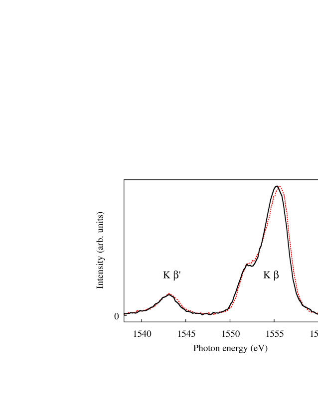
The Al spectral densities of WZ and ZB AlN are presented in Fig. 4a, on a photon energy scale. They are normalized with respect to their maximum. They present a main peak (labeled K) at about 1555 eV with a shoulder around 1552 eV. A secondary peak (labeled K) is observed at about 1548 eV. The shape and relative intensity of the WZ phase is almost in perfect agreement with a previous experiment [20]. Another experiment [21] obtained with a poorer spectral resolution is also in agreement with the presented spectra. Two other experiments [22, 23] can be found in the literature, but they strongly disagree with the presented spectrum. Since they show supplementary structures, which cannot be explained by DOS calculations (see below), these spectra were probably obtained from poor quality samples.
The differences observed between the spectra of the two AlN phases are small, Fig. 4a. With respect to the WZ phase, the maximum and the top of the valence band of the ZB phase are shifted towards the low photon energies, by 0.3 eV and 0.2 eV, respectively. The shoulder is slightly less intense for the ZB phase. A small difference is also noted on the K structure, which is narrower towards the high photon energies for the ZB phase.
The theoretical Al DOS for AlN WZ and ZB are presented in Fig. 4b. The differences between the two phases are rather small in the occupied states. The calculations are in agreement with previous local and partial DOS calculated for AlN WZ and ZB [18, 11].
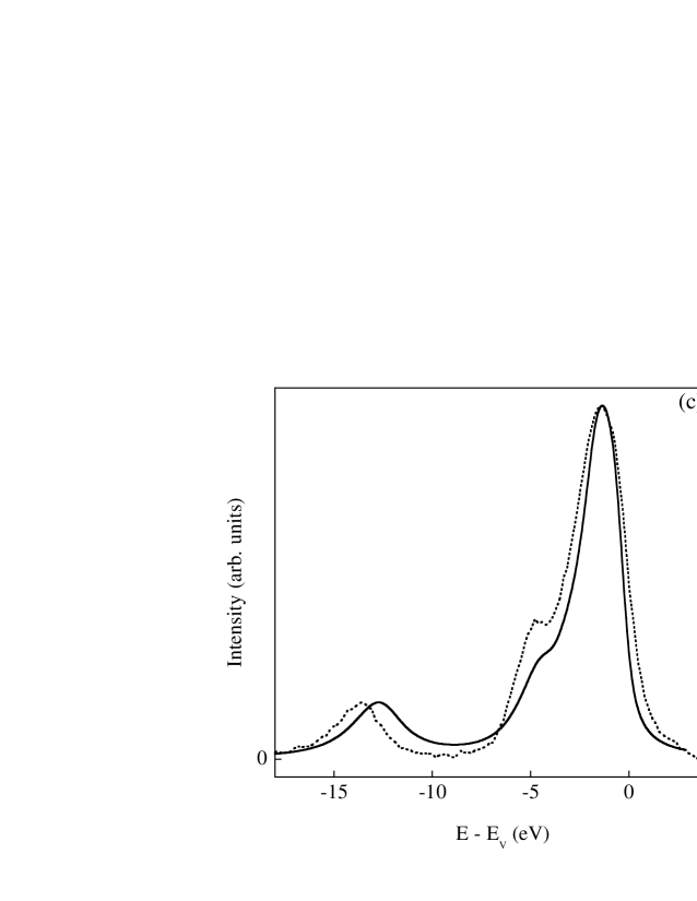
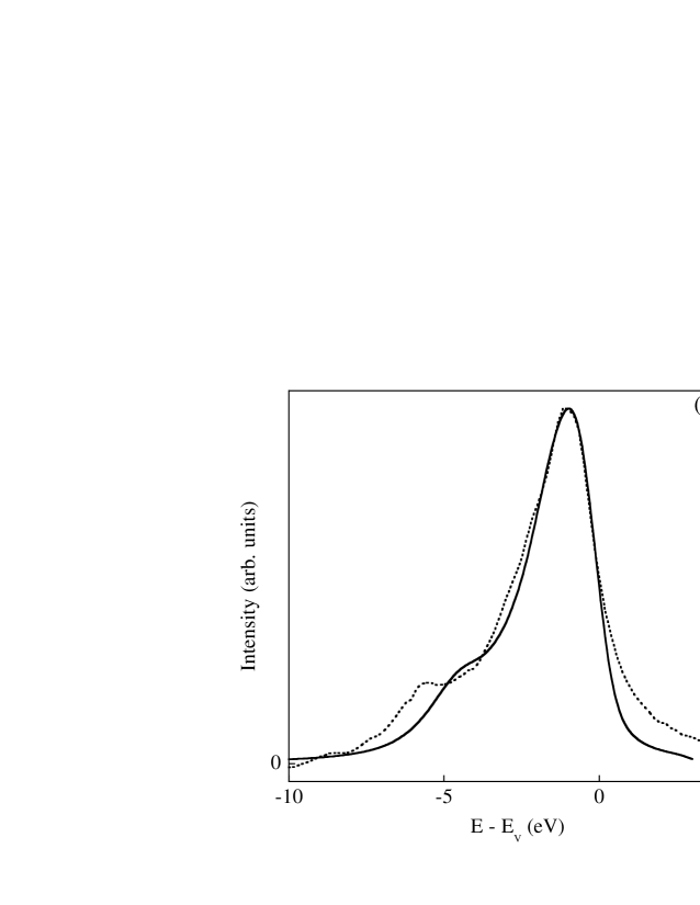
The comparison of the Al spectral density with the corresponding calculated spectrum is show in Fig. 4c for AlN ZB. It can be seen that the K and K ranges correspond to the UVB and the LVB, respectively. There is a satisfactory agreement between the experimental and theoretical DOS. In particular, the energy difference between the main peak and its shoulder is well reproduced. However, their relative intensity is different in the experiment and the theory. Another discrepancy can be noted for the K structure : in the theoretical DOS, this structure is shifted by 1 eV towards the lower binding energies, with respect to the experimental structure. Comparison between the experimental and theoretical DOS of AlN WZ leads to similar remarks.
B Al spectral densities
The Al spectral densities of WZ and ZB AlN are presented in Fig. 5a, on a photon energy scale. They are normalized with respect to their maximum. They present a doubly structured peak, with maxima at 65 and 68 eV. The spectrum of the WZ phase is in very good agreement with that presented in Ref. [20]. Another spectrum of WZ AlN can be found in the literature [22], but with a poorer resolution. With respect to the WZ phase, the peak towards the high photon energies is of lower intensity for the ZB phase.
The theoretical Al and DOS AlN WZ and ZB are presented on a binding energy scale relative to the top of the valence band in Fig. 5b. The calculations are in agreement with previous local and partial DOS calculated for AlN WZ and ZB [18, 11]. The differences between both phases are small. It is deduced that the maximum at 65 eV on the spectral DOS corresponds essentially to Al states, whereas Al and states contribute to the maximum at 68 eV.
For AlN ZB, the Al spectral density is compared to the calculated spectrum in Fig. 5c. It is observed that the positions of the two peaks agree in the experiment and the calculation, but the relative intensities of these peaks are not well reproduced by the calculation. However, it should be emphasized that the evolution of these relative intensities between the WZ and ZB phases, is correctly described by the calculation.
C N spectral densities
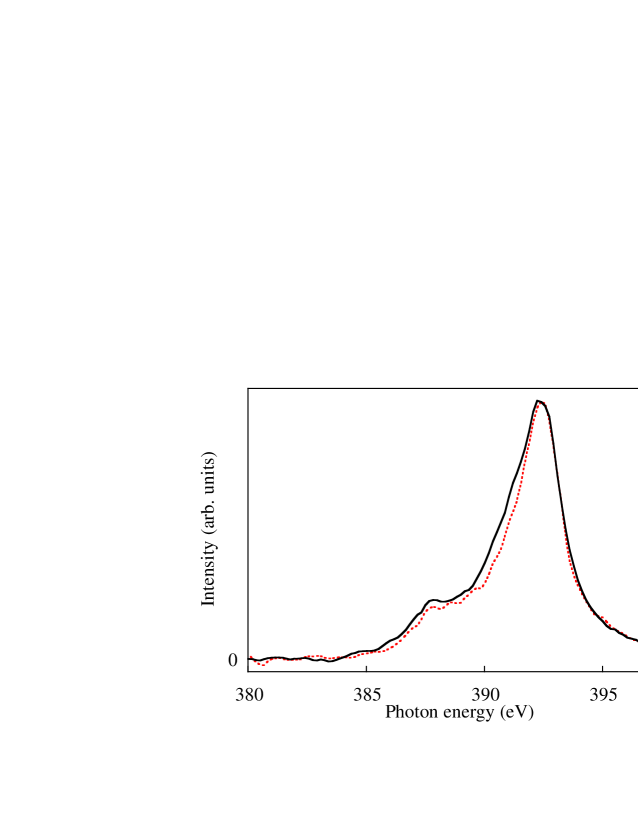
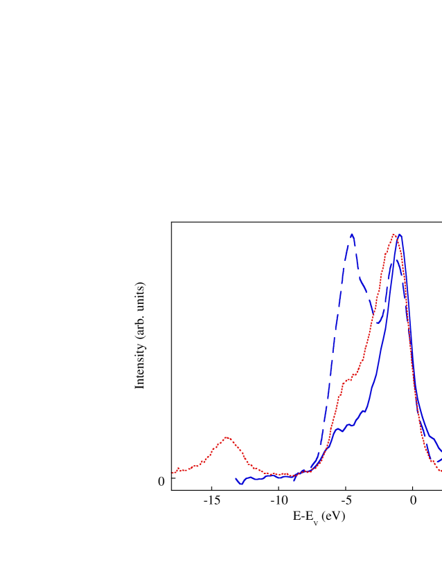
The N spectral densities of WZ and ZB AlN are presented in Fig. 6a, on a photon energy scale. They are normalized with respect to their maximum. They present a peak at about 392 eV, having a shoulder around 388 eV. The spectrum of the wurtzite phase is in good agreement with the spectra found in the litterature [22, 23, 24, 18]. With respect to the WZ phase, the emission band is narrower towards the low photon energies for the ZB phase. The valence band edges are the same for both phases.
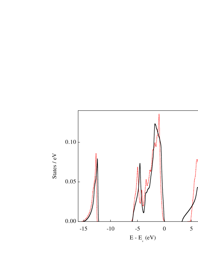
The occupied theoretical N DOS presents a large maximum at a binding energy of about -1 eV and a second maximum at -5 eV. The difference between the WZ and ZB phases are small. The calculations are in agreement with previous local and partial DOS calculated for AlN WZ and ZB [18, 11].
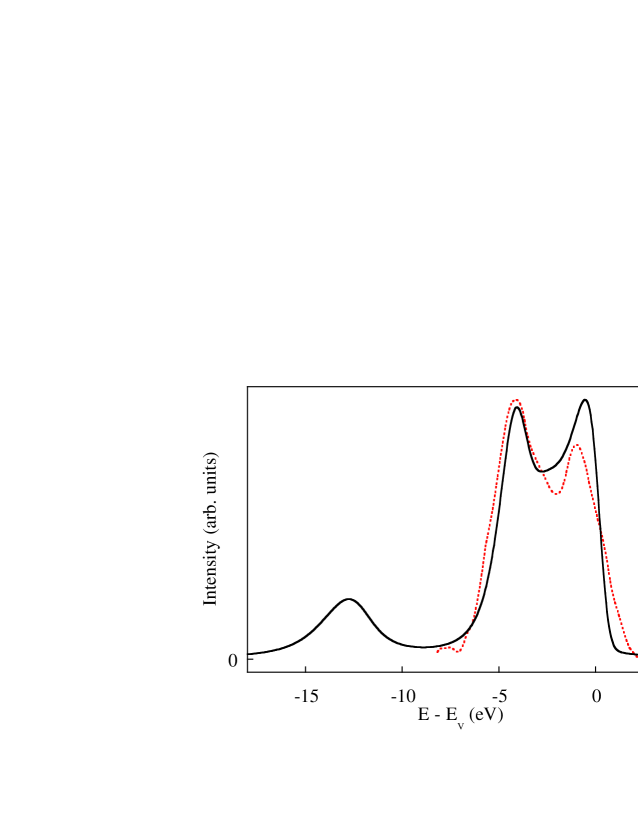
The comparison of the N spectral density with the calculated spectrum is shown in Fig. 6c for AlN ZB. The region of the maximum of the experimental DOS is well reproduced by the calculation. However, the experimental shoulder energy is about 1 eV higher than the calculated one. The DOS of AlN WZ presents the same situation.
V Discussion
The local atomic arrangement of the hexagonal WZ and cubic ZB AlN is as follows [25]. In both phases the Al atoms are in a tetrahedral environment. In the ZB phase, the distance between the Al atom and the first four N neighbors is 0.175 nm, and the angle formed by a N atom and two of its Al nearest neighbors is 109.5∘ (perfect tetrahedron). In the WZ phase, there are two kinds of N nearest neighbors, surrounding the Al atoms inside a slightly distorted tetrahedron, located at 0.189 and 0.192 nm. This leads to two different angles of 117.7∘ and 107.7∘. There is also a difference concerning the second neighbor cation-anion bond distances : 12 equivalents in ZB AlN, and 10 of three kinds in WZ AlN.
Since the XES is a local probe, the method is more sensitive to changes involving the nearest neighbors than to those due to differences in the long range interactions. When the structural environment varies between two phases, pronounced changes of the DOS shapes are observed. This is the case, for example, for -alumina (Al atoms in octahedral environment) and -alumina (Al atoms both in octahedral and tetrahedral environments) [26]. For AlN, interactions between the first neighbors are about the same for the WZ and ZB phases, and one expects DOS changes to be smaller than those seen in the example cited above. In fact, no change is observed for the N spectral densities in the higher part of the valence band, and changes concerning the Al and Al spectral densities are limited. In fact, the changes mainly involve the Al states that are situated towards the lower binding energies, owing to their largely extended character.
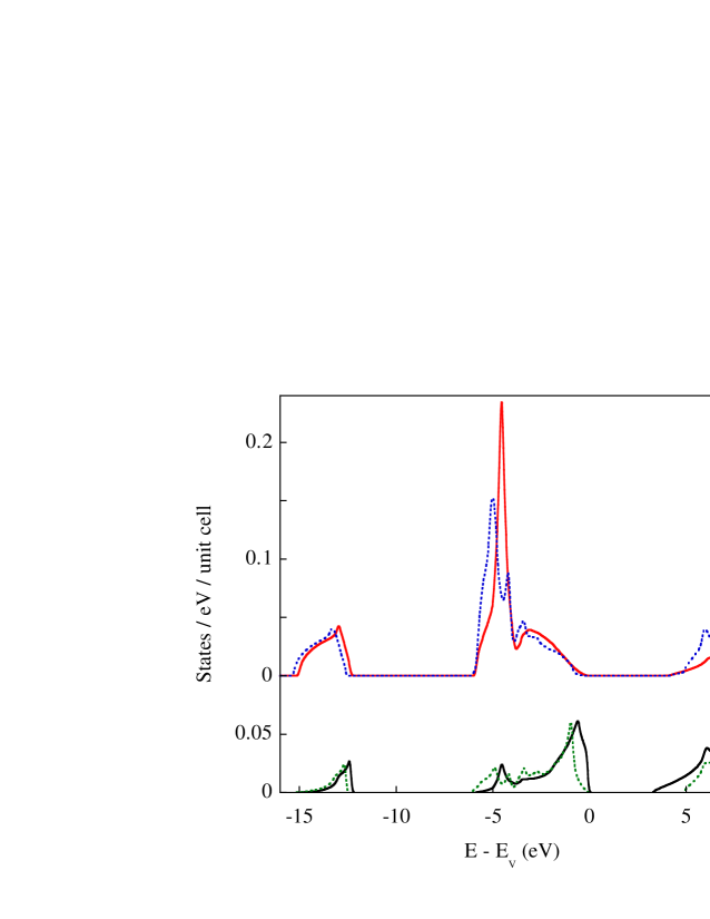
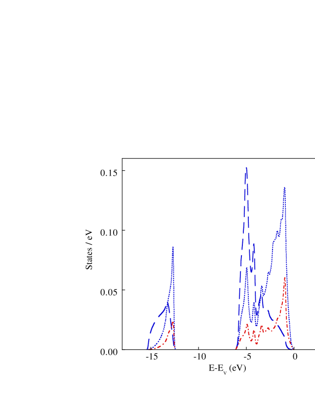
An important characteristic of the DOS for this kind of materials is the strong mixing between the various states constituting the valence band. This is borne out in Fig. 7a, where the Al , Al and N spectral densities of WZ AlN are presented together on a binding energy scale relative to the top of the valence band. It can be seen that the occupied valence states are hybridized all along the valence band. Concerning the UVB, its top is dominated by the strongly mixed N and Al states, and its bottom by the N and Al ones. The maximum of the Al distribution and the shoulders of the Al and N distributions are in correspondence around -6 eV. This energy distribution of the states within the valence band is in agreement with the DOS calculations, Fig. 7b and c.
In the region of the LVB, centered around -14 eV, only the Al states are observed. A maximum of the Al spectral density has been seen in Ref. [20] at the same experimental binding energy. According to Fig. 7b and c, all the different kind of states are hybridized in this region dominated by the N states.
Then, there exists a good agreement between the energies of the various features of the experimental and theoretical DOS. However, the K structure is shifted with respect to the theory, Fig. 4c. Such a shift has already been noted [27, 28], between experiments by x-ray photoelectron spectroscopy (giving the total DOS), and theoretical DOS. Another difference is observed between the N K emission and the N calculated spectrum, Fig. 6c. It has to be noted that this emission is quite weak, because it is observed at the third order of diffraction. This introduces a large uncertainty in the feet of the emission that could account for the difference with the theoretical DOS. However, the same kind of problem as the one occurring with the shift of the K structure could explain this difference.
It is observed that the calculated spectra are narrower than the experimental ones (see Fig. 4c, 5c and 6c). It does not seem reasonable to use wider curves to broaden the theoretical DOS. Then, this discrepancy may be ascribed to an underestimation of the valence band width in the calculations. This would also explain the shift of the K structure. Let us note, that x-ray and ultra-violet photoemission measurements of the valence band lead to an UVB width of 8-9 eV [27, 29, 30, 31], whereas the theoretical width of the UVB is 6 eV, in agreement with other calculations [28, 32, 11]. So, even by taking into account a broadening of 1 eV to simulate the XPS experiments, it would not be possible to recover the correct experimental UVB width.
VI Conclusion
AlN thin films in the wurtzite and zinc-blende phases have been prepared by molecular beam epitaxy. The electronic structures of AlN in the ZB and WZ phases have been determined experimentally by x-ray emission spectroscopy and calculated theoretically using the full potential linearized augmented plane wave method, within the framework of the density functional theory. It has been shown that the differences between both phases, in the experimental spectra or in the calculated DOS, are small because the two AlN structures are very similar. A relatively good agreement has been obtained between the observed and calculated energies of the various features close to the valence band maximum. However, some discrepancies appear at higher binding energies, which could be explained by an underestimation of the band widths in the calculations. Finally, it has been shown that the occupied valence states are hybridized all along the valence band.
Acknowledgements.
The authors would like to thank Prof. J.-L. Schwob for his help concerning the x-ray grating spectrometer, and M. Krawczyk and the Centre de Calcul de Recherche et Réseau Jussieu for implementing the WIEN2k package. The authors are grateful with Pr. K. Schwarz for helpful remarks on the manuscript and Dr. P. Blaha for his help concerning the use of the WIEN2k package. Prof. C. Bonnelle is acknowledged for many fruitful discussions.REFERENCES
- [1] S. C. Jain, M. Willander, J. Narayan, and R. van Overstaeten, J. Appl. Phys. 87, 965 (2000).
- [2] F. Vergand, P. Jonnard, and C. Bonnelle, Europhys. Lett. 10, 67 (1989); F. Vergand, P. Jonnard, M. Kefi, C. Bonnelle, C. Deparis, and J. Massies, J. Phys. Condensed Matter 5, 1691 (1993); P. Jonnard, F. Vergand, C. Bonnelle, M. Leroux, and J. Massies, Phys. Rev. B 55, 15727 (1997); and references therein.
- [3] P. Hohenberg and W. Kohn, Phys. Rev. 136, B864 (1964); W. Kohn and L. J. Sham, Phys. Rev. 140, A1133 (1965).
- [4] T. Chassagne, G. Ferro, D. Chaussande, F. Cauwet, Y. Monteil, and J. Bouix, Thin Solid Films 402, 83 (2002).
- [5] E. Martinez-Guerrero, E. Bellet-Almaric, L. Martinet, G. Feuillet, B. Daudin, H. Mariette, P. Holliger, C. Dubois, C. Bru-Chevallier, T. Chassagne, G. Ferro, and Y. Monteil, J. Appl. Phys. 91, 4983 (2002).
- [6] E. Bustarret, private communication.
- [7] C. Bonnelle, The Royal Society of Chemistry, Annual Report C, 1987, p. 201.
- [8] C. Bonnelle, F. Vergand, P. Jonnard, J.-M. André, P.-F. Staub, P. Avila, P. Chargelègue, M.-F. Fontaine, D. Laporte, P. Paquier, A. Ringuenet, B. Rodriguez, Rev. Sci. Instrum. 65, 3466 (1994).
- [9] J.-L. Schwob, A. W. Wouters, S. Suckewer, and M. Finkenthal, Rev. Sci. Instrum. 58, 1601 (1987).
- [10] P. Blaha, K. Schwarz, P. I. Sorantin, and S. B. Trickey, Comput. Phys. Commun. 59, 399 (1990); K. Schwarz, P. Blaha, and G. K. H. Madsen, Comp. Phys. Commun. 147, 71 (2002); K. Schwarz and P. Blaha, Comput. Mat. Sci. 28, 259 (2003).
- [11] F. Litimein, B. Bouhafs, Z. Dridi, and P. Ruterana, N. J. Phys 4, 64 (2002).
- [12] J. P. Perdew, K. Burke, and M. Ernzerhof, Phys. Rev. Lett. 77, 3865 (1997).
- [13] D. R. Hamann, Phys. Rev. Lett. 76, 660 (1996).
- [14] C. Stampfl and C. G. van de Walle, Phys. Rev. B 59, 5521 (1999).
- [15] S. K. Pugh, D. J. Dugdale, S. Brand, and R. A. Abram, Semicond. Sci. Technol. 14, 23 (1999).
- [16] A. E. Merad, M. B. Kanoun, J. Cibert, H. Aourag, and G. Merad, Mat. Chem. Phys. 82, 471 (2003).
- [17] D. Fritsch, H. Schmidt, and M. Grundmann, Phys. Rev. B 67, 235205 (2003).
- [18] K. Lawniczak-Jablonska, T. Suski, I. Gorczyca, N. E. Christensen, K. E. Attenkofer, R. C. C. Perera, E. M. Gullikson, J. H. Underwood, D. L. Ederer, and Z. Liliental Weber, Phys. Rev. B 61, 16623 (2000).
- [19] I. Vurgaftman, J. R. Meyer, and L. R. Ram-Mohan, J. Appl. Phys. 89, 518 (2001); I. Vurgaftman and J. R. Meyer, J. Appl. Phys. 94, 3675 (2003).
- [20] G. Wiech and E. Zöpf, J. Phys. 10, C4-200 (1971).
- [21] J. Reisel, J. Geyer, J. Flock, and D. Sommer, X-Ray Spectrom. 32, 29 (2003).
- [22] V. A. Fomichev, Sov. Phys. - Sol. State 10, 597 (1968).
- [23] K. E. Smith, L. C. Duda, C. B. Stagarescu, J. Downes, D. Korakakis, R. Singh, T. D. Moustakas, J. Guo, and J. Nordgren, J. Vac. Sci. Technol. B 16, 2250 (1998).
- [24] L. C. Duda, C. B. Stagarescu, J. Downes, K. E. Smith, D. Korakakis, T. D. Moustakas, J. Guo, and J. Nordgren, Phys. Rev. B 58, 1928 (1998).
- [25] T. Mattila and A. Zunger, J. Appl. Phys. 85, 160 (1999).
- [26] M. Kefi, P. Jonnard, F. Vergand, C. Bonnelle, and E. Gillet, J. Phys. Condens. Matter 5, 8629 (1993); S.-D. Mo and W. Y. Ching, Phys. Rev. B 57, 15219 (1998).
- [27] C. G. Olson, J. H. Sexton, D. W. Lynch, A. J. Bevelo, H. R. Shanks, B. N. Harmon, W. Y. Ching, and D. M. Wieliczka, Sol. State Commun. 56, 35 (1985).
- [28] W. Y. Ching and B. N. Harmon, Phys. Rev. B 34, 5305 (1986).
- [29] M. Gautier, J.-P. Duraud, and C. Legressus, J. Appl. Phys. 61, 574 (1987).
- [30] G. Martin, S. Strite, A. Botchkarev, A. Agarwal, A. Rockett, W. R. L. Lambrecht, B. Segall, and H. Morkoç, J. Elec. Mat. 24, 225 (1995).
- [31] C. I. Wu and A. Kahn, Appl. Phys. Lett. 74, 546 (1999).
- [32] Y.-N. Xu and W. Y. Ching, Phys. Rev. B 48, 4335 (1993).