g-factor engineering and control in self-assembled quantum dots
Abstract
The knowledge of electron and hole g-factors, their control and engineering are key for the usage of the spin degree of freedom for information processing in solid state systems. The electronic g-factor will be materials dependent, the effect being larger for materials with large spin-orbit coupling. Since electrons can be individually trapped into quantum dots in a controllable manner, they may represent a good platform for the implementation of quantum information processing devices. Here we use self-assembled quantum dots of InAs embedded in GaAs for the g-factor control and engineering.
pacs:
81.07.Ta, 73.22.Dj, 73.63.KvI Introduction
The prescription for a quantum computer implementation proposed by DiVincenzo 1 consists of a series of stringent requirements that have necessarily to be fulfilled. In particular, the optimum conditions for a functional qu-bit, the basic unit for the representation of the information in its quantum form, can only be found in very few systems, most specifically those which allows one to address, operate and assess the selected quantum degree of freedom. The capability of storing electrons, one by one in a predictable and controllable manner 2 , makes self-assembled quantum dots (QDs) a promising candidate for the use of the spin degree of freedom of trapped electrons as a qu-bit. It has been shown that one can charge arrays of QDs with one electron in a reproducible way, presenting also robustness against thermal cycling 3 . In order to produce such systems, one needs to have an extremely uniform array of QDs, where the inhomogeneous line broadening due to the size distribution is a smaller effect when compared to the Coulomb charging energy.
Knowledge of the g-factor is paramount for any application that requires the control of the spin degree of freedom of electrons and holes. Therefore, to successfully implement spintronics into semiconductor heterostructures, one has to achieve g-factor assessment, control, and engineering. Traditionally, g-factors are measured via electron-spin resonance (ESR) techniques 4 , from which the g-factor as well as the dephasing and relaxation times can be precisely evaluated. The difficulty in applying ESR technique to ensembles of QDs lies on the smallest number of spins that can be measured, which hovers around spins for the lowest detection limit. Nonetheless, using a variety of optical techniques, g-factors in quantum dots 5 ; 6 ; 7 have been evaluated. In lithographically defined QDs 8 as well as in self-assembled quantum dots 3 , and in metallic nanoparticles 9 one can assess the g-factor by using transport spectroscopy experiments. Transport spectroscopy is a powerful technique that allows the assessment of the spin properties of a very small number of electrons 10 .
The control of the electronic g-factor has been demonstrated recently in parabolic quantum wells, whereby applying an electric field one can move the electron and hole wavefunctions in and out of different g-factor materials 11 ; 12 . By tailoring the composition profile of a given crystal, it is possible to engineer structures with different g-factors in a similar way that band-gap engineering has been implemented 13 . This has important consequences for optoelectronic devices that make use of the spin degree of freedom in hypothetical quantum networks 14 .
The purpose of this work is to assess the magnitude of the g-factor of electrons trapped in the ground state of InAs self-assembled quantum dots using capacitance spectroscopy, the external control of the g-factor, and the demonstration of g-factor engineering in QDs.
II Sample growth and processing
The samples were grown by Molecular Beam Epitaxy, and consisted of an undoped 1 m thick GaAs buffer layer grown at 600 oC, followed by a back contact, Si doped nominally to cm-3 and 80 nm thick. The temperature was then lowered to 530 oC, and an undoped 25 nm thick GaAs tunneling barrier layer thickness (tb) was grown, above which the InAs QD layer was nucleated. During the InAs deposition the substrate was not rotated resulting in a varying coverage throughout the wafer, therefore producing a wealth of slightly different conditions in a single run. For sample A, the amount of InAs deposited was about 1.9 ML, sufficient to form cm-2 QDs. The structure was capped with a 150 nm thick undoped GaAs layer (ti). For the other samples (B and C), a so-called strain reducing layer (SRL) 15 In0.2Ga0.8As 30 Å thick was deposited over the QD layer. In a similar fashion the wafer had a spatially varying composition and thickness for the SRL. Finally, a control sample (sample D) was grown exactly like sample A, with the only difference being the way the InAs layer was deposited. In this case, alternate beam epitaxy was utilized during the InAs QD layer, alternating the As and In fluxes during the deposition process at 0.1 ML intervals. The photoluminescence spectra of all samples were measured and exhibited narrow lines (40 meV for the ground state transition) and shell structure up to 4 discrete levels of the trapped carriers.
Figure 1a shows a 1 m 1 m Atomic Force Microscopy (AFM) image of an uncapped sample, and figure 1b a Cross Sectional Transmission Electron Microscopy (XTEM) image of a buried QD. Figure 1c shows the sample structure, containing the doped back contacts, the tunneling barrier tb, the QD layer, the SRL (samples B and C only), capping layer and metal Schottky contact. Finally, figure 1d shows the structure band diagram.
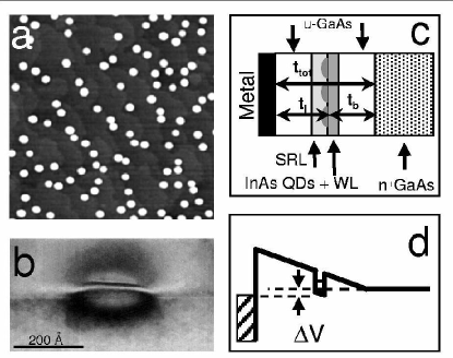
The Schottky diodes were processed over different portions of the wafers, using standard lithography with AuGeNi ohmic back contacts and 1 mm diameter Cr top Schottky gates.
III g-factor assessment
Insofar as spintronics applications are concerned, a key parameter for spin manipulation is the g-factor. The g-factor of a QD determines the radio frequency at which the spin of the electron trapped in the dots would respond for a given static magnetic field. The electron g-factor was evaluated using capacitance spectroscopy, which provides direct information on the QD density of states (DOS).
The capacitance experiments were performed in a 15 T magnet at 2.2 K with lock-in amplifiers at frequencies ranging from 1 kHz to 10 kHz, and an ac amplitude of 4 mVrms superimposed on a varying dc bias. The magnetic field was oriented parallel to the growth direction [001], unless otherwise noticed. The signal/noise ratio for these experiments was always above 105.
The contribution of the structure geometry in the measured capacitance can be easily determined. By solving the Poisson equation for this structure within the depletion approximation, and neglecting the contribution of the QDs, we have:
| (1) |
with ttot as the structure total thickness, and the dielectric constant and relative permissivity of vacuum and medium, the sample area, the electronic charge, the back contact doping concentration, the Schottky barrier height, and the applied bias. This equation takes into account depletion region effects in the back contact, which can be neglected if the doping level is very high. All the capacitance traces for high reverse biases were adjusted in order to obtain the sample area and the doping concentration. The Schottky barrier height was obtained from the flat band voltage as well as from current-voltage characteristics obtained for similar devices. The doping levels and sample area agreed to within 5% of the nominal and measured values. In the approximation of metallic contacts, the relation for the variation of the chemical potential inside the QDs is , with the ratio as the lever arm ratio. If one includes the depletion region effects on the back contact, is given by:
| (2) |
It is important to note that this apparently small correction will produce significant errors if the values for the doping levels as determined by the fits of the capacitance data to equation (1) are not used.
It has been demonstrated that InAs QDs can be modeled quite accurately utilizing a lateral parabolic confinement approximation 16 , for which the eigen-energies are known as a function of an external magnetic field 17 . Including the effect of the applied bias, the Coulomb charge interaction between carriers sequentially added to the QD ensemble, and the Zeeman splitting, the energies of states with one and two electrons in the s shell are 2 :
| (3) |
and
| (4) |
where is the vertical confining potential, the lateral confining potential characteristic energy, the cyclotron frequency, the g-factor modulus, the Bohr’s magneton, the magnetic field intensity, the Coulomb charging energy for the two electrons in the QD ground state, and () the QD chemical potential at which the first (second) electron tunnel into the ground state. One can relate and with the applied bias through equation (2).
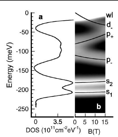
For the other shells one can easily expand the above expressions utilizing the Fock-Darwin eigen-energies. Figure 2 shows capacitance spectra with the background removed after fitting the CV characteristics at large reverse bias with equation (1) for sample A. Figure 2a shows the capacitance spectrum at zero magnetic field. Figure 2b shows a grayscale map of the DOS dependence on the magnetic field, where white means maximal density of states (about cm-2eV-1) and black zero. The calculated electronic spectra dependence on the applied magnetic field given by equation (3) and its extensions to higher angular momentum states (p+, p-, d) are shown. WL denotes the wetting layer level with its corresponding diamagnetic shift.
The voltage at which the first electron will tunnel into the QDs can be found by = , () being the total energy of the system with no (one) electrons. For simplicity, we can make . The voltage for the second electron tunneling event can be found in a similar fashion by equating to . From equations (3) and (4) and the above conditions, by measuring the voltage difference from one to two electrons and utilizing equation (2), we have:
| (5) |
From the dependence of on the magnetic field, one can therefore obtain the g-factor modulus. Figure 3a shows the DOS for s1 and s2 for 0, 7.5 T and 15 T for sample A. The peak spacing is equal to for = 0. Figure 3b the spin splitting dependence on the magnetic field, obtained from for several fields and samples A and D. The g-factor modulus can be found from the slopes of those curves and were and for samples A and D.
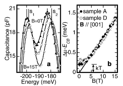
At low magnetic fields one can observe that the linear dependence for the spin splitting disappears. This is a consequence of the thermal energy being roughly the same as the spin-splitting energy for these low magnetic fields (i.e, ). For low fields, capacitance spectroscopy probes quantum levels that can be occupied by either spin orientation. For , the spin of the electrons in the QDs becomes polarized and consequently a linear relationship follows.
IV g-factor tuning and engineering
The basic principle behind g-factor engineering and control lies on the ability of either tailoring the barriers of a given quantum system with different g-factor materials, and/or simultaneously swaying the wave function in and out of the barriers. This comes about from the fact that the effective g-factor of an electron or hole is
| (6) |
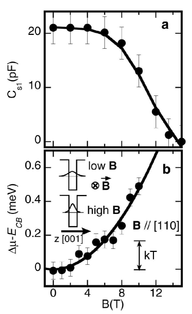
with and the g-factors of the well material (A) and barrier material (B). Therefore if one decreases the wave function penetration inside a barrier the g-factor will change. This was experimentally demonstrated by either applying an electric field parallel to the growth direction 11 ; 12 or a magnetic field perpendicular to the growth direction 3 . For our structures, the signature of a decrease of the tail of back contact and QD wave functions (, ) is a decrease of the capacitive signal of electrons trapped in the s1 state on the magnetic field applied in the [110] direction. As expected, for stronger magnetic fields the signal decreases (See Fig. 4a), indicating a compression of the electron wave functions and into the QD and back contact. Figure 4b shows the capacitance peak spacing excluding () as a function of the magnetic field, exhibiting the non-linear dependence of the spin-splitting and hence the g-factor change. The thermal energy is also represented, indicating that for magnetic fields as high as 6 T, the spin splitting is not clearly visible. Therefore, one can infer a g-factor smaller than 0.5, which increases at stronger magnetic fields. This represents the squeezing of the electron wave function into QDs, thereby altering its in-plane g-factor component.
| Sample | (eV)/ (meV) | (meV) | (meV) | g [001] |
|---|---|---|---|---|
| A | 1.039/41.7 | 44 1 | 25 1 | 1.53 0.03 |
| B | 1.025/48.8 | 46 1 | 20 1 | 1.64 0.02 |
| C | 1.030/33.3 | 49 1 | 20 1 | 1.69 0.02 |
| D | 1.070/34.4 | 46 2 | 18 1 | 1.50 0.04 |
Samples B and C were grown with different capping layers, which according to equation (6) should change the g-factor. Figure 5 and Table 1 summarizes the main results of this paper. Figure 5a shows the grayscale maps for the level dispersion for all samples. The Fock-Darwin levels can be seen quite easily. From the s states, the characteristic energies and Coulomb Blockade can be extracted. Those will influence the g-factor, as they are related to the extent of the wave function. The Coulomb Energy can be evaluated in two ways: a) by measuring the energy difference between states s1 and s2, and b) from , the characteristic length of the wave function can be extracted as , and from that ). These two different approaches agreed within 5% for all samples but sample D, supporting the parabolic confining potential assumption. For sample D, a minor deviation of the parabolic confining potential is observed, as the s-p-d level spacing is different from the values obtained independently for each level dispersion with the magnetic field (Fock-Darwin states). The presence of the d state at zero magnetic field is a clear evidence of that. This reflects a larger size, and can be verified as well by noting that the Coulomb charging energies for sample A is larger than for sample D. Nevertheless, the value for is about the same, meaning that although the islands are different, the trapping potential for the s state is the same.
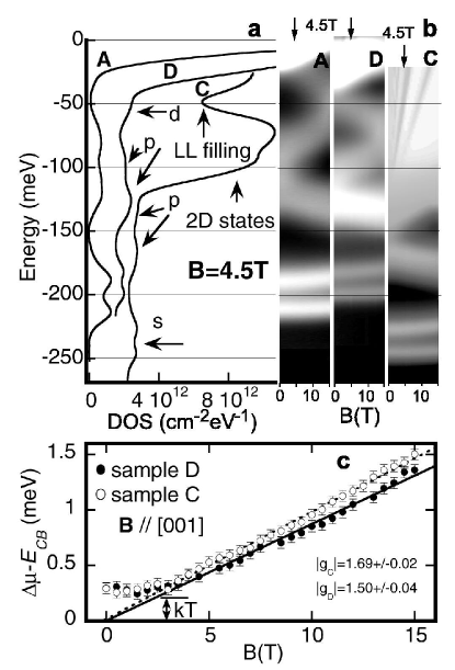
From equation (5), the g-factor for all samples was determined, as shown on Table 1. Samples A and D exhibited the same g-factor, within the experimental uncertainties. This is an extremely important result, evidencing the reproducibility of the procedure for the growth runs, sample processing and measurement. In addition, differences in island shape were not sufficient to change the g-factor. In contrast, the effect of the SRL on the electronic properties and on the g-factor of samples B and C is quite significant. The QD size does not change appreciably, upon contrasting the energies and Coulomb charging energies for all samples. The association of the wetting layer with the SRL producing a thicker quantum well will lower the energy for loading the corresponding 2D levels. A structure revealing the loading of the Landau levels associated with the quantum well can be seen by the dark straight lines on the capacitance spectra. This quantum well prevents the observation of the d levels for both samples, as they were always resonant with the 2D states and therefore not accessible in this experiment. From the data presented here, one can infer that the g-factor is connected to the characteristics of the quantum well, in accord with equation 6. The g factor obtained for samples B and C is systematically larger than for samples A and D (up to 13%). The differences for the g-factor for samples B and C is about 5%, which is experimentally accessible, however the precise details for the differences in the quantum wells for the two samples remain to be further investigated.
V Conclusions
The g-factor control and engineering proposed in this work have an important impact in quantum information processing devices. It was demonstrated that capacitance spectroscopy could be used to measure g-factor of electrons trapped in the ground state of quantum dots. The s-state level of the QDs revealed a robust character insofar as the g-factor was concerned - QDs engineered with small shape differences produced the same g-factor for the electrons on the s shell. This important result addresses the issue of inhomogeneous broadening of the size distribution of quantum dots and g-factor fluctuations - it might not be as severe as one would anticipate. This contrasted with structures with a capping strain reducing layer (SRL), intended to modify the g-factor. By utilizing SRL structures as thin as 3 nm, up to a 13% difference was engineered on the g-factor. A wider range of g-factors can be engineered for QDs, by varying the alloy composition and thickness of the SRL and/or adding materials with different g-factor sign (AlAs, for instance). The control of the g-factor by an external applied magnetic field is yet another handle to be explored. In summary, the g-factor engineering and control for single electrons were demonstrated and represent a key step for solid state quantum information processing devices based on QDs.
Acknowledgments. This work was funded by CNPq, FAPESP and HP Brazil. G.M.R wishes to acknowledge the TEM image by D. Leonard, the use of the high-field magnet at the GPO group at the IFGW, UNICAMP, the IFSC/USP for the access to the MBE apparatus, and the technical support with the MBE by H. Arakaki, C. A. de Souza and E. Marega.
References
- (1) D. P. DiVicenzo: e-print quant-ph 0002077.
- (2) G. Medeiros-Ribeiro, F. G. Pikus, P. M. Petroff, A. L. Efros: Phys. Rev. B 55, 1568 (1997).
- (3) G. Medeiros-Ribeiro, M. V. B. Pinheiro, V. L. Pimentel, E. Marega: Appl. Phys. Lett. 80, 4229 (2002).
- (4) A. Abragam: Electron Paramagnetic Resonance of Transition Ions (Clarendon Press, Oxford 1970).
- (5) M. Bayer, A. Kuther, A. Forchel, A. Gorburov, V. B. Timofeev, F. Schäfer, J. P. Reithmaier, T. L. Reinecke, S. N. Walck: Phys. Rev. Lett. 82, 1748 (1999).
- (6) A. R. Goñi, H. Born, R. Heitz, A. Hoffman, C. Thomsen. F. Heinrichsdorff, D. Bimberg: Jpn. J. Appl. Phys. 39, 3907 (2000).
- (7) J. G. Tischler, A. S. Bracker, D. Gammon, D. Park: Phys. Rev. B 66, 081310 (2002).
- (8) S. Lindemann, T. Ihn, T. Heinzel, W. Zwerger, K. Ensslin, K. Maranowski, A. C. Gossard: Phys. Rev. B 66, 195314 (2002).
- (9) J. R. Petta, D. C. Ralph: Phys. Rev. Lett. 89, 156802 (2002).
- (10) C. Durkan, M. E. Welland: Appl. Phys. Lett. 80, 458 (2002).
- (11) G. Salis, Y. Kato, K. Ensslin, D. C. Driscoll, A. C. Gossard, J. Levy, D. D. Awschalom: Nature 414, 619 (2001).
- (12) Y. Kato, R. C. Myers, D. C. Driscoll, A. C. Gossard, J. Levy, D. D. Awschalom: Science 299, 1201 (2003).
- (13) H. Kosaka, A. A. Kiselev, F. A. Baron, K. W. Kim, E. Yablonovitch: Electronics Letters 37, 464 (2001).
- (14) A. A. Kiselev, K. W. Kim, E. Yablonovitch: Appl. Phys. Lett. 80, 2857 (2002).
- (15) K. Nishi, H. Saito, S. Sugou, J.-S. Lee: Appl. Phys. Lett. 74, 1111 (1999).
- (16) M. Fricke, A. Lorke, J. P. Kotthaus, G. Medeiros-Ribeiro, P. M. Petroff: Europhys. Lett. 36, 197 (1996); R. J. Warburton, C. S. Durr, K. Karrai, J. P. Kotthaus, G. Medeiros-Ribeiro, P. M. Petroff: Phys. Rev. Lett. 79, 5282 (1997); P. Hawrilak, G. A. Narvaez, M. Bayer, A. Forchel, Phys. Rev. Lett. 85, 389 (2000).
- (17) V. Fock: Z. Phys. 47, 446 (1928).