[
Fabrication and Electrical Properties of Pure VO2 Phase Films
Abstract
We have grown VO2 thin films by laser ablation for electronic
device applications. In obtaining the thin films of the pure
VO2 phase, oxygen partial pressure is a critical parameter
because vanadium oxides have several phases with differing oxygen
concentration. It is found that pure VO2 films are
epitaxially grown on -Al2O3 substrate in the
narrow ranges of 55-60 mTorr in an Ar + 10% O2 ambient, and
that mixed phase films are synthesized when the deposition
pressure slightly deviates from the optimum pressure. The (100)
oriented VO2 films undergo an abrupt metal-insulator
transition (MIT) with resistance change of an order of 104 at
338 K. In the films of mixed phases, the small change of the
resistance is observed at the same temperature. The
polycrystalline films grown on SiO2/Si substrate undergo
broaden change of the resistance. Furthermore, the abrupt MIT and
collective current motion appearing in metal are observed when the
electric field is applied to the film.
]
I Introduction
Oxides of vanadium undergo a metal-insulator transition (MIT) at a critical temperature.[1, 2, 3] Among these oxides, vanadium dioxide VO2 has been attracted much attention because its transition temperature is near room temperature, 340 K.[4, 5] The electrical-resistivity change of an order of 104- and the abrupt infrared-transmission change are observed at the transition temperature, which makes it useful for application to electrical and optical switching devices.[6, 7]
The properties of the phase transition of VO2 films strongly depends on the nature of the crystal structure and their stoichiometry, including the film orientation, oxygen content, and residual interface strain. In particular, the oxygen partial pressure is very sensitive in growing the films with a pure VO2 phase. Thus, it is important and necessary, although not easy, to obtain pure phase films for better properties of metal-insulator transition.
To date, there have been various methods used for the successful deposition of VO2 thin films, such as chemical vapor deposition,[8] reactive sputtering,[9] and laser ablation.[5, 6] Pulsed laser deposition was proven to be an excellent method, especially in growing oxide thin films.
In this paper, we deposit (100) oriented VO2 thin films on sapphire substrate by laser ablation, with varying the oxygen partial pressure. The polycrystalline films are grown on the SiO2/Si substrate; detailed properties will be presented in another paper. Phases of the vanadium oxide films are extensively investigated by means of observations of crystal structure and of the resistance change with temperature. Furthermore, metal-insulator transition induced by the electric field is observed.
II Experiments
The VO2 thin films were successfully grown on -Al2O3 (012) and SiO2/Si substrates by laser ablation with a vanadium metal target in an ambient of a partially filled oxygen and argon. The KrF excimer laser (Lambda-Physik, Compex 205) with a wavelength of 248 nm was used to ablate the rotating metal target. An energy density of 12 J/cm2 was focused on the target surface at a repetition rate of 5 Hz. The distance between the target and the substrate was 5 cm. The detailed conditions for the preparation of the vanadium oxide films are described in Table 1. Prior to deposition, the substrates were cleaned with a formal process to remove residual contaminants on their surfaces. The chamber was evacuated down to the base pressure as low as 10-6 Torr. Argon and oxygen gases were filled by adjusting the gas-flow meter. The substrate temperature was kept at 450 ∘C during the deposition process. The film growth was carried out at a pressure between 50 and 200 mTorr. The target was pre-ablated with a shutter for the several minutes to clean the target surface. The partial pressure of oxygen was the most critical variable in obtaining the pure VO2 phase, which was controlled by the working pressure containing 10% oxygen in an argon atmosphere. The deposition rate of VO2 films was estimated to be about 0.39 Å/sec. After deposition, the substrates were slowly cooled to the room temperature under the same deposition atmosphere as that used for growth.
The crystalline structure of deposited films was analyzed by X-ray diffraction (XRD)and high energy electron diffraction (RHEED). The surface morphology and the film composition were observed by scanning electron microscopy (SEM) and secondary ion mass spectrometry (SIMS), respectively. The resistivity of the films was measured using four-probe method. To observe the metal-insulator transition with respect to the electric field, the Au/Cr electrodes were patterned on VO2 thin films by the lift-off method.
III Results and Discussion
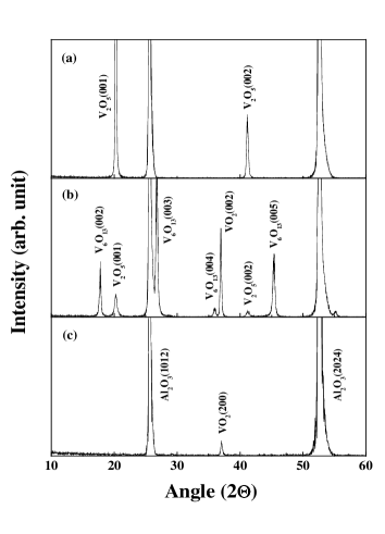
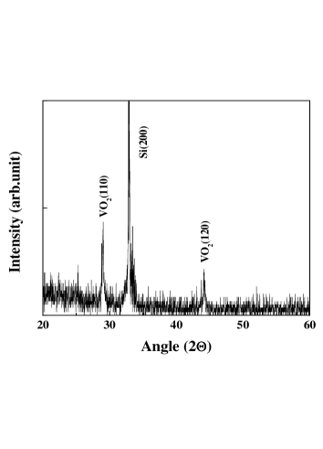
Figure 1 shows X-ray diffraction (XRD) patterns of vanadium oxide films deposited on -Al2O3 (012) substrates in different ambient pressures. The film orientation strongly depends upon partial oxygen contents in the deposition ambient. Although vanadium oxides have several phases, no peaks of phases exist other than those of three phases VO2, V6O13, and V2O5. Figure 1(a) shows that the film synthesized in a pressure of more than about 120 mTorr, is highly (00l) oriented to V2O5. The film deposited in 70 mTorr has mixed phases of VO2, V6O13, and V2O5, as shown in Fig. 1(b). In particular, the (00l) peaks of V6O13 phase were distinct. Figure 1 (c) shows only one peak corresponding to the (200) peak of the monoclinic phase, which indicates the highly preferred orientation of the film. This is in agreement with the results reported by other groups.[5, 6] Thus, VO2 films are grown only in ambient pressures in the range of 55-60 mTorr. Figure 2 shows an XRD pattern of VO2 thin film grown on SiO2/Si substrates. The film was deposited in the same growth conditions on sapphire except for at the deposition temperature of 460 ∘C. The VO2 phase peaks are formed, which means that the VO2 film could be grown even on amorphous SiO2.
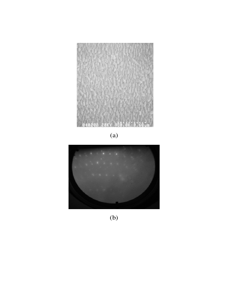
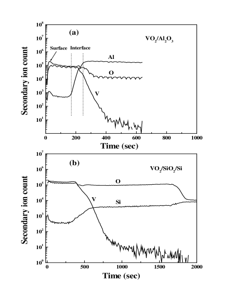
Figure 3 shows the SEM image and the RHEED pattern of the VO2 thin films grown on sapphire substrates. As shown in Fig 3(a), the film surface are formed smoothly with no particulate and grains are densely packed. The average grain size of the film is about 60 nm. A typical RHEED pattern for the VO2 film is appeared in Fig 3(b). The pattern was obtained with an electron energy of 15 keV at a room temperature. The arranged spots are observed although the streaks and Kikuchi lines related to uniform crystal surface are not appeared. The spotted pattern is formed when the films have single crystal structure. Therefore the VO2 thin films on sapphire were grown epitaxial. Figure 4 shows SIMS results of VO2 samples. The element distribution along a depth of the film from a surface is plotted. Vanadium ion for both films grown on sapphire and SiO2/Si substrates deeply penetrates into the substrate. The interface region is largely formed. Silicon ion also diffuses into the VO2 film in Fig. 5(b). This large interdiffusion of elements at the interface may be an obstacle to the growth of pure phase films.
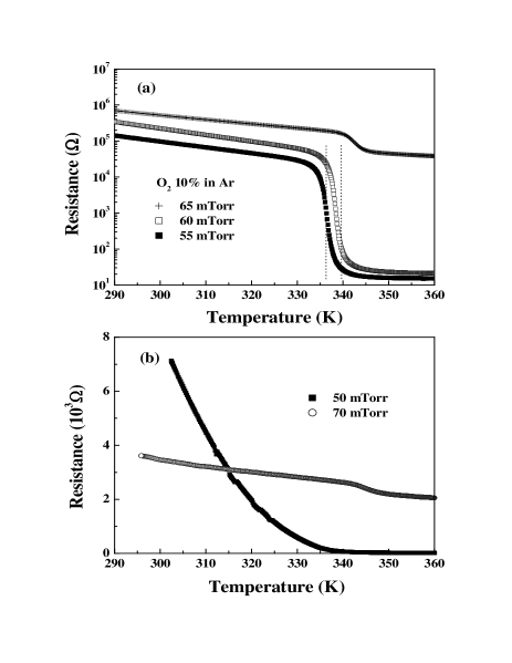
Figure 5(a) shows the temperature dependence of the electrical resistance for vanadium oxide films grown on sapphire in the range of 50-70 mTorr as a function of temperature. The resistance measurement was carried out in a cryostat where the samples are cooled and heated by liquid nitrogen and a heating source. The films grown at 55 and 60 mTorr show abrupt resistance change of in the order of 3104 near a critical temperature, 338 K, which is a structural MIT[1, 2]. This abrupt change with a transition width of about 3 K is comparable to that measured in VO2 single crystal. The electrical resistance below exponentially increases with a decreasing temperature of the film, which is a typical characteristic of semiconductor. The resistance change near for the film grown at the ambient pressure of 65 mTorr is smaller than others.
Figure 5(b) shows that, in a film deposited at 70 mTorr, the resistance change both below and near is much smaller. This property may be attributed to the existence of the mixed phases in the films. Moreover, a film grown at 50 mTorr shows no distinct transition although the film has VO2 phase from x-ray analysis. This may be considered due to the oxygen deficiencies generated during the deposition with a low oxygen partial pressure. As a result of our experiments, it is found that the pure VO2 thin films are obtained at the narrow process window within the range of 5-10 mTorr. It should be noted that the control of the oxygen content during the deposition is most important.
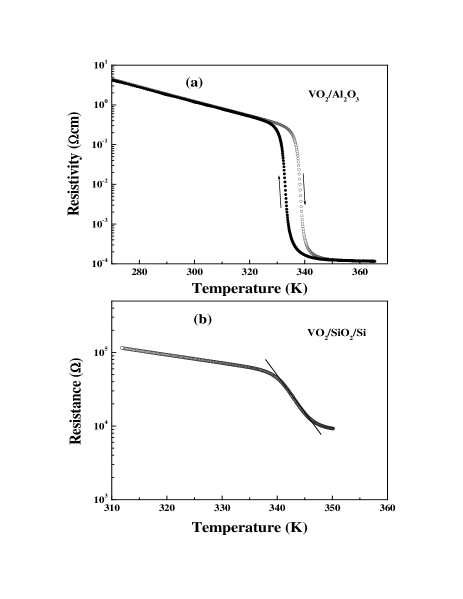
Figure 6 (a) shows the hysteresis of the resistivity measured by increasing and decreasing the temperature. This thermal hysteresis is evidence of the abrupt first-order phase transition. The width of hysteresis is estimated to be about 4 K. Figure 6 (b) shows the temperature dependence of the electrical resistance for the VO2 film deposited on SiO2/Si. It undergoes a metal-insulator transition near 341 K, which indicates formation of the VO2 phase. There is no abrupt change of resistivity of the VO2 films compared with the VO2/Al2O3 films, but the resistance exponentially decreases with an increasing temperature from 340 K and has a transition width of 10 K. These characteristics are resulted from that the film is polycrystalline, as shown in the XRD pattern of Fig. 2.
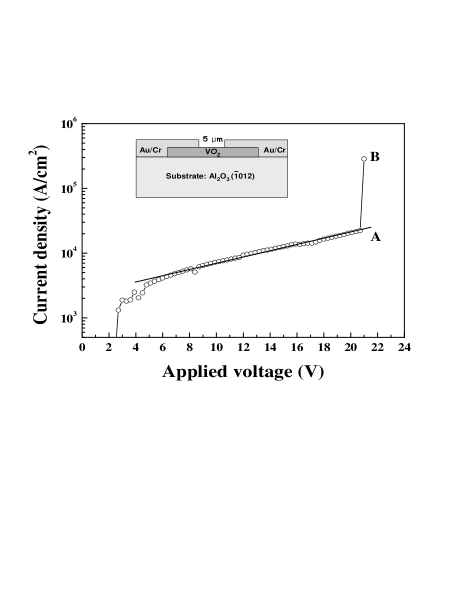
Figure 7 shows the MIT induced by the electric field in a VO2 film grown on sapphire substrate. The schematic diagram of a two terminal structure is displayed in the inset figure. The Au/Cr electrodes to apply the electric field was prepared using the rf-sputtering technique, and patterned into a length of 5 m and a width of 25 m by the lift-off method. The experiment was conducted at room temperature and the maximum current in the instrumentation was limited to prevent the film from damage suffered from a large current flow in advance; the current compliance was 5 mA. The current density increases with an increasing applied voltage below point in Fig. 7. At the indicated point , an abrupt jump is shown; this has been reproducibly observed, and is not interpreted as dielectric breakdown.[10, 11] At point , the current density is about 3 105 A/cm2; this order is given due to compliance, if there is no compliance, the current density is larger than this value. This is regarded as collective current motion appearing in metal. Thus, the jump is the abrupt MIT. The mechanism of the jump is given in a previous paper[12] because it is outside the scope of this paper.
IV Conclusions
We successfully deposited pure VO2 thin films on the sapphire by laser ablation. The working pressure to obtain the pure VO2 phase is near 60 mTorr in an ambient of Ar + 10% O2. The VO2 films on sapphire underwent an abrupt MIT at =338 K with resistance change of an order of 104. The MIT and the collective current motion are observed when the electric field is applied to the film.
REFERENCES
- [1] F. Morin: Phys. Rev. Lett. 3 (1959) 34.
- [2] D. B. McWhan, T. M. Rice, and J. P. Remeika: Phys. Rev. Lett. 23 (1969) 1384.
- [3] S. Shin, S. Suga, M. Taniguchi, M. Fujisawa, H. Kanzaki, A. Fujimori, H. Daimon, Y. Ueda, K. Kosuge, and S. Kachi: Phys. Rev. B 41 (1990) 4993.
- [4] D. P. Partlow, S. R. Gurkovich, K. C. Radford, and L. J. Denes: J. Appl. Phys. 70 (1991) 443.
- [5] Mark Borek, F. Qian, V. Nagabushnam, and R. K. Singh: Appl. Phys. Lett. 63 (1993) 3288.
- [6] Y. Muraoka and Z. Hiroi: Appl. Phys. Lett. 80 (2002) 583.
- [7] D. H. Kim and H. S. Kwok: Appl. Phys. Lett. 65 (1994) 3188.
- [8] H. K. Kim, H. You, R. P. Chiarello, H. L. M. Chang, T. J. Zhang, and D. J. Lam: Phys. Rev. B 47 (1993) 12900.
- [9] P. Jin, K. Yoshimura, and S. Tanemura: J. Vac. Sci. Technol A 15 (1997) 1113.
- [10] P. P. Boriskov, A. A. Velichko, A. L. Pergament, G. B. Stefanovich, and D. G. Stefanovich: Tech. Phys. Lett. 28 (2002) 406.
- [11] R. Kumai, Y. Okimoto, and Y. Tokura: Science 284 (1999) 1645.
- [12] H. T. Kim, B. G. Chae, D. H. Youn, S. Y. Maeng, and K. Y. Kang: cond-mat/0305632.
| Atomsphere | Ar + O210% |
|---|---|
| Laser power | 200 mJ |
| Repetition rate | 5 Hz |
| Target | V metal target |
| Substrate | -Al2O3 (012)and SiO2/Si |
| Initial pressure | below 10-6 Torr |
| Deposition pressure | 50200 mTorr |
| Substrate-target distance | 5 cm |