Snell’s law for surface electrons: Refraction of an electron gas imaged in real space
Abstract
On NaCl(100)/Cu(111) an interface state band is observed that descends from the surface-state band of the clean copper surface. This band exhibits a Moiré-pattern-induced one-dimensional band gap, which is accompanied by strong standing-wave patterns, as revealed in low-temperature scanning tunneling microscopy images. At NaCl island step edges, one can directly see the refraction of these standing waves, which obey Snell’s refraction law.
pacs:
68.37.Ef, 73.20.At, 73.61.NgEver since the mapping of standing waves of a two-dimensional electron gas (2DEG) on the close-packed Cu(111) surface by means of low-temperature scanning tunneling microscopy (LT-STM) Crommie93 ; Hasegawa93 , the 2DEG turned out to be an ideal playground for a variety of LT-STM experiments Buergi98 ; Ji03 ; Manoharan01 ; Kliewer01a ; Suzuki01 ; Bendounan03 ; Diekhoener03 ; Kliewer01b ; Park00 ; Repp00 . In the STM images the surface electrons reveal their wave-like behavior, often discussed in analogy to light. This analogy has been addressed directly in experiments such as the confinement of a 2DEG between two parallel step edges, considered as a counterpart of the optical Fabry-Perot resonator Buergi98 , the striking experiment of an electronic Mach-Zehnder interferometer Ji03 , and the spectacular quantum mirage experiment Manoharan01 . However, despite this strong analogy, the counterpart of optical refraction has not yet been observed for surface electrons.
Such an experiment has to comply with several requirements. First of all, two different media are necessary. For surface electronic states, two regions having different dispersions may act as the media and be realized by a partial coverage of the surface with an adlayer that modifies the dispersion, as was observed for various thin metal films on Cu(111) Kliewer01a ; Suzuki01 ; Bendounan03 ; Diekhoener03 as well as for Xe/Cu(111) Park00 . Second—in terms of optics—the interface between the two media has to be transparent. It was reported that step edges of metals exhibit a transmission close to zero for surface electrons, i.e., that the wave patterns on the two sides of a step edge are not related to each other Buergi98 . However, in the case of an insulator adsorbed on a metal surface, this may be different: An insulator does not contribute to the electronic states, therefore the electrons are still confined to the surface of the metal underneath, and thus may better overlap with the electrons of the clean surface. Third, in addition to being inherently transparent, the interface between the two media also has to be very smooth. This means that a perfect step edge is needed to observe refraction of surface electrons.
As NaCl/Cu(111) meets the above requirements, we are able to report here the first observation of the refraction of surface electronic waves at island step edges by means of LT-STM. Moreover, we show that natural Moiré patterns, inherent in incommensurate growth, generate a band gap within a two-dimensional (2D) interface state band. Thereby the textbook band-structure model of nearly free electrons (NFE) is exploited and visualized in real space.
Our experiments were performed with a LT-STM Meyer96 operated at 9 K. The sample was cleaned by several sputtering and annealing cycles. NaCl was evaporated thermally, while the sample temperature was kept at 320 K. Bias voltages refer to the sample voltage with respect to the tip, and we used electrochemically etched tungsten wire as STM tips.
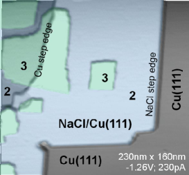
NaCl forms (100)-terminated islands that are up to several microns in diameter Bennewitz99 (see Fig. 1). The NaCl islands start with a double-layer thickness and perfect nonpolar step edges, in which the anions and the cations alternate. On top of the initial double layer, islands of additional layers are formed. Substrate defect steps are smoothly overgrown in the so-called carpet-like growth Schwennicke93 . Because of the different symmetries of NaCl(100) and Cu(111), the growth is incommensurate. In the case of only a few layers of NaCl, the nonvanishing tail of charge density from the metal that extends through the insulator is sufficient to take STM images without crashing the tip. In atomically resolved STM images, only the Cl ions are imaged as protrusions Hebenstreit99 ; Repp01 ; Olsson .
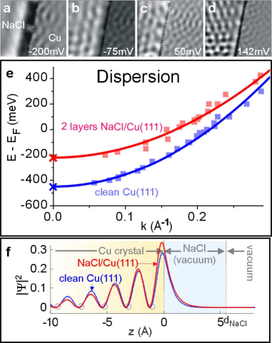
Upon adsorption of NaCl, the Cu(111) surface state band survives and forms an interface state band that is confined to the insulator/metal interface and has a larger Fermi wavelength of nm (clean Cu: nm). To measure the dispersion of this modified 2D interface state band, differential conductance (d/d) images were taken at various bias voltages, as shown in Figs. 2(a)-(d). By extracting the wavelength of the wave patterns seen in these images constantcurrent , the dispersion relation can be established (see Fig. 2(e)), as was done for the clean Cu surface Crommie93 ; Hasegawa93 ; Horm94 . The band minimum was obtained by recording the d/d signal at a fixed position as a function of energy Horm94 ; Li98 (crosses in Fig. 2(e)) and is shifted upward in energy by meV in the case of the adsorption of an insulating NaCl overlayer. The resulting parabolic dispersion is slightly wider, i.e., the effective mass has increased from to , where denotes the free electron mass.
The energy shift can be qualitatively understood within the one-dimensional (1D) phase-accumulation model Smith85 ; Hotzel99 . In this analysis, the wave function of surface electrons is found by matching the wave-function phase of the analytical solution inside the copper crystal Forstmann70 to the one of the numerical solution for the outside region, obtained by integrating the Schrödinger equation Smith85 . For the latter an electrostatic potential had to be assumed: For the clean Cu surface, this is given by the image potential potential . For NaCl/Cu(111) we considered the modified image potential Hotzel99 ; potential as well as the lowering of the work function upon NaCl adsorption Bennewitz99 .
This model yields an upward shift of the dispersion of meV, in qualitative agreement with our experiment. Even more relevant, it reveals that the wave functions of the surface electrons are barely modified upon adsorption of NaCl (see Fig. 2(f)) and thus render a high transmission through NaCl step edges promising. Moreover, it justifies an even simpler understanding of the upward shift in the dispersion within first-order perturbation theory, . Owing to the exponentially decaying wave function outside the Cu substrate, the perturbation potential , i.e., the potential difference with and without NaCl, is only relevant for the energy shift in immediate proximity of the copper surface. The upward shift thus results from the positive perturbation potential at the interface given by the weaker image potential potential due to the polarization of the adsorbed dielectric. The work-function change Bennewitz99 as well as the image potential at the insulator-to-vacuum interface are negligible for . Consequently, the dispersion for three layers of NaCl does not differ from that for two layers, which was verified in the experiment.
The above results show that for interface states of an insulator/metal system, as described here, the main contribution of the electronic wavefunctions resides within the substrate (see Fig. 2(f)). Therefore, the effective mass of the shifted interface state will mainly be determined by the metal. For copper an upward shift of the surface state is expected to be correlated with a slight increase of the effective mass as discussed in Ref. Smith85 , in good agreement with the present experiment. The energetic shift of the band for other insulator/metal systems will depend critically on the structure of the interface. However, the adsorption of an insulator that does not strongly affect the metal surface but weaken its image potential will in general result in an upward shift of the surface state band. These findings explain that in a previous experiment on Xe/Cu(111) Park00 a similar upward shift and effective mass increase were observed.
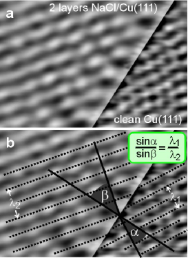
Another condition for the observation of the electron refraction at island edges is the presence of standing waves. Continuous waves lead to a uniform probability distribution and thus prevent the observation of refraction in the STM images, even if the refraction took place. In the case of NaCl/Cu(111), strong electronic plane waves are already inherent in the system: The incommensurate growth gives rise to various Moiré patterns pattern , which can be seen in atomically resolved STM images (Fig. 3(a)). The Moiré patterns will be associated with displacements of the charged ions and are thus accompanied by a modulation of the electrostatic potential seen by the surface electrons. One general conclusion of the NFE model Ashcroft is that any periodic potential modulation will give rise to a band gap. Just below and just above the band gap, the electronic wave functions are expected to be standing waves, and the probability distributions will have a phase shift of with respect to each other, as illustrated in Fig. 3(c). For the case discussed here, this physics textbook statement can be imaged in real space. As a first indication, STM images such as that in Fig. 3(b) show strong standing plane waves that correspond to this particular Moiré pattern in terms of wavelength and direction (dotted lines in Fig. 3(a) and (b)).
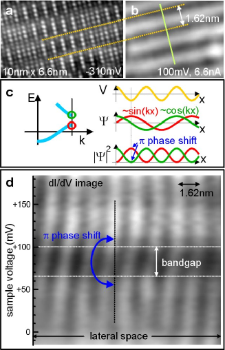
For a more precise analysis, we recorded an d/d image in constant-height mode, but whereas we scanned within one scan line perpendicular to the plane waves (as indicated by the solid line in Fig. 3(b)), we did not move the tip in the other direction. Instead, we changed the bias voltage after each scan line. The resulting STM image in Fig. 3(d) thus reflects a map of the probability distribution in space and energy. As expected, the image shows a region of reduced intensity, which represents the band-gap region. Just above and just below this region, there are strong standing-wave patterns shifted by to each other.
The standing-wave pattern caused by a periodic scattering potential contains only the wavelength components of this potential modulation. Thus in Fig. 3(d), the standing-wave pattern is given by the Moiré pattern’s periodicity and does not change with energy. The position in energy of the band gap can vary between 20 and 400 meV above the Fermi level from one rotational domain to the next. In all cases, this energy position can be linked to the Moiré patterns in such a way that the wave vector at the band gap corresponds to half of the wave vector of the potential modulation, in agreement with the NFE model. In the particular case shown in Fig. 3 the Moiré pattern has a periodicity of nm corresponding to Å-1, Å-1, and thus meV. As this condition is met only in one direction, we have a 1D band gap in a 2D electron gas, i.e., a pseudo gap. For some rotational domains, the condition was not met in the experimentally accessible energy range, and no band gap was observed, as in the case of the dispersion shown in Fig. 2(e).
The standing-wave pattern persists far above the band gap because of the one-dimensionality of the band gap. This is also one of the reasons for the remaining low intensity within the band gap. In addition, the finite lifetime of the interface states Kliewer01b gives rise to an energetic broadening of the states, which further “smears out” the bandgap and may also lead to interference effects.
To observe the refraction, we took advantage of the strong standing plane waves just below the band gap by applying a corresponding bias voltage of meV. Figure 4 shows the refraction of the surface electrons in a differential conductance (d/d) image of an island edge of NaCl/Cu(111). The region on the NaCl island (to the left) shows a strong standing plane-wave pattern that is due to the formation of a band gap. Reflection induces an additional modulation of the pattern parallel to the step edge. More importantly, the image clearly reveals standing plane waves on the clean copper surface (to the right). These patterns at the island step edge obey Snell’s refraction law, . Note that and are given by the geometry of this particular Moiré pattern, is the electron wavelength on the clean Cu surface corresponding to meV, and is given by Snell’s law. This law follows directly from the conservation of the component of the momentum (and wavelength) parallel to the step. In other words, the patterns on both sides have a fixed phase correlation at the step edge, which is directly evident in the images and follows from the postulation of continuous wave functions in quantum mechanics.
In everyday life, optical refraction manifests itself in the bending of light rays, and we cannot observe the wave fronts directly. In Fig. 4 we do not observe the bending of rays, but directly image the wave fronts, visualizing the refraction model. Another difference to optics is evident: In optics the refraction is usually determined by one term only, namely, the refractive index of the medium. In the case of electron refraction, the band minimum as well as the effective mass of the electrons may change and thus contribute to the refraction in different ways.
The observed band-gap formation due to Moiré patterns is similar to the superlattice concept Esaki70 ; Dingle75 based on the idea of creating artificial, tunable 1D band gaps by growing a vertical lattice of alternating semiconductors. Whereas in semiconductor superlattices the band gaps can be tuned by the layer thicknesses during growth, Moiré-pattern-induced band gaps can be tuned by the choice of lattice constant mismatch. This phenomenon shows a new way to tailor the properties of a 2DEG for future applications. These possibilities can be further extended by controlled sequential growth of different dielectric materials. In contrast to surface states, interface states are inherently protected by the dielectric adlayer and can even be studied under ambient conditions.
In summary, we observed the formation of a 1D band gap in the 2D electron gas of the NaCl/Cu(111) interface state band. The band gap is due to the Moiré patterns of the incommensurate growth and was observed in an STM image displaying the electron-probability distribution in space and energy. At NaCl island edges, the refraction of standing waves could be observed, obeying Snell’s refraction law.
Acknowledgements.
We thank Frank Forstmann and Rolf Allenspach for fruitful discussions, and acknowledge partial funding by the EU-TMR projects “AMMIST” and “NANOSPECTRA” and the Deutsche Forschungsgemeinschaft Project No. RI 472/3-2.References
- (1) M. F. Crommie, C. P. Lutz, and D. M. Eigler, Nature 363, 524 (1993).
- (2) Y. Hasegawa and Ph. Avouris, Phys. Rev. Lett. 71, 1071 (1993).
- (3) L. Bürgi et al., Phys. Rev. Lett. 81, 5370 (1998).
- (4) Y. Ji et al., Nature 422, 415 (2003).
- (5) H. C. Manoharan, C. P. Lutz, and D. M. Eigler, Nature 403, 512 (2001).
- (6) J. Kliewer and R. Berndt, Appl. Phys. A 72, 155 (2001).
- (7) T. Suzuki et al., Phys. Rev. B 64, 081403(R) (2001).
- (8) A. Bendounan et al., Phys. Rev. B 67, 165412 (2003).
- (9) L. Diekhöner et al., Phys. Rev. Lett. 90, 236801 (2003).
- (10) J.-Y. Park et al., Phys. Rev. B 62, R16341 (2000).
- (11) J. Kliewer et al., Science 288, 1399 (2000).
- (12) J. Repp et al., Phys. Rev. Lett. 85, 2981 (2000).
- (13) G. Meyer, Rev. Sci. Instrum. 67, 2960 (1996).
- (14) R. Bennewitz et al., Surf. Sci. 438, 289 (1999).
- (15) C. Schwennicke, J. Schimmelpfennig, and H. Pfnür, Surf. Sci. 293, 57 (1993).
- (16) W. Hebenstreit et al., Surf. Sci. 424, L321 (1999).
- (17) F. Olsson, M. Persson, J. Repp, and G. Meyer, unpublished.
- (18) J. Repp, S. Fölsch, G. Meyer, and K.-H. Rieder, Phys. Rev. Lett. 86, 252 (2001).
- (19) The d/d images presented in Figs. 4 and 2 are recorded in constant-current mode to enable simultaneous imaging on both sides of the step edge. To determine the dispersion, constant-height images were used as well.
- (20) G. Hörmandinger, Phys. Rev. B 49, 13897 (1994).
- (21) J. Li et al., Phys. Rev. Lett. 81, 4464 (1998).
- (22) N. V. Smith, Phys. Rev. B 32, 3549 (1985).
- (23) A. Hotzel et al., Appl. Phys. B 68, 615 (1999).
- (24) F. Forstmann, Z. Phys. 235, 69 (1970).
- (25) As in Ref. Hotzel99 we treated the image potential classically by applying the static dielectric constant of NaCl. The nonphysical divergence of the image potential was suppressed. The average barrier potential within the NaCl layer is given by the upper edge of the band gap.
- (26) The pattern shown in Fig. 3(a) corresponds to a NaCl lattice constant of Å and a rotational domain in which the polar NaCl direction is almost parallel () to the close-packed direction of the copper substrate. This alignment of the two directions seems favorable, although also other rotational domains exist.
- (27) N. W. Ahscroft and N. D. Mermin, in Solid State Physics, edited by D. G. Crane (Holt, Rinehart and Winston, Orlando, 1976) Ch. 9.
- (28) L. Esaki and R. Tsu, IBM J. Res. Develop. 14, 61 (1970).
- (29) R. Dingle, A. C. Gossard, and W. Wiegmann Phys. Rev. Lett. 34, 1327 (1975).