Tailoring Josephson coupling through superconductivity-induced nonequilibrium
Abstract
The distinctive quasiparticle distribution existing under nonequilibrium in a superconductor-insulator-normal metal-insulator-superconductor (SINIS) mesoscopic line is proposed as a novel tool to control the supercurrent intensity in a long Josephson weak link. We present a description of this system in the framework of the diffusive-limit quasiclassical Green-function theory and take into account the effects of inelastic scattering with arbitrary strength. Supercurrent enhancement and suppression, including a marked transition to a -junction are striking features leading to a fully tunable structure.
pacs:
74.50.+r, 73.23.-b, 74.40.+kNonequilibrium effects in mesoscopic superconducting circuits have been receiving a rekindled attention during the last few years articles . The art of controlling Josephson coupling in superconductor-normal metal-superconductor (SNS) weak links is at present in the spotlight: a recent breakthrough in mesoscopic superconductivity is indeed represented by the SNS transistor, where supercurrent suppression as well as its sign reversal (-transition) were demonstrated baselmans ; baselmansphase . This was achieved by driving the quasiparticle distribution in the weak link far from equilibrium volkov ; wilhelm ; yip through external voltage terminals, viz. normal reservoirs. Such a behavior relies on the two-step shape of the quasiparticle nonequilibrium distribution, typical of diffusive mesoscopic wires and experimentally observed by Pothier and coworkers pothier .
The purpose of this paper is to demonstrate that it is possible to tailor the quasiparticle distribution through superconductivity-induced nonequilibrium in order to implement a unique class of superconducting transistors. This can be achieved when mesoscopic control lines are connected to superconducting reservoirs through tunnel barriers (I), realizing a SINIS channel. The peculiar quasiparticle distribution in the N region, originating from biasing the S terminals, allows one to access several regimes, from supercurrent enhancement with respect to equilibrium to a large amplitude of the -transition passing through a steep supercurrent suppression. These features are accompanied by a large current gain (up to some in the region of larger input impedance) and reduced dissipation. The ultimate operating frequencies available open the way to the exploitation of this scheme for the implementation of ultrafast current amplifiers.
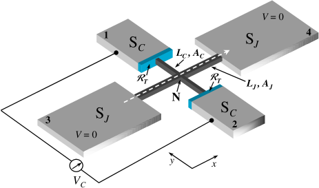
The investigated mesoscopic structure (see Fig. 1) consists of a long diffusive weak link of length much larger than the superconducting coherence length () oriented along the direction. This defines the SNS junction of cross-section . The superconducting terminals belonging to the SNS junction, labelled SJ (3 and 4), are kept at zero potential. The SINIS control line is oriented along the direction and consists of a normal wire, of length and cross-section , connected through identical tunnel junctions of resistance to two superconducting reservoirs SC (1 and 2), biased at opposite voltages . The superconducting gaps of SJ and SC ( and ) are in general different.
The supercurrent flowing across the SNS junction is given by wilhelm ; yip
| (1) |
and depends on the quasiparticle distribution function . In Eq. (1), is the normal-state conductivity which determines the normal-state resistance of the junction according to . The distribution function reduces to the equilibrium Fermi distribution when . The energy-dependent spectral supercurrent belzig ; tero , , can be calculated by solving the Usadel equations usadel . Following the parametrization of the Green functions given in Ref. belzig , these equations in the N region can be written
| (2) |
where is the diffusion coefficient and is the energy relative to the chemical potential in SJ. and are in general complex functions. For perfectly transmissive contacts, the boundary conditions at the SJN interfaces reduce to arctanh and in the reservoirs , where is the phase difference between the superconductors.
As required by Eq. (1) we must determine the actual quasiparticle distribution in the N region of the SINIS structure. This is controlled by voltage () and temperature, and by the amount of inelastic scattering in the control line. In the case of a short control wire with no inelastic interactions, the quasiparticle distribution, according to Ref. Heslinga , is given by
| (3) |
where and . The former are the BCS densities of states in the reservoirs SC (labeled by 1 and 2 in Fig. 1). is the Fermi function at lattice temperature lowenote . In this case Eqs. (1) and (3) yield the dimensionless transistor output characteristics shown in Fig. 2(a). The latter plots the supercurrent versus control bias at different temperatures for a long junction (i.e., , where is the Thouless energy of the SNS junction, as this is the limit where the supercurrent spectrum varies strongly with energy). We assumed , , where are the critical temperatures of the superconductors SC(J) and such that .

At the lowest temperatures, by increasing curves display a large supercurrent enhancement with respect to equilibrium at bias (region I in the figure). Further increase of bias leads to a -transition (region II) and finally to a decay for larger voltages. This behavior is explained in Figs. 2(b,c,d) where the spectral supercurrent (solid line) is plotted together with (dash-dotted line) for values of and corresponding to regions I, II and III, respectively. Hatched areas represent the integral of their product, i.e., the supercurrent of Eq. (1). In particular, region I corresponds to the cooling regime where hot quasiparticles are extracted from the normal metal Heslinga ; leivo . The origin of the -transition in region II is illustrated by Fig. 2(c), where the negative contribution to the integral is shown. We remark that the intensity of the supercurrent inversion is very significant. It reaches about 60 of the maximum value of at in the whole temperature range, nearly doubling the -state value of the supercurrent as compared to the case of an all-normal control channel wilhelm ; yip . In the high-temperature regime (), when the equilibrium critical current is vanishing, the supercurrent first undergoes a low-bias -transition (region III in the figure), then enters regions I and II. This recover of the supercurrent from vanishingly small values at equilibrium is again the consequence of the peculiar shape of (see Fig. 2(d)). Notably, the supercurrent enhancement around remains pronounced even at the highest temperatures, so that attains values largely exceeding 50 of the junction maximum supercurrent. This demonstrates the full tunability of the supercurrent through nonequilibrium effects induced by the superconducting control lines. We remark that this is a unique feature stemming from the superconductivity-induced nonequilibrium population in the weak link.
The length of the SINIS control line can be additionally varied to control the supercurrent by changing the effective strength of inelastic scattering in the N region. For , the distribution function in the N region is essentially -independent and we have
| (4) |
Here is the normal-metal density of states at the Fermi energy, is the volume of the N region and is the net collision rate at energy . At low temperatures, the most relevant scattering mechanism is electron-electron scattering anthore and we can neglect the effect of electron-phonon scattering. Then nag ; pothier ,
| (5) |
and
| (6) | |||
| (7) |
Electron-electron interaction is either due to direct Coulomb scattering AA ; kamenev or mediated by magnetic impurities anthore . Below, we concentrate on the former, but the latter would yield a similar qualitative behavior. From the calculation of the screened Coulomb interaction in the diffusive channel, it follows AA that for a quasi-one dimensional wire and kamenev . We note that is the most relevant energy scale to describe the distribution function for different voltages . It is thus useful to replace and , in order to obtain a dimensionless equation. Multiplying Eq. (4) by we obtain
| (8) |
where , and . In the absence of electron-electron interaction () Eq. (3) is recovered.

The influence of inelastic scattering on is shown in Fig. 3, which displays the critical current of a long junction at for several values of . Here is obtained by numerically solving Eq. (8). The effect of electron-electron interaction is to strongly suppress the -state and to widen the peak around . The -transition vanishes for , but the enhancement due to quasiparticle cooling still persists in the limit of even larger inelastic scattering giazotto . The disappearance of the -state can be understood by looking at the right inset of Fig. 3 which clearly shows how (calculated at ) gradually relaxes from nonequilibrium towards a Fermi function upon increasing . The left inset shows how (evaluated at ) sharpens, thus enhancing , by increasing . This effect follows from the fact that inelastic interactions redistribute the occupation of quasiparticle levels in the N region, thus increasing the occupation at higher energy. As a consequence, higher-energy excitations are more effectively removed by tunneling, even for biases well below and not only around (as in the case of ). At the same time, supercurrent recovery at high temperature is gradually weakened upon enhancing . Notably, these calculations show that a rather large amount of inelastic scattering is necessary to weaken and completely suppress the -state. For example, using Al/Al2O3/Cu as materials composing the SINIS line, corresponds to use a fairly long control line with m device .
Changing the ratio shifts the response along the axis, the shape of the characteristics being virtually independent of . This translates into a different magnitude of control voltages and power dissipation , where is the control current across the SINIS channel. The function is plotted in Fig. 4(a) for some ratios at , assuming and K. The impact of in controlling power dissipation is easily recognized. These effects clearly indicate that is the condition to be fulfilled in order to minimize . In practice, the power dissipation for constitutes an experimental problem as this energy needs to be carried out from the reservoirs. In a similar way the noise properties of the system are sensitive to the different ratios.

Assuming that the noise through one junction is essentially uncorrelated from the noise through the other, it follows that the input noise power in the control line can be expressed as
| (9) |
from Eq. (9) is shown in Fig. 4(b) for the same parameters of Fig. 4(a). For example, for (corresponding roughly to the combination Al/Nb), obtains values of the order of a few W and of some A2Hz-1 in the cooling regime, while these values are enhanced respectively to few tens of W and A2Hz-1 for biases around the -transition.
In light of the possible use of this operational principle for device implementation, let us comment on the available gain and switching times. Input and output voltages are of the order of and , respectively, so that it seems hard to achieve voltage gain. On the other hand, differential current gain can be very large. For a simple estimate gives , meaning that with realistic ratios (), can exceed . calculated for is plotted in Fig. 4(c) (the inset shows the gain in the -state region). This calculation reveals that can reach huge values, with some for gain and several in the opposite regime. Remarkably, gain is almost unchanged also in the presence of weak inelastic scattering (i.e., ). The same holds for and . The highest operating frequency of the transistor is limited by the smallest energy in the system: where is the tunnel junction capacitance. For an optimized device, working frequencies of the order of Hz can be experimentally achieved in the high-voltage regime . For , conversely, the response is slower (somewhat below Hz), owing to the long discharging time through the junctions.
We thank M. H. Devoret, K. K. Likharev, F. Pierre, L. Roschier, A. M. Savin, and V. Semenov for helpful discussions. This work was supported in part by MIUR under the FIRB project RBNE01FSWY and by the EU (RTN-Nanoscale Dynamics).
References
- (1) See, for example, Theory of Nonequilibrium Superconductivity, N.B. Kopnin (Clarendon Press, Oxford, 2001).
- (2) J.J.A. Baselmans, A.F. Morpurgo, B.J. van Wees, and T.M. Klapwijk, Nature (London) 397, 43 (1999); J. Huang, F. Pierre, T.T Heikkilä, F.K. Wilhelm, and N.O. Birge, Phys. Rev. B 66, 020507 (2002); R. Shaikhaidarov, A.F. Volkov, H. Takayanagi, V.T. Petrashov, and P. Delsing, ibid. 62, R14649 (2000).
- (3) J.J.A. Baselmans, T.T. Heikkilä, B.J. van Wees, and T.M. Klapwijk, Phys. Rev. Lett. 89, 207002 (2002).
- (4) A. F. Volkov, Phys. Rev. Lett. 74, 4730 (1995).
- (5) F.K. Wilhelm, G. Schön, and A.D. Zaikin, Phys. Rev. Lett. 81, 1682 (1998).
- (6) S.-K. Yip, Phys. Rev. B 58, 5803 (1998).
- (7) H. Pothier, S. Guéron, N.O. Birge, D. Esteve, and M.H. Devoret, Phys. Rev. Lett. 79, 3490 (1997).
- (8) See W. Belzig, F.K. Wilhelm, C. Bruder, G. Schön, and A.D. Zaikin, Superlattices Microstruct. 25, 1251 (1999) and references therein.
- (9) T.T. Heikkilä, J. Särkkä, and F.K. Wilhelm, Phys. Rev. B 66, 184513 (2002).
- (10) K.D. Usadel, Phys. Rev. Lett 25, 507 (1970).
- (11) D.R. Heslinga, and T.M. Klapwijk, Phys. Rev. B 47, 5157 (1993).
- (12) At low control voltages there is a region of energies where . We assume that there the (otherwise weak) coupling to phonons makes the distributions at those energies equal to the equilibrium Fermi distribution. A more detailed discussion and another type of coupling is given in cooler .
- (13) J.P. Pekola, T.T. Heikkilä, A.M. Savin, J.T. Flyktman, F. Giazotto, and F.W.J. Hekking, submitted.
- (14) M.M. Leivo, J.P. Pekola, and D.V. Averin, Appl. Phys. Lett. 68, 1996 (1996).
- (15) A. Anthore, F. Pierre, H. Pothier, and D. Esteve, Phys. Rev. Lett. 90, 076806 (2003).
- (16) K.E. Nagaev, Phys. Rev. B 52, 4740 (1995).
- (17) B.L. Altshuler and A.G. Aronov, Zh. Eksp. Teor. Fiz. 75, 1610 (1978) [Sov. Phys. JETP 48, 812 (1982)].
- (18) A. Kamenev and A. Andreev, Phys. Rev. B 60, 2218 (1999).
- (19) F. Giazotto, F. Taddei, T.T. Heikkilä, R. Fazio, and F. Beltram, Appl. Phys. Lett. 83, 2877 (2003).
- (20) This is straightforward assuming as typical parameters , m2/s and eV.
- (21) In this calculation we chose to include depairing by a phenomenological, but realistic parameter cooler . Its omission would lead to extremely higher values.