Ion beam sputtering method for progressive
reduction of nanostructures dimensions
Abstract
An ion beam based dry etching method has been developed for progressive reduction of dimensions of prefabricated nanostructures. The method has been successfully applied to aluminum nanowires and aluminum single electron transistors (SET). The method is based on removal of material from the structures when exposed to energetic argon ions and it was shown to be applicable multiple times to the same sample. The electrical measurements and samples imaging in between the sputtering sessions clearly indicated that the dimensions, i.e. cross-section of the nanowires and area of the tunnel junctions in SET, were progressively reduced without noticeable degradation of the sample structure. We were able to reduce the effective diameter of aluminum nanowires from 65 nm down to 30 nm, whereas the tunnel junction area has been reduced by 40 %.
pacs:
74.40.+k, 68.65.La, 73.23.Hk, 61.80.JhI Introduction
There is a variety of different techniques available for fabrication of nano- or micron-sized structures. Ultraviolet (UV) lithography is widely used in microelectronic industry to fabricate large-scale integrated circuits with vast amount of functional elements at once. However, the minimum lateral dimensions attainable with this technique is about 250 nm. By using deep UV light the limit might be pushed close to 100 nm in the futurexia . More advanced methods based on electron beam lithography (EBL) are capable to provide even smaller dimensions and have been applied, e.g., for fabrication of 5-7 nm wide etched lines on a silicon substrateChenAhmed . However, when evaporating metallic structures through masks made with EBL the limit is higher, around 20-50 nm, depending on the molecule size of the resist material and the performance of the particular equipment. The disadvantage of EBL is that it is rather slow. X-rays lithography can in principle be used for patterning, but this method requires significantly more efforts and complicated masksxia . It is also possible to use the sharp tip of an atomic force microscope (AFM) to transfer single particles on a substrate to form a nanopattern lindeli . Alternatively, one can oxidize patterns on the hydrogen-passivated surface with the tip or scratch the pattern on a thin resist layer (see Ref. Anssi, and references therein for detailed description of the AFM based methods). The difficulty in using AFM in patterning is in removal of the mask material (lift-off) after metal evaporation. As a result, at present moment AFM based nanofabrication has rather limited range of applications.
We studied a different kind of approach where the dimensions of the prefabricated nanosized structures are reduced by ion beam sputtering in controllable and reproducible way. We used aluminum nanowires and single electron transistors (SET) to test applicability of the sputtering method. SET is one of the fundamental components in nanoelectronics and ultrasmall tunnel junctions in general have a lot of potential applications in the futurepashkin . The change in the dimensions of the tunnel junctions was detected by electrical measurements of the charging energy at liquid helium temperature 4.2 K. In case of a nanowire, the decrease of the diameter was determined from the width of superconducting transition .
Generally speaking, it is common to study particular properties of the system of interest as a function of some characteristic dimension. Traditionally, many samples of different sizes are fabricated for this purpose. By using the sputtering method, the electrical measurements can be performed on the same sample, which dimensions are progressively reduced between the measurements. This way the inner structure of the system stays the same and thus there are less possibilities of having statistical errors due to circumstantial factors in fabrication.
II Experimental
II.1 Sample fabrication
All samples were fabricated on oxidized silicon substrates. Conventional EBL technique was used in patterning followed by metallization in an UHV (Ultra High Vacuum) chamber. Double layer PMMA/MAA resist was used to form an appropriate undercut structure for the angle evaporation. Nanowires were formed by evaporating 45 nm of aluminum on top of the substrate through the PMMA mask. Widths of the fabricated nanowires were approximately 50-80 nm. Figure 1 shows an AFM image of a typical sample.

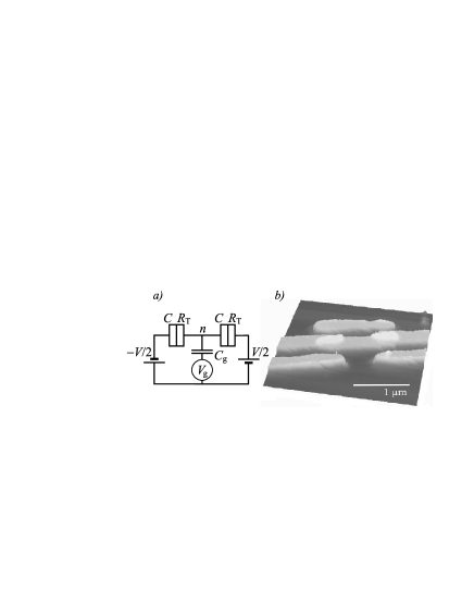
SETs were fabricated with a standard shadow evaporation technique. First 45 nm thick layer of aluminum was evaporated. Aluminum oxide barrier was grown in situ by natural oxidation in pure oxygen atmosphere (20 mbar) in the loading chamber of the UHV system. After oxidation another 45 nm layer of aluminum was deposited from another angle on top of the previously grown oxide layer to form tunnel junctions. Fig. 2 b) shows an AFM image of a typical SET with two Al-AlOx-Al junctions. About 1 nm thick aluminum oxide layer between the aluminum electrodes forms a tunnel junction, which is thin enough to provide quantum mechanical tunneling of electrons through itSET .
II.2 Description of the etching method
The samples were three-dimensionally dry etched by ion beam sputtering in a set-up consisting of a high vacuum (p mbar) experimental chamber equipped with a sample manipulator and TECTRA Electron Cyclotron Resonance (ECR) plasma ion source capable of delivering high current, wide and homogeneous ion beams. Before sputtering, the samples were cleaned with acetone in an ultrasonic bath and subsequently rinsed in isopropanol. Prior to sputtering the surface of the structures was always checked by profiler Tencor P15 that is capable to provide a vertical step height repeatability of 6-7 Å. For dry etching, the samples were bombarded by 1 keV Ar+ ions to a certain fluence using an ion beam current density of about 0.014 mA/cm2. In order to ensure uniform etching over the whole sputtered area, the ions incidence was 60∘ off the surface normal, and the samples were rotated while sputtering. To avoid overheating of the samples exposed to high current ion beam, the sample holder made of copper was cooled with water and the temperature while sputtering was estimated to be close to room temperature. Each sample contained co-evaporated strips, which were partly protected from the ion beam exposure by a droplet of a varnish. After etching the varnish was removed enabling the profilometer control of the surface step between the etched and the non-etched area. Sputtering rates for various materials are listed in the Table 1.
| Aluminum111The aluminum had a natural oxide layer of about 1-2 nm on the surface when sputtered. | SiOx/Si | Bulk Sapphire |
| 1.1 | 3.9 | 0.75 |
Ar+ ions of energy 1 keV impinging on the surface at the angle of 60 degrees with respect to the surface normal practically do not penetrate into the subsurface layers. Penetration depth of the Ar+ ions into Al matrix calculated by SRIM (Stopping and Ranges of Ions Matter) programSRIM for the selected irradiation conditions is less than 15 Å. Taking into account the high rate of the surface sputtering due to high density of the ion current and the glancing incidence, the ion beam etching can be considered as ’a gentle cut’ of the up-most surface atoms without appreciable influence on the underlying layers. The surface of the samples was controlled before and after the ion bombardment with AFM, SEM and profilometer. The influence of the sputtering has a polishing effect, causing no noticeable destruction to the nanostructures.
II.3 Electrical measurements
The superconducting transition of the wires was measured before and after the sputtering sessions. The resistance of the wires as a function of temperature was measured with the four-probe method. The samples were inserted into a directly pumped 4He bath, where the temperature can be tuned with the accuracy of 0.1 mK.
In case of SETs the differential conductance vs. bias voltage characteristics was measured at low voltages ( 10 mV per junction) at liquid helium temperature 4.2 K. The conductance measurements were performed with Nanoway CBT Monitor 400R, an instrument based on an AC resistance bridgenanoway .
III Results and discussion
III.1 Sputtered aluminum nanowires
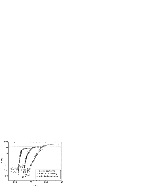
| Original | After 1st sputtering | After 2nd sputtering | |
| [K] | 1.285 | 1.316 | 1.371 |
| [] | 82 | 142 | 380 |
| [mT] | 8.0 | 7.5 | 7.0 |
| [nm] | 15.8 | 12.8 | 9.5 |
| [nm] | 65 | 55 | 39 |
Fig. 3 shows a typical effect of sputtering on the shape of superconducting transition of a wire. It is clearly seen, that the transition becomes wider and the critical temperature tc1 ; tc2 and the normal state resistance changes. All these observations indicate that the wire cross-section has decreased.
The dimensionality of a superconductor is determined by the temperature-dependent coherence length . For the ’dirty limit’ superconductors (mean free path is smaller than ) the effective coherence length Tinkham , where the zero-temperature BCS coherence length for aluminum is m. Thus, formally, any size superconductor sufficiently close to the critical temperature can be considered as ’low-dimensional’. However, if to restrict ourselves to temperatures apart from the fluctuation range and the reasonably ’dirty’ samples ( 10-30 nm), one can consider an aluminum wire with the effective diameter 100 nm ( being the wire cross-section) as one-dimensional (1-D).
The shape of the bottom part of a superconducting transition of not too narrowZaikin ; Golubev 1-D wires is described by the model of temperature activated phase slipsLAMH ; Lukens . The effective resistance exponentially depends on the ratio of the condensation energy of a minimum size superconducting domain of size and the thermal energy LAMH :
| (1) |
where is the normal state resistance, is the length of the wire, is the critical magnetic field, and is the volume of the so-called phase-slip center (minimum size of a superconductor to be driven normal). Coefficient should be of the order of one: , relating the geometrical size to the effective one. The complete expression for the effective resistance used for data fitting includes other termsLAMH , being dependent, for example, on the ratio between the measuring current and the critical current. However, the used measuring currents ( 10 nA) were much smaller than the critical value. Hence, these terms do not contribute quantitatively and are skipped in (1) for simplicity.
The cross-sections obtained from the measurements of the normal state resistance correlate well with the ones used in the fitting procedure (Table 2). The common parameters used for the fits are the sample length m, m, , and the product of resistivity and mean free path m2. The critical temperatures used in fitting procedure (Table 2) correspond well to the experimentally observed onsets of superconductivity (Fig. 3). The increase of the critical temperature with the reduction of the aluminum wire cross-section (and, in general, the thickness of a film) is a well-known effect. Commonly accepted explanation for this phenomenon is not yet settled, while various models are currently discussedtc1 ; tc2 . So far, no traces of the quantum phase slip phenomenaZaikin ; Golubev ; Giordano ; Bezryadin have been detected. At least, down to the aluminum wire effective diameter 30 nm.
The fitting of the experimental data with model calculationsLAMH clearly indicates the reduction of the wire cross-section (Table 2) while subsequent sputtering sessions. The absence of artefacts on the experimental dependencies (Fig. 3) proves that the dry ion etching does not cause ’serious’ damage to the sample (voids or constrictions), but removes the material from the surface gently and in a controllable way. Qualitatively similar results were obtained on few tens of samples.
III.2 Sputtered single electron transistors
A single electron transistor consists of an island isolated from the environment via two tunnel junctions, and a gate electrode which is not important for this study. The characteristic parameter of a single electron transistor is the charging energy, which is the energy required to add one extra electron into the island of an SET,
| (2) |
where is the sum of the capacitances of the junctions and the capacitance of the central island to the ground. Usually it is assumed that the ground capacitance is negligible and the capacitances of the junctions are equal, . The charging energy is of particular interest in this study because it is inversely proportional to the area of the junctions. This can be seen by substituting the expression for the plate capacitor to Eq. (2), where is the junction area, is the thickness and the dielectric constant of an insulating barrier. Thus the charging energy depends on the size of the junctions.
The conductance of a SET as a function of the bias voltage at low temperatures shows a dipCBT . In this study the parameter of interest is the relative height of the dip (Fig. 4), which is proportional to the charging energyCBT :
| (3) |

By measuring the charging energy at liquid helium temperature 4.2 K before and after ion beam etching, one can determine how the areas of junctions have changed by sputtering. Here a natural assumption has been made that the thickness of the insulating layer and its dielectric constant are not altered while etching.
Figure 5 shows the charging energy of different SET samples measured after fabrication and each sputtering session. It is clearly seen that the sputtering increases the charging energy gradually, indicating that the method is capable of reducing the areas of the tunnel junctions. Similar effect has been already observednakamura . As it follows from equation (3), the relative height of the conductance dip is inversely proportional to the junction area. Therefore, one can conclude from the Figure 5, that the junction areas of the sample ”SET5” have reduced by 40 % with respect to the original after three sputtering sessions. The tunnel junction resistances also increased while etching, additionally indicating the reduction of the tunnel junction areas. For instance, in sample ”SET5” the original resistance was 37 k, and it became 84 k after third sputtering. Multisession sputtering was performed on many of the samples without damaging them. Actually the sputtering was not always the cause of the broken SETs; many of those were destroyed while making the electric contacts.
Since the tunnel junctions are formed by thin oxide layers in between aluminum electrodes, there exists a possibility of natural ’aging’ of the samples at normal atmospheric conditions leading to changes of characteristics. Reference measurements were performed to rule out the possibility that charging energy changes ’by itself’ by this natural aging. The charging energy of these samples was measured repeatedly during the time period of several days. No increases in charging energy were observed. So we can be sure that the aging effect is negligible.

In the first sputtering session a surface layer of approximately 25 nm was removed from the electrodes and the island forming the SET. In the following 5-7 nm per session were etched. The behavior of sample ”SET 5” is a bit surprising: although the sputtering conditions and estimated thickness of the removed layers were the same in sessions 2 and 3, the increase of the charging energy is much larger after the third session. It implies that either the sputtering rate changes as the dimensions of the SET structure become smaller, or a certain critical state of the system has been reached.
What could this critical state be? Fig. 6 a) shows a schematic drawing of the SET structure seen from the side just after fabrication.
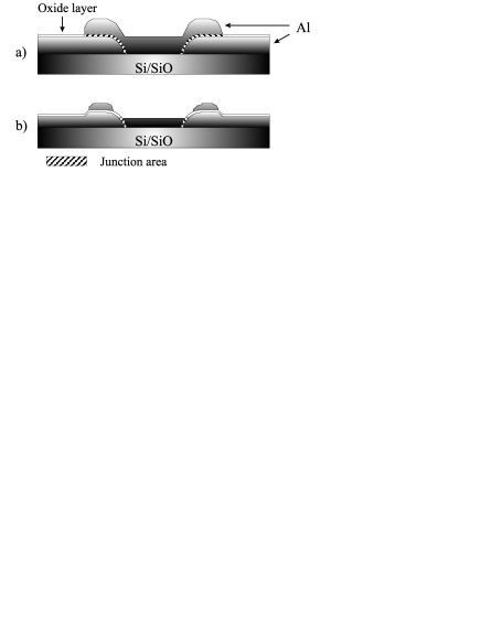
Due to of the shadow evaporation method the metal parts do overlap and the oxide layer gets its characteristic form having approximately vertical and horizontal parts. While sputtering, one finally reaches a state pictured in Fig. 6 b). The metallic contact between the metal of the island and the metal on top of the electrode is lost and ’suddenly’ the effective junction area is much smaller. We assume, that the abrupt increase after third sputtering session for the structure ”SET5” (Fig. 5) is at least partly due to this threshold effect.
The sputtering rate should not be necessarily the same for macroscopically large and nanosized objects. The calibration of sputtering rate in our experiments was done by measuring the height of the step developed between sputtered and non-sputtered regions on the large aluminum contact pads. Although the profilometer provides high vertical resolution (5-7Å), the lateral dimensions of the finest parts in the nanostructures studied were not resolvable. Therefore, if at certain stage of sputtering the etching rate of the finest parts has dramatically increased, this would result in fast reduction of the areas of tunnel junctions and abrupt increase of the observed charging energy, e.g., after third sputtering session (Fig. 5). The possibility of such a scenario is currently under investigation. At present, knowledge about interaction of ions with low dimensional objects, like nanowires, ultra-small tunnel junctions and nano-islands, is rather scarce. Ion sputtering of nanosized objects has not been well explored yet, and various aspects of this method still have to be studied and developed in order to achieve a level suitable for various applications in nanofabrication.
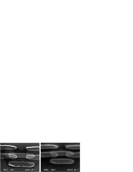
SEM and AFM imaging of the sputtered samples revealed no strongly developed topography on the surface normally attributed to a high fluence ion irradiation. No trenches, craters or other extended defects on the surface were observed. On the contrary, the surface of the sputtered aluminum structures and their topography became smoother after sputtering when compared to as-fabricated state (Fig. 7). It should be noted that single electron transistors are usually considered as very fragile to stay ’alive’ under experimental manipulations. Nevertheless, in our experiments both aluminum nanowires and SETs showed a very high degree of stability under high current ion irradiation. Even those SET samples which were ’destroyed’ in a sense that the resistance became infinite, SEM and AFM observations revealed no breakages or discontinuity. This peculiarity of SETs is still unexplained: they may show infinite resistance and still look perfect. In our experiments any radiation damage fatal for the performance of the wires and SETs should be smaller than 5 nm in size, otherwise they would be detected by our SEM and AFM.
IV Conclusions
We have demonstrated that the ion beam sputtering can be effectively used for reducing the dimensions of prefabricated metallic nanostructures without degradation of their properties and performance. The applicability of the method has been verified with aluminum nanowires and SETs. In the former case, the diameter of the wires was reduced from the initial 60-70 nm down to 30 nm. When the method was applied to SETs, the charging energy was found to increase indicating that the total area of the tunnel junctions decreased. Therefore, it was shown that dimensions of the nanostructures can be reduced by ion sputtering in a controllable and reproducible way.
By virtue of the surface nature of sputtering phenomenon, the method was proved to be very ’gentle’ in a sense that it allows to decrease the dimensions of delicate nanostructures by gradually removing the surface layers without introducing any changes into the interior. Reproducibility and controllability provided by the method imply that ion sputtering is in general applicable to nanoelectronic components and circuits containing nanosized wires and tunnel junctions. The fact that the tunnel junctions ’stay alive’ while sputterings makes the range of applicability of the method wider. For instance the operational temperatures of single electron devices can be extended by increasing the charging energy. It is believed, that bombardment with low energy inert argon gas ions causes no chemical reactions. The method is envisaged to be applicable to circuits based on any kind of metals, semiconductors, insulators and their combinations, regardless of the chemical composition and morphology. Since the method can be applied repeatedly to the same sample, gradual reduction of dimensions is achievable in those applications where the size effect is studied or employed. Instead of fabricating a number of samples of different sizes and comparing their properties and performance, the sputtering method allows to work only with a single sample, thereby, avoiding uncertainties due to the circumstantial factors in fabrication.
Acknowledgements.
This work has been supported by the Academy of Finland under the Finnish Centre of Excellence Programme 2000-2005 (Project No. 44875, Nuclear and Condensed Matter Programme at JYFL) and the EU Commission FP-6 NMP-1 ”ULTRA-1D” project No:505457-1 ”Experinmental and theoretical investication of electron transport in ultra-narrow 1-dimensional nanostructures”.References
- (1) Y. Xia and G.M. Whitesides, Annu. Rev. Mater. Sci., 28, 153 (1998).
- (2) W. Chen and H. Ahmed, Appl. Phys. Lett., 62, 1499 (1993).
- (3) A. Lindell, P. Davidsson and J. Pekola, Microelectronic engineering, 45, 363 (1999).
- (4) A. Lindell, Ph.D. Thesis, Univ. of Jyväskylä, Finland, 2000.
- (5) Yu.A. Pashkin, Y. Nakamura and J.S. Tsai, Appl. Phys. Lett. 76, 2256 (2000).
- (6) J.F. Ziegler, J.P. Biersack and U. Littmark, ”The Stopping and Ranges of Ions in Solids”, (Pergamon, New York, 1985).
- (7) J.P. Pekola, K. P. Hirvi, J. P. Kauppinen and M.A. Paalanen, Phys. Rev. Lett., 73, 2903 (1994); J.P. Kauppinen, K.T. Loberg, A. J. Manninen and J.P. Pekola: ”Coulomb blockade thermometer: Tests and instrumentation”, Review of Scientific Instruments 69 (12), 4166-4175 (1998).
- (8) Detailed description of single charge tunneling phenomena can be found for instance from ”Single Charge Tunneling”, ed. H. Grabert and M.H. Devoret (Plenum Press, New York, 1992).
- (9) Visit Nanoway web site for a detailed measurement principle of CBT Monitor 400R on http://www.nanoway.fi.
- (10) Y. Oreg and A.M. Finkelstein, Phys. Rev. Lett., 83, 191 (1999).
- (11) R.A. Smith, B.S. Handy, and V. Ambegaokar, Phys. Rev. B, 63, 94513-1 (2001).
- (12) M. Tinkham, ”Introduction to superconductivity” (second edition), (McGraw-Hill, Inc., New York, 1996).
- (13) A.D. Zaikin, D.S. Golubev, A. van Otterlo and G.T. Zimányi, Phys. Rev. Lett., 78, 1552 (1997).
- (14) D.S. Golubev and A.D. Zaikin, Phys. Rev. B, 64, 014504 (2001).
- (15) J.S. Langer and V. Ambegaokar, Phys. Rev., 164, 498 (1967); D.E. McCumber and B.I. Halperin, Phys. Rev. B, 1, 1054 (1970).
- (16) J.L. Lukens, R.J. Warburton and W.W. Webb, Phys. Rev. Lett., 25, 1180 (1970); R.S. Newbower, M.R. Beasley and M. Tinkham, Phys. Rev. B, 5, 864 (1972).
- (17) N. Giordano, Physica B 203, 460 (1994).
- (18) A. Bezryadin, C.N. Lau, and M. Tinkham, Nature 404, 971 (2000); C.N. Lau, N. Markovic, M. Bockrath, A. Bezryadin, and M. Tinkham, Phys. Rev. Lett. 87, 217003 (2001).
- (19) Y. Nakamura, D.L. Klein and J.S. Tsai, Appl. Phys. Lett. 68, 275 (1996); and the cited literature.