Circuit with small-capacitance high-quality Nb Josephson junctions
Abstract
We have developed a fabrication process
for nanoscale tunnel junctions
which includes focused-ion-beam etching
from different directions.
By applying the process to a Nb/(Al–)Al2O3/Nb trilayer,
we have fabricated a Nb single-electron transistor (SET),
and characterized the SET at low temperatures, K.
The superconducting gap energy and the transition
temperature of the Nb SET agree with the bulk values,
which suggests high quality Nb junctions.
The single-electron charging energy of the SET is
estimated to be larger than 1 K.
Appl. Phys. Lett. 84, 410 (2004) [DOI: 10.1063/1.1640798]
pacs:
Circuits with Josephson tunnel junctions are one of the most promising candidates for quantum bits (qubits) for quantum computation in solid-state electronic devices.Makhlin et al. (2001); Fitzgerald (2002) The Josephson junctions (JJs) for qubits should have large subgap resistance and an appropriate ratio, where is the Josephson energy and is the charging energy of the junction. The desired range of depends on the degree of freedom (charge, flux, or phase) to be controlled in the circuit. For cases of charge qubitNakamura et al. (1999) and flux qubit,Chiorescu et al. (2003) a typical junction size is on the order of m2, for which the fabrication technique of Josephson tunnel junctions has been well established only for Al/Al2O3/Al junctions. However, materials with larger superconducting gap energy , e.g., Nb (), are more attractive especially for flux qubits, where one wants to have large and keep sufficiently larger than the thermal energy . Note that is proportional to .
There have been a number of attempts to fabricate small-capacitance Al/Al2O3/Nb or Nb/(Al–)Al2O3/Nb JJs.Martinis and Ono (1990); Harada et al. (1994); Pavolotsky et al. (1999); Kim et al. (2002); Dolata et al. (2002, 2003) Conventional nanoscale fabrication processes based on -beam lithography and multiangle shadow evaporation, which work fine for Al/Al2O3/Al JJs, tend to deteriorate the quality of Nb, i.e., and the superconducting temperature are reduced considerably (a summary of this can be found in Fig. 1 of Ref. Dolata et al., 2003). Rather large values of have been obtained in single junctions fabricated by a sloped-edge techniqueMartinis and Ono (1990) ( mV) and in a single-electron transistor (SET) fabricated by a multilayer techniquePavolotsky et al. (1999) (1.35 mV). However, it would be difficult to fabricate multijunction devices using the sloped-edge technique, and the charging energy of the SET fabricated by the multilayer technique was K, which might be acceptable for flux qubits but would be too small for charge qubits and for most single-electron-tunneling devices.
We have developed a process to fabricate high-quality small-capacitance Nb/(Al–)Al2O3/Nb JJs which includes focused-ion-beam (FIB) etching from two different directions. By employing the process, we have fabricated SETs with a three-dimensional structure, shown in Fig. 1.
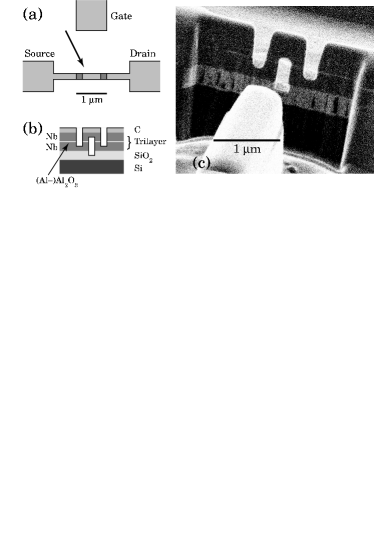
Details of the process are as follows. A trilayer of Nb (thickness: 0.3 m), Al (0.01 m)–Al2O3 (1 nm), and Nb (0.3 m) was sputtered onto a SiO2/Si substrate in a single vacuum cycle. The Al2O3 layer was formed by oxidizing the surface of Al. The film was then patterned with standard photolithography and Ar+ milling, where the smallest feature size in this step was 5 m. The dimensions of the trilayer were decreased further in a Ga+ FIB system, which has three functions: deposition, etching, and observation. From the direction perpendicular to the substrate, we first deposited C (thickness: 0.1 m) by decomposing phenanthrene (C14H10) gas with a Ga+ beam current of 48 pA. The role of the C layer is to minimize damage of the trilayer by Ga+ during the etching process described below. Then, we etched into the pattern shown in Fig. 1(a) except for the fine structure on the narrow track between the source and the drain. For etching, we used two beam currents, 1.3 nA (rough etching) and 9 pA, not only for efficiency but also to minimize the amount of material redeposited on the sides of the narrow track. After tilting the substrate 88∘, three holes were made with a 9 pA beam current on the side of the track as shown in Fig. 1(b). A double-junction structure formed between the holes. An example of the SET fabricated in the above process is shown in Fig. 1(c), which is a secondary-electron image taken in the same FIB system. The final step in our fabrication process is anodization, and there are two reasons for this. One is to eliminate completely short circuit of the junction due to conducting materials (mostly Nb) redeposited during FIB etching, by changing the conducting materials into insulating oxides. The other is to suppress the contribution of the sample surface, which might have been damaged by Ga+, to electrical conduction. Because anodization also reduces the effective area of the junctions, we designed the initial junction size delineated by the FIB to be m2, although we could fabricate much smaller junctions by this technique. We kept the anodization current constant at a value in the range 1–10 A/cm2 and, for the sample discussed below, we anodized up to 60 V, which reduced the effective junction area to m2. The FIB etching was quite reproducible, although the resistance of the SET after anodization varied from sample to sample.
We measured the samples in a 4He continuous-flow cryostat with a Si-diode thermometer mounted next to the sample holder. The current-voltage (-) characteristics of one of the samples at K is shown in Fig. 2.

The - curve exhibits a sharp superconducting gap, whose value corresponds to two Nb JJs. We obtained mV from the distance between the peaks in the differential conductance vs curve (see the lower data set of Fig. 2). Here the charging energy of the SET is negligibly small for the estimate of as will be discussed later. This value of 1.4 mV is the largest for m2 junctions. Moreover, it agrees with the values at liquid 4He temperatures for 1–10 m scale JJs fabricated by a standard photolithographic technology for integrated JJ circuits. We also measured the temperature dependence of the - curve in order to determine . The - curve looks almost linear at K. However, when we look at the differential resistance , it is easy to find a qualitative difference between the vs curves at K and those at K. The inset of Fig. 3 shows the vs curve at and 9.2 K.
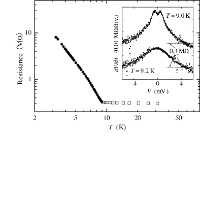
The curve at 9.0 K has a dip in the middle, while that at 9.2 K does not. Based on this qualitative difference, we determine that K, which agrees with the bulk value of 9.2 K within the error. Here 0.2 K includes all errors in thermometry and determination. We confirm the adequacy of the above determination in Fig. 3 by plotting versus the zero-bias resistance for K (normal state) and the subgap resistance for K (superconducting state), where we have defined the subgap resistance as the maximum value of . From the values of and , we conclude that the quality of our JJs is high and it has not deteriorated in the FIB etching process.
Let us look at the properties of the sample as an SET. The gate electrode is located 1 m from the double-junction system (Fig. 1), and the voltage applied to the gate modulates the current even up to 5 K (data not shown). Thus, the sample indeed works as an SET. In order to characterize the sample further, we cooled it down to 0.04 K in a 3He–4He dilution refrigerator. At K, the subgap resistance becomes 102 M, which is significantly larger than the normal-state resistance, 0.3 M, and again, suggests high quality junctions.
The parameters of a SET, such as the capacitances and of the tunnel junctions and the capacitance between the island electrode and the gate electrode, can be determined by measuring the blockade of single-electron tunneling in the normal state at a low enough temperature.Ingold and Nazarov (1992) We drove the Nb SET into the normal state by applying a magnetic field of 2.7 T perpendicular to the substrate, and measured - curves for different values of at K. An example of the - curve, which is for mV, is shown in the lower data set of Fig. 4.

One period in the axis corresponds to , so that aF, which is consistent with the geometry. In the upper data set of Fig. 4, we estimate the zero-current region at on the - plane (Coulomb diamond). The horizontal dotted line corresponds to of the SET. Thus, from mV in Fig. 4, we obtain K, which is consistent with the effective junction area of m2 and sufficiently larger than the base temperature of a typical dilution refrigerator, 0.1 K. When which is the case in our Nb SET, and are estimated from the slopes of the solid lines in Fig. 4. We find that , although we designed it so that .
The reason for asymmetry in the junction capacitance is that we had to anodize the SET up to a large voltage in order to eliminate the short circuit. The accuracy of the capacitances could be improved by introducing a step of reactive-gas-assisted etching at the end of the FIB process. We have already confirmed that XeF2 gas enhances the etching rate of Nb 102 times and “cleans up” redeposited Nb. By introducing the step, we would be able to reduce the anodization voltage considerably. Reducing the anodizaiton voltage would also improve the yield of the fabrication process.
It should be noted that our process is also applicable to more complex circuits. Moreover, it is much more flexible in terms of circuit pattern than the conventional technique based on -beam lithography and shadow evaporation, or the multilayer technique in Ref. Pavolotsky et al., 1999. Very recently, a similar FIB-etching technique was independently developed, and nanoscale single junctions with a variety of materials were fabricated. Bell et al. (2003) Thus, the process is not limited to Nb/(Al–)Al2O3/Nb junctions.
In the superconducting state, one expects that the supercurrent flowing through the SET depends on periodicallyJoyez (1995) and that the period is ( periodic). In many experiments, however, a period of ( periodic), which suggests the existence of subgap quasiparticle states,Joyez (1995) has also been seen. In small-capacitance Al/Al2O3/Nb or Nb/(Al–)Al2O3/Nb systems, only periodicity has been reported. In our Nb SET, the measured supercurrent at K and is also periodic, and its magnitude is on the order of 10 pA, which is 10-3 the theoretical maximum, , where is the Ambegaokar-Baratoff critical current and is the normal-state resistance of the junction. Further investigation of the periodicity by measuring high-quality Nb SETs with different parameters would clarify whether the periodicity is intrinsic to Nb or not.
In summary, we have fabricated a high-quality Nb SET with K by developing a fabrication process for nanoscale tunnel junctions. The process is much more flexible than conventional ones based on -beam lithography.
The authors are grateful to Y. Kitagawa for preparation of the Nb/(Al–)Al2O3/Nb trilayer, to M. Ishida for assistance with the FIB system, to H. Akaike for valuable comments on anodization, and to Yu. Pashkin, T. Yamamoto, and O. Astafiev for fruitful discussions. This work was supported in part by the Special Postdoctoral Researchers Program of RIKEN and by MEXT.KAKENHI (Grant No. 15740190).
References
- Makhlin et al. (2001) Yu. Makhlin, G. Schön, and A. Shnirman, Rev. Mod. Phys. 73, 357 (2001).
- Fitzgerald (2002) R. Fitzgerald, Phys. Today 55, (6), 14 (2002).
- Nakamura et al. (1999) Y. Nakamura, Yu. A. Pashkin, and J. S. Tsai, Nature (London) 398, 786 (1999).
- Chiorescu et al. (2003) I. Chiorescu, Y. Nakamura, C. J. P. M. Harmans, and J. E. Mooij, Science 299, 1869 (2003).
- Martinis and Ono (1990) J. M. Martinis and R. H. Ono, Appl. Phys. Lett. 57, 629 (1990).
- Harada et al. (1994) Y. Harada, D. B. Haviland, P. Delsing, C. D. Chen, and T. Claeson, Appl. Phys. Lett. 65, 636 (1994).
- Pavolotsky et al. (1999) A. B. Pavolotsky, T. Weimann, H. Scherer, V. A. Krupenin, J. Niemeyer, and A. B. Zorin, J. Vac. Sci. Technol. B 17, 230 (1999).
- Kim et al. (2002) N. Kim, K. Hansen, J. Toppari, T. Suppula, and J. Pekola, J. Vac. Sci. Technol. B 20, 386 (2002).
- Dolata et al. (2002) R. Dolata, H. Scherer, A. B. Zorin, and J. Niemeyer, Appl. Phys. Lett. 80, 2776 (2002).
- Dolata et al. (2003) R. Dolata, H. Scherer, A. B. Zorin, and J. Niemeyer, J. Vac. Sci. Technol. B 21, 775 (2003).
- Ingold and Nazarov (1992) G.-L. Ingold and Yu. V. Nazarov, in Single Charge Tunneling, edited by H. Grabert and M. H. Devoret (Plenum, New York, 1992), chap. 2.
- Bell et al. (2003) C. Bell, G. Burnell, D.-J. Kang, R. H. Hadfield, M. J. Kappers, and M. G. Blamire, Nanotechnology 14, 630 (2003).
- Joyez (1995) P. Joyez, Ph.D. thesis, Univ. of Paris 6, Paris France (1995).