Role of microstructure in porous silicon gas sensors for NO2
Abstract
Electrical conductivity of porous silicon fabricated form heavily doped p-type silicon is very sensitive to NO2, even at concentrations below 100 ppb. However, sensitivity strongly depends on the porous microstructure. The structural difference between sensitive and insensitive samples is independently confirmed by microscopy images and by light scattering behavior. A way to change the structure is by modifying the composition of the electrochemical solution. We have found that best results are achieved using ethanoic solutions with HF concentration levels between 13% and 15%.
Porous silicon (PSi) is an interesting material for gas sensing Sailor (1997). Physical properties of PSi, such as DC electrical conductivity, are very sensitive to the environment Bilenko et al. (1997). Detection of NO2 at concentration levels as low as 12 ppb has been demonstrated Pancheri et al. (2003). Thus, PSi is an intriguing material for NO2 sensors. NO2 is a well known air pollutant, originated by internal combustion engines, whose attention level is set at around 100 ppb by pollution normatives.
Exposure of PSi to NO2 leads to an increase of DC conductivity. The effect has been observed on PSi fabricated from heavily doped p-type (p+) substrates (resistivity in the m Ω c m range). High sensitivity is reported in thick samples (at least some tens of µ m ), and in the porosity range between 50% and 80% Boarino et al. (2000); Baratto et al. (2001); Timoshenko et al. (2001); Boarino et al. (2001); Pancheri et al. (2003).
Porous layers obtained from heavily p-type doped wafers have low conductivity, even though the boron dopants are not significantly removed during the anodization process; boron concentration is comparable in PSi and bulk Si Polisski et al. (1998, 1999). It is argued that one of the relevant effects of anodization to the conductivity is to leave the dopant ions at close distance from the surface, where defects trap free carriers, thus inhibiting dopants’ acceptor function and lowering the porous layer conductivity Polisski et al. (1998, 1999); Timoshenko et al. (2001); Boarino et al. (2001). Mobility is also lower in PSi Timoshenko et al. (2001). Under exposure to NO2, the hole concentration increases, thus suggesting that the acceptor function of boron dopants is re-activated by NO2 Timoshenko et al. (2001); Boarino et al. (2001). A characterization of the effect at different porosity levels has been performed Boarino et al. (2000). However, porosity is not an exhaustive parameter to link the sensitivity and the microstructure of PSi. To our knowledge, it has not been hitherto shown whether the microstructure of PSi plays a role in the sensitivity to NO2. The aim of this work is to demonstrate that the microstructure has a critical role in such sensitivity.
PSi layers were grown by electrochemical dissolution in an HF-based solution on a single-crystalline p-type (100) heavily-doped Si substrate. Substrate nominal resistivity was 6-15 m Ω c m . Before the anodization, the native oxide was removed from the backside of the wafers, and aluminium back contacts were deposited by evaporation. The anodizing solution was obtained by mixing aqueous HF (48% wt.) with ethanol. We have tested different solutions, introducing small variations in the final nominal concentration of HF, which was ranging between 13% and 15% wt. As expected, lower (higher) HF concentration led to higher (lower) porosity samples Bisi et al. (2000). The etching was performed by applying an etching current density of 50 m A / c m ^ 2 for 23 minutes. After anodization, the samples where rinsed in ethanol and pentane, and dried in ambient air. Gold electrodes were deposited by evaporation on the PSi top surface. Special care was taken to achieve the same electrode size on all the samples. Copper wires were connected to the gold electrodes using an epoxy silver paste. Thickness and refractive index of samples were extracted from normal reflectance spectra and Scanning Electron Microscopy (SEM) images. Using Bruggeman approximation we have estimated the porosity from the measured refractive index Bisi et al. (2000). Microstructure was characterized with Transmission Electron Microscopy (TEM) measurements.
During measurements in presence of NO2 and water vapor, the sensors were biased between one of the top contacts and the back contact at a constant voltage, while the current was measured. The sensors were kept in a sealed chamber under controlled flux of gases coming from certified cylinders. Humid air was obtained by flowing dry air through a bubbler. Different relative humidity levels and NO2 concentrations were obtained mixing humid air, dry air and a dilute solution of NO2 in air (550 ppb) with a flow control system. Relative humidity was monitored using a calibrated hygrometer.
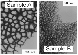
Figure 1 shows the TEM images of two samples. The porosity of Sample A and B was, respectively, 78% and 60%. In Figure 2, we show the effect of exposure to water vapor (at 30% and 70% levels of relative humidity) and to NO2 at 50 ppb concentration.
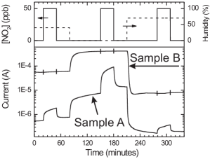
In Figure 2, no resistivity change is observed in the 60% porosity sensor (Sample B) under exposure to NO2 (50 ppb), as opposed to the 78% porosity sensor (Sample A). One might be initially tempted to conclude that higher porosity leads to higher sensitivity to NO2. However, a different conclusion would be drawn from other reports, in which samples with 60% porosity showed higher sensitivity than samples with 75% porosity (the thickness and substrate resistivity were comparable to this work) Boarino et al. (2000).
The peculiarity of our fabrication procedure is low HF concentration. At the HF concentration and the current density of this work (respectively, 13%-15% and 50 m A / c m ^ 2 ), the anodization is close to the electropolishing regime Bisi et al. (2000). In these conditions, and especially at the lower HF concentration, anodization is quite aggressive. In p+ samples, the etching should evolve selectively around the dopants, leaving them in place Polisski et al. (1999). However, during anodization of Sample A, several boron dopants have been removed. In fact, the boron density of these samples (N/ c m ^ 3 ) implies the presence of about 1 ion every 2 or 3 n m along any linear direction, whereas Sample A has empty gaps of several tens of n m (Figure 1).
Changes in the solutions in aggressive conditions lead to differences in conductivity which go beyond the difference of porosity. For example, from the porosity difference, the amount of leftover Si in Sample A (78% porosity) is about two times less than in Sample B (60% porosity). One might expect the resistance of the two samples to differ by a comparable factor. However, the resistance is 2 orders of magnitude larger in Sample A (Figure 2). A possible relevance of quantum confinement effects can be probably excluded, considering that the cross sections of the resistive paths appear to have diameter larger than a few n m (Figure 1). Figure 1 might even suggest that Sample B has conductive channels with smaller cross sections. In this latter case, any relevance of the size of the cross section would make the 2 orders of magnitude difference in conductivity even more surprising, because it could only increase the effective resistivity of Sample B.
Beside porosity, a structural difference is apparent by comparing the TEM images. The Si structures of Sample B are more branching and interconnecting with each other than those of Sample A. This is confirmed both by side-views TEM images of pore walls (not shown), and by light scattering experiments (Figure 3, experimental data shown elsewhere Otón et al. (2002); Oton et al. (2003)).
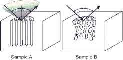
The light scattering behavior cannot be discussed on the only basis of porosity difference. On the contrary, the scattering of Sample A can be quantitatively explained as a structural feature. It is originated by the straight pore walls, as discussed in greater detail elsewhere Otón et al. (2002); Oton et al. (2003). The markedly different light scattering behavior strongly emphasizes the microstructural difference between the two samples.
Aggressive anodization leads to high sensitivity to NO2 (Figure 2). We propose the following connection between microstructure and sensitivity.
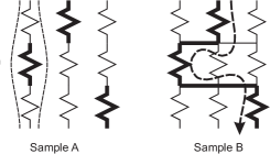
The resistors of Figure 4 represent local resistance along pore walls. Pore walls of Sample A are less interconnected, thus high resistance portions are less likely to have local bypasses with lower resistance. Therefore, high resistivity paths dominate in the total Sample A resistance. The highly resistive pore walls are the most sensitive to NO2, since thinner walls have larger fraction of dopants at close distance from the surface. NO2 locally reactivates the acceptor dopant, thus reverting the high resistivity to lower resistivity paths. In the case of Sample B, the presence of bypasses, whose resistance is low even in absence of NO2, obscures the effect of NO2. This interpretation qualitatively agrees with both the large difference of resistance and the difference of sensitivity to NO2.
The fact that both sensors are similarly sensitive to water probably depends on the much larger amount of water molecules, which acts as donors Kiselev and Krylov (1987) and tend to increase the resistance in all the porous layer.
In conclusion, DC electrical conductivity of heavily doped porous silicon can be very sensitive to NO2. The comparison of our results with past literature shows that there is no univocal relationship between sensitivity and porosity. In this work, we have compared light scattering, TEM images, and sensing performance of porous silicon samples. Our results suggest that the structure of porous silicon is determinant towards high sensitivity to NO2. The microstructure depends on the composition of the electrochemical solution used for the anodization. A way to achieve very sensitive structures to NO2 is by using electrochemical solutions with low HF concentrations (13%). The detectable level of NO2 in air is well below 100 ppb, the threshold for realistic applications.
We acknowledge the help of Prof. S. Gialanella (Facoltà di Ingegneria, Università di Trento) for the TEM measurements, the support of INFM, progetto PAIS 2001 ”SMOG”, of Provincia Autonoma di Trento and of Science and Technology Ministry of Spain (MCYT) (Project No. MAT 2002-00044). C. O. acknowledges University of La Laguna and Cajacanarias for the fellowship ”Beca de investigación para doctorandos” (2003).
References
- Sailor (1997) M. J. Sailor, in Properties of Porous Silicon, edited by L. Canham (London, U.K., 1997), IEE Inspec, p. 364.
- Bilenko et al. (1997) D. Bilenko, O. Belobrovaya, E. Jarkova, O. Coldobanova, I. Mysenko, and E. Kashina, Sensors and Actuators A 62, 621 (1997).
- Pancheri et al. (2003) L. Pancheri, C. J. Otón, Z. Gaburro, G. Soncini, and L. Pavesi, Sensors and Actuators B 89, 237 (2003).
- Boarino et al. (2000) L. Boarino, C. Baratto, F. Geobaldo, G. Amato, E. Comini, A. M. Rossi, G. Faglia, G. Lérondel, and G. Sberveglieri, Materials Science and Engineering B 69-70, 210 (2000).
- Baratto et al. (2001) C. Baratto, G. Faglia, G. Sberveglieri, L. Boarino, A. M. Rossi, and G. Amato, Thin Solid Films 391, 261 (2001).
- Timoshenko et al. (2001) V. Y. Timoshenko, T. Dittrich, V. Lysenko, M. G. Lisachenko, and F. Koch, Physical Review B 64, 085314 (2001).
- Boarino et al. (2001) L. Boarino, F. Geobaldo, S. Borini, A. M. Rossi, P. Rivolo, M. Rocchia, E. Garrone, and G. Amato, Physical Review B 64, 205308 (2001).
- Polisski et al. (1998) G. Polisski, G. Dollinger, A. Bergmaier, D. Kovalev, H. Heckler, and F. Koch, phys. stat. sol. (a) 168, R1 (1998).
- Polisski et al. (1999) G. Polisski, D. Kovalev, G. Dollinger, T. Sulima, and F. Koch, Physica B 263-274, 951 (1999).
- Bisi et al. (2000) O. Bisi, S. Ossicini, and L. Pavesi, Surface Science Reports 38, 1 (2000).
- Otón et al. (2002) C. J. Otón, Z. Gaburro, M. Ghulinyan, L. Pancheri, P. Bettotti, L. Dal Negro, and L. Pavesi, Appl. Phys. Lett. 81, 4919 (2002).
- Oton et al. (2003) C. J. Oton, M. Ghulinyan, Z. Gaburro, P. Bettotti, L. Pavesi, L. Pancheri, S. Gialanella, and N. E. Capuj, Journal of Applied Physics 94, in print (2003).
- Kiselev and Krylov (1987) V. F. Kiselev and O. V. Krylov, Electronic Phenomena in Adsorption and Cathalisis on Semiconductors and Dielectrics (Springer, Berlin, 1987).