A MAGNETIC-FIELD-EFFECT TRANSISTOR AND SPIN TRANSPORT
Abstract
A magnetic-field-effect transistor is proposed that generates a spin-polarized current and exhibits a giant negative magnetoresitance. The device consists of a nonmagnetic conducting channel (wire or strip) wrapped, or sandwiched, by a grounded magnetic shell. The process underlying the operation of the device is the withdrawal of one of the spin components from the channel, and its dissipation through the grounded boundaries of the magnetic shell, resulting in a spin-polarized current in the nonmagnetic channel. The device may generate an almost fully spin-polarized current, and a giant negative magnetoresistance effect is predicted.
pacs:
72.25.Hg, 72.25Mk, 73.40.Sx, 73.61.GaSpintronic devices for storage and transport of information and for quantum computations have been the subject of increasing interest Aws ; Dat .
Here we propose a scheme for a magnetic-field-effect transistor (MFET), where the electric current flow is governed by a magnetic field in contrast to conventional electronic devices (e.g. the silicon-based FET) which are controlled by an electric field. The purpose of the proposed spin-guide scheme pertains to generation and transport of electric currents characterized by a high degree of spin-polarization.
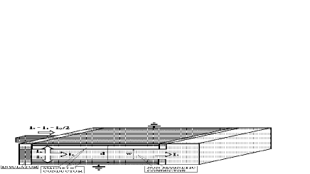
We propose to use a “sandwich” configuration, with a nonmagnetic (NM) conducting channel and a surrounding magnetic material (MM) whose external boundaries are grounded (see Fig. 1). Electric current flows parallel to the NM/MM interface, instead of being normal to it as in a spin-filter Aro ; Son ; Mol2 . Underlying the operation of the device is the removal of one of the current spin-components from the NM channel, whereas in the spin-filter scheme spin polarization in a NM conductor is created by electrons injected from a magnetic material.
Let an unpolarized constant current be driven through the channel entrance. Away from the channel entrance a difference will develop between the spin-up and spin-down currents. Non-equilibrium electrons with one of the spin directions (that coincides with the majority-spin direction in the magnetic layer, spin-down for example) will preferentially leave the nonmagnetic channel - that is, the transparency of the NM/MM interface is different for spin-up and spin-down electrons due to the conductivity difference in these materials. With high probability (particularly for a thin magnetic shell) these electrons will dissipate at the grounded external boundary without return to the channel. Consequently, a polarized electric current is generated in the channel with the polarization increasing as a function of the distance from the channel entrance (due to depletion of the spin-down carriers).
For implementation of the device we consider two classes of magnetic materials for the magnetic shell. (1) Dilute II-VI magnetic semiconductors (DMS): these compounds may have a sufficiently high degree of spin polarization Mol2 because of the very large Zeeman splitting of the spin subbands. When the Fermi level in the DMS lies below the bottom of one of the spin subbands, nearly full spin-polarization of the DMS may be reached. Thus, using a DMS (consisting e.g. of (Zn,Mn,Be)Se as the MM) and a lattice matched (Zn,Be)Se as the NM channel, one may achieve conditions where all the electrons in the magnetic material are fully spin-polarized and the magnetic shell will not transmit electrons with one of the spin directions (spin-up in our example, see Fig. 1). (2) Alternatively, ferromagnetic metals (like Ni, Fe or Co) may be used for the magnetic shell. In contrast to ordinary electronic devices where a combination of a metal with a semiconductor is used, our scheme may be implemented as an all-metal device
The above device exhibits sensitivity to changes in the magnetic field. Indeed, the aforementioned selective transparency of the NM/MM interface provides different decay length-scales for the spin-up and spin-down electrons along the channel. Therefore, if we create an unmagnetized magnetic shell by switching-off the magnetic field, the dissipation of all the non-equilibrium electrons (i.e. of both spin directions) at the grounded boundary will be faster then the rate of their arrival to the channel exit, i.e. almost all the electrons may not reach the exit of the spin guide because of a larger probability to dissipate to the grounding. Thus, by changing the applied magnetic field we may change significantly the resistance of the spin-guide device (that is, a strong negative magnetoresistance effect is predicted), and it may operate as a transistor governed by the magnetic field, i.e. a MFET.
Consider - the non-equilibrium parts of the electrochemical potentials for the two spin directions. In the diffusive regime, the spin transport is described by (see, e.g. Son )
| (1) |
where , are the densities of states at the Fermi level of the up and down spins, is the spin-flip scattering time, and are the corresponding conductivities. Eqs.(1) holds under the assumption that both the spin-flip mean-free-paths ( are the Fermi velocities of the spin-up and spin-down electrons), and the widths of the channel () and the magnetic shell () exceed significantly the diffusion step-lengths i.e. ; otherwise, the problem should be treated within the kinetic equation approach. The electric current densities are related to the electrochemical potentials via Ohm’s law.
Let the axis lie in the middle of the channel and be directed along it, and take the axis to be perpendicular to the interfacial planes, with the origin of the coordinate system located in the center of the entrance into the channel (see Fig.1). The conductivity of the NM channel is spin independent and constant (), and we impose the boundary conditions at reflecting the grounding of the external planar boundaries. The solutions of Eq.(1) that we seek consist of a sum of terms, with each expressed as products of two functions, one depending on the x-variable and the other depending on the z-coordinate and on the discrete indices “” (see Eq. (6) below). To find the general solution of Eq.(1) we introduce the functions , where the functions are the -dependent parts (multiplying exponential decay factors in the -direction ) of the special solutions of Eq.(1), . Due to the symmetry of the system we obtain
| (4) | |||
where the diffusion length is the characteristic length-scale for equilibration of the spin subsystems in the magnetic (M) and nonmagnetic (N) regions, respectively, (with the corresponding subscripts M and N as appropriate), . The functions have to satisfy the equations
| (5) |
Rewriting Eq.(5) for the functions we obtain an equation for the eigenfunctions of a self-adjoint operator with the eigenvalues . A full set of the solutions of Eq.(5) corresponding to the possible values of the parameters is a complete basis set in the interval . Consequently, the general solution of Eq.(1) is given by
| (6) | |||
where the constants are determined by the boundary conditions at the ends of the spin-guide, in conjunction with the orthogonality of the functions for different values. The current densities at the channel entrance () are given by , and for at , where is the spin-guide length, we obtain
| (7) |
The coefficients (see Eq.(4)) are determined by matching the functions and the currents (i.e. the derivatives ) at (see Fu ). The possible values of the damping parameter may be found from the consistency condition of these equations
| (8) | ||||
If constant current is injected into the NM channel only (i.e. at : at and at ), and restricting ourselves to current variation only in the direction (i.e. averaging in the transverse, , direction), the current in the channel is given by
| (9) |
From the above we can calculate the degree of spin-polarization of the current in the channel, . The solutions given in Eq.(9) exhibit exponential decreases along the channel, with different decay rates for the two spin directions. The main contribution to the spin-up current is where is the smallest solution from the set determined by Eq.(A MAGNETIC-FIELD-EFFECT TRANSISTOR AND SPIN TRANSPORT), while the spin-down current decays much faster , where . Thus, inside the spin-guide the spin polarization of the current in the nonmagnetic channel will tend exponentially to unity, i.e. ; for further details see Fu .
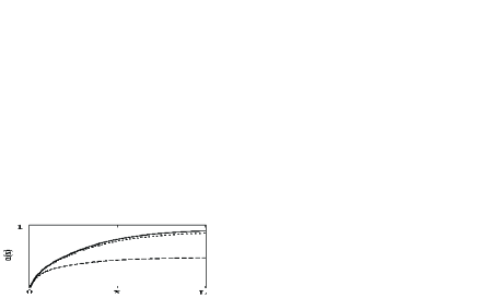
In Fig.2 we display the -dependence of the degree of spin-polarization calculated from Eq.(9). These curves demonstrate exponential growth of the degree of spin-polarization with distance from the entrance. In general, the saturation value is dependent on spin-flip processes in the materials used for the device. Comparison of the curves for different illustrates that higher current polarization is achieved for smaller ratios between the width of the NM channel and the spin-flip length . The current and spin polarization in the device may be manipulated and tuned continuously with an applied magnetic field. Indeed, by changing the magnetic field the ratio / can be changed, and one may tune the current decay parameter k (see Eq.(A MAGNETIC-FIELD-EFFECT TRANSISTOR AND SPIN TRANSPORT)).
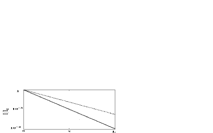
Switching-off of the magnetic field increases the damping factor of the current from the value (in the case of an ideal magnetic material shell Fu ) up to which depends on the ratio of the conductivities of the unmagnetized (UM) shell and the NM channel: ; for the present case this equation replaces Eq.(A MAGNETIC-FIELD-EFFECT TRANSISTOR AND SPIN TRANSPORT). When we obtain . Fig.3 depicts the variation of the current along the nonmagnetic channel when a magnetized (dotted line) or an unmagnetized (solid line) shell is used - the current changes by about three orders of magnitude at the exit () of the MFET. When the difference between and is small and the field effect is also small. Increase of the NN/MM interface resistance (e.g. via adding barriers), will enhance the effect.
A giant negative magnetoresistance effect may be observed by switching the magnetization directions in the upper and lower magnetic layers from being parallel to each other, to having antiparallel directions. When the upper and lower magnetic layers have parallel magnetization directions, a polarized current will arrive at the channel exit, since electrons with only one spin direction will be transported preferentially through the magnetic layers to the grounding. In contrast, when the magnetic layers’ magnetizations are antiparallel, the output current will be unpolarized and it will decrease significantly in magnitude. This effect could be of particular interest in the case of a ferromagnetic metal shell where residual magnetization may remain (because of domain structure) upon switching-off the magnetic field.
In summary, we proposed a scheme for a magnetic-field-effect transistor, i.e. a device for generation of highly spin-polarized currents, whose operation is governed by a magnetic field. In this device nearly complete current spin-polarization may be achieved, even when a magnetic shell with a lower degree of spin polarization is used. Large changes in the current may be brought about through on/off switching of a magnetic field. Furthermore, the magnetic-field sensitivity suggests the MFET as a magnetic-field-sensor. Finally, the wide range of measured spin-diffusion lengths (typically of the order of nm in metals and microns in semiconductors To ) suggests the potential fabrication of nano-scale MFET devices, with possible incorporation of known nanostructures (e.g. nanotubes as the conducting channel).
This research was supported by Grant No. UP2-2430-KH-02 of the CRDF and by the US DOE Grant No. FG05-86ER-45234 (E.N.B and U.L.).
-
(1)
Semiconductor Spintronics and Quantum
Computation, eds. D. D. Awschalom, D. Loss, and N. Samarth,
Springer, Berlin, 2002.
- (2) S. Datta and B. Das, Appl. Phys. Lett. 56, 665 (1990).
- (3) A.G. Aronov, JETP Lett. 24, 32 (1976).
- (4) P. C. van Son, H. van Kempen, and P. Wyder Phys. Rev. Lett. 58, 2271 (1987).
- (5) G. Schmidt, G. Richter, P. Grabs, C. Gould, D. Ferrand, and L. W. Molenkamp, Phys. Rev. Lett. 87, 227203 (2001).
- (6) R.N.Gurzhi, A.N.Kalinenko, A.I.Kopeliovich, A.V.Yanovsky, E.N.Bogachek, and Uzi Landman, Phys. Rev. B 68, 125113 (2003).
- (7) Spin electronics, eds. M. Ziese, M.J.Thornton, Springer, Berlin; New York, 2001.
- (2) S. Datta and B. Das, Appl. Phys. Lett. 56, 665 (1990).