Energy levels in polarization superlattices: a comparison of continuum strain models
Abstract
A theoretical model for the energy levels in polarization superlattices is presented. The model includes the effect of strain on the local polarization-induced electric fields and the subsequent effect on the energy levels. Two continuum strain models are contrasted. One is the standard strain model derived from Hooke’s law that is typically used to calculate energy levels in polarization superlattices and quantum wells. The other is a fully-coupled strain model derived from the thermodynamic equation of state for piezoelectric materials. The latter is more complete and applicable to strongly piezoelectric materials where corrections to the standard model are significant. The underlying theory has been applied to AlGaN/GaN superlattices and quantum wells. It is found that the fully-coupled strain model yields very different electric fields from the standard model. The calculated intersubband transition energies are shifted by approximately 5 – 19 meV, depending on the structure. Thus from a device standpoint, the effect of applying the fully-coupled model produces a very measurable shift in the peak wavelength. This result has implications for the design of AlGaN/GaN optical switches.
pacs:
73.21.Ac, 71.20.Nr, 85.30.Tv, 73.20.At, 73.61.Ey, 77.65.LyI Introduction
Intersubband optical transitions (ISBT) in AlGaN/GaN superlattices (SLs) and multiple quantum wells (MQWs) are being exploited for use in near- and mid-infrared lasers and ultra-fast all-optical switches in the 1.5 – 3 m wavelength range.Suzuki and Iizuka (1997, 1998, 1999); Iizuka et al. (2000); Heber et al. (2002); Iizuka et al. (2002); Kishino et al. (2002) A key design issue related to ISBT-based device concepts is the calculation of the electron energy levels of these structures so that the peak wavelengths can be estimated before growth and fabrication. In the present work, we investigate the role of strain and polarization on the subband structure of SLs in the wurtzite crystal structure. Through a theoretical examination of fully-coupled and semi-coupled electromechanical treatments we show the importance of using a fully-coupled model for predicting the energy levels of SLs in strongly piezoelectric material systems. The model is then used to predict the energy levels of ten actual structures in order to compare our calculated ISBTs to previously measured spectra.
Unlike zincblende semiconductor SLs, a number of issues arise in wurtzite SLs that complicate the task of calculating the energy levels. AlGaN in the wurtzite phase has a large spontaneous polarization moment along the axis. In addition, SLs grown on a SiC or sapphire substrate are pseudomorphic and the large in-plane biaxial strains induce a piezoelectric polarization moment oriented along the -axis with the direction depending on whether the strain is tensile (SiC) or compressive (Al203). The discontinuity of the polarization moments effectively represents fixed sheet charges at the interfaces of the SL. In general, each AlGaN on GaN interface in the direction will have a positive space charge and each GaN on AlGaN interface a negative space charge. Thus unlike zincblende SLs which are flat band unless doped, a calculation of the electronic eigenvalues using the Schrödinger equation must be preceded by a calculation of the electrostatic potential, representing the Hartree term in the Schrödinger equation, using the Poisson equation.
There is a further complication that has been previously ignored in calculations of the energies in AlGaN/GaN SLs. This involves the incorporation of strain into the electric field and eigenvalue calculations. To date, the strain model for AlGaN/GaN SLs has been borrowed from the zincblende realmSmith and Mailhiot (1990) without additional consideration given to its validity for strongly piezoelectric materials. Although piezoelectric, zincblende materials have comparatively small piezoelectric tensor elements so that the thermodynamic equation of state is reduced to the standard Hooke’s law with little or no error. From this relation, the strain tensor for zincblende SLs can be readily worked out with good accuracy. On the other hand, wurtzite materials have large piezoelectric coefficients indicating strong coupling between the strain and electric fields. In the present case of group III-nitride materials, we will show that treating the mechanical strain as separate from the electronic properties is no longer a sound methodology. The result is that a linear stress-strain model (Hooke’s law) is no longer valid, and the fully-coupled thermodynamic equation of state must be invoked to obtain the strain and electric fields simultaneously.
The coupling described in the present work is somewhat analogous to the electromechanical coupling in surface acoustic wave (SAW) devices using AlN and GaN thin films.Löbl et al. (1999); Naik et al. (2000); Cheng et al. (2001); Palacios et al. (2002); Takagaki et al. (2002) The strength of the interaction between the electronic and mechanical properties in SAW devices is determined by the electromechanical coupling coefficient,Zelenka (1986) a quantity that measures the interaction between the acoustic and electromagnetic waves in piezoelectric materials.Auld (1990) In contrast, the electromechanical coupling described herein deals with the interaction between the static electric and strain fields. Although the mathematical treatments of the two cases are very different, both types of couplings originate from the same thermodynamic equation of state. In other work, the fully-coupled theory has predicted deviations in the static strain fields present in AlGaN/GaN heterostructure field-effect transistorsJogai et al. (2003a) and the idealized case of free-standing (as opposed to substrate-conforming) superlattices.Jogai et al. (2003b)
In previous modeling of piezoelectric SLs, the mechanical and electronic properties are treated separately and sequentially: (i) first the in-plane strain is calculated from the pseudomorphic boundary condition, (ii) Hooke’s law is then invoked to obtain the longitudinal strain, and (iii) the calculated strain tensor is subsequently used as an input to the Poisson and Schrödinger equations. The strain is never recalculated to reflect the presence of static electric fields in the constituent layers of the SL. In this paper, we compare the standard approach with a more rigorous continuum elastic theory applicable to piezoelectric materials. Using the proposed formalism, we apply the fully-coupled equation of state for piezoelectric materials to obtain simultaneously the strain and electronic properties of AlGaN/GaN SLs.
First we treat the case of undoped SLs and show that closed-form analytical expressions can be obtained for both the strain and electric fields, following which the eigenstates can be calculated using the Schrödinger equation. It will be shown, using specific examples, that the calculated strain and electric fields differ substantially from those obtained using the standard (uncoupled) strain model. Depending on the Al fraction and the geometry of the SL, the longitudinal strain calculated from the standard model may be in error by as much as 40% relative to the fully-coupled model. Further, it will be shown that the calculated ISBT energy may differ from that of the standard model by as much as 16meV, depending on the SL geometry.
Second, we treat the more useful case from a device standpoint of SLs Si-doped in the well. (The doping can be tailored to populate the lowest conduction subband to facilitate optical transitions.) In this case, it is not possible to obtain closed-form analytical expressions for the strain and electric fields. Instead, we use a Schrödinger–Poisson solver in conjunction with the fully-coupled equation of state. The peak wavelength is calculated for a number of structures and the results compared with published experimental data. Once again it will be shown that the standard and fully-coupled models yield significant differences in the ISBT energy.
This paper is organized as follows: In Sec. II the continuum strain model is described. In Sec. II.1, the general equations for the fully-coupled strain model are obtained. In Sec. II.2, the strain tensor and electric field for a polarization SL are worked out. In Sec. II.3, the calculation of the electron eigenstates is described. A fully-coupled numerical model is outlined in Sec. II.4. Calculated results are presented in Sec. III. In Sec. III.1, calculated results for the standard and fully-coupled cases are contrasted for a model undoped SL. In Sec. III.2, both models are tested against published experimental data for a series of doped SLs. The results are summarized in Sec. IV.
II Model description
Ordinarily, calculating the strain or stress tensor for a generalized strain problem becomes a complicated numerical exercise involving minimizing the Helmholtz free energy within the problem domain.Nye (1985) This approach suffices for most materials, but specifically not for strongly piezoelectric materials. The reason can be illustrated as follows: If we take a piezoelectric plate and apply an external stress to it, the plate will be geometrically deformed and, because of the piezoelectric effect, a polarization moment will be induced, accompanied by an internal electric field. But in addition to the piezoelectric effect, there is also a converse piezoelectric effect. In our plate example, the induced electric field resulting from the external stress will exert a counter force to resist deformation of the plate. In a self-consistent way, the crystal will reach its equilibrium state consonant with minimum stored energy. This effect is present in all non-centrosymmetric crystals, but is especially strong in certain hexagonal crystals. Consequently, the uncoupled strain model for zincblende SLs results in errors when applied to wurtzite SLs if the converse piezoelectric effect is substantial, as in our case.
The relevant energy functional for piezoelectric materials is the electric enthalpy given byANS
| (1) |
where E and D are the electric field and electric displacement, respectively, and is the total internal energy (strain + electrostatic) given by
| (2) |
in which is the fourth-ranked elastic stiffness tensor, is the tensor form of the electric permittivity, is the strain tensor, and the indices , , , and run over the Cartesian coordinates , , and . Summation over repeated indices is implied throughout. Accompanying the energy functional is the constitutive relationship for the electric displacement. For piezoelectric materials, this is given, with the spontaneous polarization included, by the expression
| (3) |
in which is the piezoelectric coefficient tensor and is the spontaneous polarization.Bernardini et al. (1997) For wurtzite materials, only the component of exists because of the sixfold rotational symmetry of the [0001] axis. The first term in Eq. (3) is the piezoelectric polarization. After substitution into Eq. (1), the final form of the electric enthalpy becomes
| (4) |
II.1 Fully-coupled strain tensor for planar strain
In principle, minimizing within the problem domain gives the strain and electric fields for a generalized problem. In practice, this often means having to set up complicated finite element calculations. Problems involving two- and three-dimensional geometric variations will be subjects of future numerical work and we instead focus here on the SL case where the issues of grid and minimization technique will not obscure the physics. The SL problem is a planar one-dimensional (1-D) strain problem with, at least nominally, no shear strains. Accordingly, we can begin from the linear piezoelectric equation of state
| (5) |
obtained by differentiating Eq. (4) with respect to the strain tensor, where is the stress tensor. Expanding Eq. (5) and using the Voigt notationNye (1985) for the third- and fourth-ranked tensors, the following stress-stain relationships are obtained, assuming the axis to be the sixfold axis of rotation:
| (6a) | |||
| (6b) | |||
| (6c) | |||
| (6d) | |||
| (6e) | |||
| and | |||
| (6f) | |||
In the absence of the electric field, these equations are recognized as the familiar tensor form of Hooke’s law for hexagonal crystals.
In conjunction with Eq. (6), we use the constitutive relations obtained by expanding Eq. (3):
| (7a) | |||
| (7b) | |||
| (7c) |
where the electric permittivity is taken to be isotropic, a reasonable approximation for AlGaN/GaN SLs, and the piezoelectric moments are given by
| (8a) | |||
| (8b) | |||
| and | |||
| (8c) | |||
For simplicity, it is assumed that there are no shear strains, manifested by warping, within the structure. The boundary condition for a free surface, , can then be applied throughout the layers, instead of just at the surface. From Eq. (6c), this gives
| (9) |
where in the 1-D planar case and is assumed to be known from the pseudomorphic condition across the interfaces. There still remains the problem of finding the electric field which is the topic of the next section.
II.2 Poisson equation
For an isolated piezoelectric plate under planar stress, the constitutive equations and the equations of state should be sufficient for obtaining the strain and electric fields. For the SL, however, the continuity of the electric displacement must satisfied at the interface, and periodic boundary conditions must be imposed on the electrostatic potential , as well as the continuity of across the interface. Additional complications will arise from doping, as this will give rise to space charges and free electrons. These requirements are all met by solving the Poisson equation. From Gauss’s law and Eqs. (7c), (8c), and (9), we obtain the 1-D Poisson equation
| (10) |
where is the ionized donor concentration, is the free electron concentration calculated from the Fermi energy and the wave functions, is the electronic charge, and
| (11) |
It is evident from Eq. (II.2) that serves as an effective electric permittivity in the fully-coupled case. Also, because , the electromechanical coupling results effectively in additional dielectric screening.
Figure 1 shows the band edges for a period of the SL under consideration. In the following derivation, “” refers to the AlGaN layer and “” the GaN layer. Equation (II.2) is solved to obtain subject to the continuity of and the electric displacement at . The latter is expressed by
| (12) |
It is assumed that there is no applied bias. Periodic boundary conditions then apply. This is accomplished by setting at and . Unless the free electron distribution can be realistically approximated by a function, Eq. (II.2) has to be solved numerically in the most general case. To illustrate the concept of electromechanical coupling, we assume for the moment that the SL is nominally undoped and with no free electrons from traps or surface states. Later, we will present results for doped SLs using our fully-coupled numerical model. For a depleted SL, the general solution of Eq. (II.2) is given by
| (13) |
where and are unknown constants. Thus there are four unknowns, two in each layer. All four constants are accounted for by the four boundary conditions discussed above.
After obtaining the unknowns, the electric fields in the two layers are given by
| (14) |
In the standard model, and are obtained by replacing by in Eq. (II.2), using the appropriate subscripts for the two layers. It is seen, therefore, that the fully-coupled electric field is smaller than its standard counterpart. From Eq. (9), the longitudinal strain in the “” layer is given by
| (15) |
and in the “” layer by
| (16) |
We can compare these expressions for strain in the wurtzite system directly with the zincblende case where the spontaneous polarization terms vanish and the compliance tensor has fewer unique elements. There, a similar (but somewhat less complicated) expression to those in Eqs. (II.2) and (II.2) is obtained for the longitudinal strain in a [111]-oriented pseudomorphic layer. The zincblende [111] case was derived seperately by BahderBahder (1995) using the method of Lagrange multipliers to minimize the free energy density, an alternate approach. In other work on lattice dynamics in undoped GaN/AlN SLs,Gleize et al. (2001) comparable electric field corrections to the strain along the growth direction are obtained with the main difference being the use of the high-frequency dielectric permittivity as opposed to the present case of static screening, as in Eq. (11).
The in-plane strains are calculated by assuming perfect in-plane atomic registry of the SL layers with the buffer layer. Applying this condition, the in-plane strains are given by
| (17) |
and
| (18) |
where and are the relaxed -plane lattice constants of the “” and “” layers, respectively, and is the -plane lattice constant of the buffer layer. The foregoing model also works for less than perfect registry: if the in-plane strains are known independently, they can still be substituted into the above equations to obtain the electric fields and longitudinal strains. As is well known, the standard model gives the longitudinal strains as
| (19) |
and
| (20) |
i.e. the first terms in Eqs. (II.2) and (II.2), and, as a consequence, omits a great deal of physics under certain conditions. It will be seen shortly that the fully-coupled correction to the standard longitudinal strain is quite significant.
II.3 Schrödinger equation
Owing to the large band gaps of the consituents of the AlGaN/GaN SL, the electron eigenstates states can be described by a Hamiltonian in the basis without including any mixing from the and hole states, incurring little error in the process. The resulting Hamiltonian is the one-band Schrödinger equation
where and are the electron wave vectors in the -plane, is the electron wave function, is the total electron energy, is the electrostatic potential discussed in Sec. II.2 and represents the Hartree part of the Coulomb interaction, represents the exchange-correlation part of the Coulomb interaction, is the effective electron mass, is the conduction band hydrostatic deformation potential, is the conduction band discontinuity before strain shown in Fig. 1, and has been defined previously.
It should be noted that all of these quantities depend on . For , we assume that 60% of the band gap difference between the two materials appears in the conduction band, with the caveat that the offset is not well known. One could legitimately use the conduction band offset as an adjustable parameter to try to fit published experimental data, but it has been kept fixed in the calculated results presented here. There is a net hydrostatic component of the strain obtained from the sum of the diagonal elements of the strain tensor. This component will shift the band edge to higher or lower energy, depending on whether the hydrostatic component is compressive or tensile.
If the SL is undoped, the electric field is piecewise constant so that in Eq. (II.3) in the respective layers. Analytic solutions of the wave function then can be obtained using Airy functions.Ridley et al. (2003) A much more flexible approach, however, and the one adopted in the present work, is to use a discretized numerical technique, e.g. finite-differencing, that can also handle the more technologically interesting case of doped SLs. For SLs and MQWs, Bloch boundary conditions are enforced, i.e. , where is the crystal momentum corresponding to the periodicity of the layers along the growth axis.
II.4 Fully-coupled numerical model
For doped SLs in which the electrostatic potential is very non-linear, the Poisson and Schrödinger equations cannot be solved analytically in closed form. For this case, we use a fully-coupled numerical model. The central framework for this is a Schrödinger–Poisson solver. The electron states and the free electron distribution are calculated by solving Eq. (II.3) on a finite-difference grid subject to the boundary conditions discussed above. If present, hole states are calculated using a Hamiltonian. For the exchange-correlation potential, we use the parameterized expression of Hedin and Lundqvist,Hedin and Lundqvist (1971) derived from density-functional theory within the local-density approximation. The charge-balance equation, which determines the position of the Fermi energy in relation to the SL subbands, is solved by the Newton-Raphson method. Fermi-Dirac statistics are used for the probability of occupancy of the electron states.
The model has been described in detail in Ref. Jogai, 2002 and the band structure and strain parameters provided therein. Since then, a fully-coupled strain calculation has been added to the numerical model by solving the modified Poisson equation, i.e. using instead of as shown in Eq. (II.2), and incorporating Eq. (9) into the self-consistent calculation. This means that the strain terms in Eq. (II.3) are updated each time it is solved. In an uncoupled calculation, the strain terms would remain invariant throughout the self-consistent calculation. It has been shownBernardini and Fiorentini (2002) that there is a bowing of the spontaneous polarization as a function of . This effect is included in the present model.
III Results and discussion
First we show calculated longitudinal strains and electric fields for a model undoped SL to illustrate the differences between the standard and fully-coupled strain models. We then show how these differences lead to differences in the calculated eigenstates of the SL. We then present calculated ISBT energies and peak wavelengths using both the standard and fully-coupled models for doped SLs and compare the results with published experimental data.
III.1 Undoped Superlattices
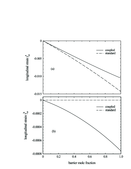
We consider a model SL consisting of 20Å N barriers and 60Å GaN wells on a GaN buffer. Assuming the pseudomorphic condition to hold, the GaN layers will have no in-plane strain components, while the AlGaN layers will have in-plane strains in accordance with Eq. (17). Using Eqs. (II.2), (II.2), and (II.2), the strain and electric fields are calculated for the fully-coupled model and compared with the standard results. Following established convention, a negative sign in the present calculations indicates contraction and a positive sign extension relative to the unstrained state. Figures 2(a) and (b) show the longitudinal strain in the barrier and well layers, respectively, as a function of the barrier mole fraction for the fully-coupled and standard cases. Despite due to the lattice matching condition, a non-zero occurs due to electromechanical coupling, as predicted in Eq. (9) and again in Eq. (II.2), and shown in Fig. 2(b). This strain is a near linear function of the Al fraction and, in this example, is about % for .
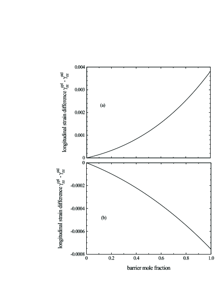
The largest strains occur in the AlGaN layers due to the lattice mismatch and it is also here that a significant deviation between the standard and fully-coupled models is seen as shown in Figs. 2(a) and (b). This deviation is shown in Figs. 3(a) and (b). The error of the standard model relative to the fully-coupled model can be in excess of 35% AlN/GaN SLs, as seen in this example. It is even higher in structures with higher electric fields in the barrier. This occurs when . For example, if we set =10Å and =60Å, the error for is about 45%. These deviations in the strain are quite significant and, as will be seen shortly, have an impact on the ISBT energies.
Figure 4 shows the calculated electric fields in the AlGaN and GaN layers for our model SL. From Eq. (II.2), it is seen that the larger electric field occurs in the thinner layer. The electric field calculated from the fully-coupled model is smaller in magnitude than the standard electric field due to an effective screening caused by the electromechanical coupling. This screening increases at higher strains. The deviation between the standard and fully-coupled electric fields is about 7% for .
Figure 5 shows the calculated ISBT energies between the first two electron subbands and the corresponding peak wavelengths for the model SL. The energies are calculated at , the location of the minimum energy separation between the first two subbands in the Brillouin zone. The present calculations show that there is little change in the energies between the zone center and zone boundary for a wide range of SLs. A number of factors contribute to the relatively narrow mini-bandwidth. First, the band edge discontinuity is quite large due to the large band gaps of the host materials. Second, the effective electron mass is large, in this case, in GaN and in AlN. Third, the built-in electric field causes the electron wave function to be localized in the triangular notch close to the AlGaN/GaN interface (see Fig. 1). All of these factors reduce the exponential tail of the electron wave functions between adjacent wells, which, in turn, would appear as a dispersion in the mini Brillouin zone. For some SLs, however, particularly those with thin wells, the wave functions will spread into the barrier layers, causing some dispersion in the Brillouin zone.
The most significant feature of Fig. 5 is the discrepancy between the standard and fully-coupled models. For example, for , the fully-coupled transition energy is lower than the standard value by 3.7 meV. This difference increases to 19.5 meV for . The latter result is especially significant, because high Al fractions are preferred for optical switching technology due to the shorter peak wavelength. The difference in energies between the two models is large enough to be measurable by, for example, Fourier-transform infrared spectroscopy (FTIR). The wavelength for the standard model is shorter by about 4% relative to the coupled model for .
The reason for the red shift of the fully-coupled results relative to the standard model can be understood by noting that the introduction of electromechanical coupling reduces the magnitude of the electric field (see Fig. 4). The smaller electric field results in a conduction band profile closer to flat-band conditions (see Fig. 1). In addition, a lowering of the effective barrier height occurs from the reduction of seen in Fig. 2. The more shallow triangular notch, together with a reduced barrier height, will cause the subbands to more closely spaced in energy. The calculated red shift of the ISBT is distinct from the Stark shift seen in interband transitions where the transition energy shifts to higher energy as the electric field is reduced.
III.2 Doped Superlattices
For optical switching technology, it is necessary to -dope the SL in order to populate the first electron subband to facilitate ISBTs. For such structures, we use the fully-coupled numerical model described previously. The model is tested against published optical data for various SL structures. Table 1 shows the calculated ISBT energy between the first two subbands for ten SL samples taken from the literature. The standard and fully-coupled results are contrasted. It is evident that two models give differing results. Also evident is the consistent red shift of the fully-coupled results compared to the standard results for the reasons discussed in Sec. III.1. The differences depend on the layer thicknesses and doping of the samples, varying from 4.9 meV for sample A to 19.4 meV for sample D. These differences are significant enough to be measurable by standard techniques such as FTIR.
Also shown in Table 1 are the experimentally-obtained peak wavelengths for the SLs. These are compared with the calculated wavelengths from the standard and fully-coupled models. Except for samples F and G, it is clear that the calculated wavelengths are in reasonably good agreement with the published data. The causes of the discrepancies for samples F and G are unclear at this point. It should be noted that we have not attempted to optimize the input parameters and have chosen instead to use a generic set of parametersJogai (2002) without fitting. The calculated results are very sensitive to all of the input parameters and also to the geometry and Al fraction. For instance, if the well thicknesses in samples F and G are increased by two monolayers and reduced to 0.6, the wavelength can be fitted to within 5% using the fully-coupled model. More precise modeling of optical data will be the subject of future work. For now, we simply wish to illustrate the importance of incorporating a fully-coupled strain model in the design of optical switches.
The calculations in Table 1 were done for a temperature of 300K. At 77K, there is a blue shift of the transition energies due to the slight increase in . The blue shift is largest for SLs with the thinnest wells wherein the subbands are pushed closer to band edge discontinuity and smallest for SLs with the thickest wells in which the first two subbands see less of the band edge discontinuity. For example, the shift is about 8.5 meV for sample A and about 0.15 meV for sample E.
Figure 6 shows the calculated conduction band edge and electron distribution for sample C in Table 1 using the fully-coupled model. Also shown are the Fermi energy and the first three electron subbands calculated at the Brillouin zone boundary. This profile was calculated at 300K. At 77K, there is no discernible change in the electron distribution function and the slope of the conduction band edge. There are, however, shifts in the subbands of a few meV depending on the structure, as described earlier. As the calculation shows, the Fermi energy appears slightly above the first subband but well below the second subband, in spite of the high doping, ensuring that the first subband is populated by electrons and the second nearly empty in order to facilitate optical absorption. This Fermi energy position is consistent with measured SL structures with transition energies corresponding to transitions. The calculated distribution and band edges, therefore, appear plausible.
Figure 7 shows the electric field distribution for selected structures from Table 1 using the fully-coupled model. The large electric fields in these structures are a consequence of the large polarization discontinuity across the interface. It is difficult to verify these fields directly. There is indirect evidence, however, that these fields are not unreasonable given the close fits of the ISBT wavelengths with experimental data. Due to the heavy doping, analytical expressions commonly used to estimate the electric fields would lead to errors, especially in the wells where the field is clearly non-linear. Even on the barrier side near the interface, there is an in increase in the magnitude of the field due to the penetration of the wave functions into the barrier. For such SLs, a numerical solution of the fully-coupled Poisson equation as describe here is essential.
IV Summary and conclusions
In summary, a fully-coupled model for the strain and the eigenstates of AlGaN/GaN polarization SLs has been presented. This model is compared with the standard strain model utilizing Hooke’s law. Both the spontaneous and piezoelectric polarizations are included, together with free electrons and ionic space charges. It is seen that the strain and electronic properties of the material are linked through the fully-coupled thermodynamic equation of state for piezoelectric materials. Separating the mechanical and electronic aspects of the SL in any theoretical modeling of the properties of these structures leads to errors in both the strain and the eigenstates of the system. For strongly coupled cases, such as AlGaN/GaN SLs, the corrections to the standard model can be significant. The ISBT energies calculated from the fully-coupled model show a measurable red shift compared to the corresponding energies calculated from the separable model. This result has consequences for the design of optical switches utilizing AlGaN/GaN SLs.
Acknowledgements.
The work of BJ was partially supported by the Air Force Office of Scientific Research (AFOSR) and performed at Air Force Research Laboratory, Materials and Manufacturing Directorate (AFRL/MLP), Wright Patterson Air Force Base under USAF Contract No. F33615-00-C-5402.References
- Suzuki and Iizuka (1997) N. Suzuki and N. Iizuka, Jpn. J. Appl. Phys. 36, L1006 (1997).
- Suzuki and Iizuka (1998) N. Suzuki and N. Iizuka, Jpn. J. Appl. Phys. 37, L369 (1998).
- Suzuki and Iizuka (1999) N. Suzuki and N. Iizuka, Jpn. J. Appl. Phys. 38, L363 (1999).
- Iizuka et al. (2000) N. Iizuka, K. Kaneko, N. Suzuki, T. Asano, S. Noda, and O. Wada, Appl. Phys. Lett. 77, 648 (2000).
- Heber et al. (2002) J. D. Heber, C. Gmachi, H. M. Ng, and A. Y. Cho, Appl. Phys. Lett. 81, 1237 (2002).
- Iizuka et al. (2002) N. Iizuka, K. Kaneko, and N. Suzuki, Appl. Phys. Lett. 81, 1803 (2002).
- Kishino et al. (2002) K. Kishino, A. Kikuchi, H. Kanazawa, and T. Tachibana, Appl. Phys. Lett. 81, 1234 (2002).
- Smith and Mailhiot (1990) D. L. Smith and C. Mailhiot, Rev. Mod. Phys. 62, 173 (1990).
- Löbl et al. (1999) H. P. Löbl, M. Klee, O. Wunnicke, R. Dekker, and E. v. Pelt, IEEE Ultrasonics Symposium 2, 1031 (1999).
- Naik et al. (2000) R. S. Naik, J. J. Lutsky, R. Reif, C. G. Sodini, A. Becker, L. Fetter, H. Huggins, R. Miller, J. Pastalan, G. Rittenhouse, et al., IEEE Trans. Ultrason. Ferroelectr. Freq. Control 47, 292 (2000).
- Cheng et al. (2001) C. C. Cheng, K. S. Kao, and Y. C. Chen, IEEE International Symposium on Applications of Ferroelectrics 1, 439 (2001).
- Palacios et al. (2002) T. Palacios, F. Calle, J. Grajal, M. Eickhoff, O. Ambacher, and C. Prieto, Materials Science and Engineering B 93, 154 (2002).
- Takagaki et al. (2002) Y. Takagaki, P. V. Santos, O. Brandt, H.-P. Schönherr, and K. H. Ploog, Phys. Rev. B 66, 155439 (2002).
- Zelenka (1986) J. Zelenka, Piezoelectric Resonators and their Applications, vol. 24 (Elsevier, Amsterdam, 1986).
- Auld (1990) B. A. Auld, Acoustic Fields and Waves in Solids, vol. I (Robert E. Krieger Publishing Company, Malabar, Florida, 1990).
- Jogai et al. (2003a) B. Jogai, J. D. Albrecht, and E. Pan, J. Appl. Phys. 94, 3984 (2003a).
- Jogai et al. (2003b) B. Jogai, J. D. Albrecht, and E. Pan, J. Appl. Phys. 94, 6566 (2003b).
- Nye (1985) J. F. Nye, Physical Properties of Crystals – Their representation by Tensors and Matrices (Clarendon Press, Oxford, 1985).
- (19) Ansi/ieee std 176-1987 ieee standard on piezoelectricity.
- Bernardini et al. (1997) F. Bernardini, V. Fiorentini, and D. Vanderbilt, Phys. Rev. B 56, R10024 (1997).
- Bahder (1995) T. B. Bahder, Phys. Rev. B 51, 10892 (1995).
- Gleize et al. (2001) J. Gleize, M. A. Renucci, and F. Bechstedt, Phys. Rev. B 63, 073308 (2001).
- Ridley et al. (2003) B. K. Ridley, W. J. Schaff, and L. F. Eastman, J. Appl. Phys. 94, 3972 (2003).
- Hedin and Lundqvist (1971) L. Hedin and B. I. Lundqvist, J. Phys. C 4, 2064 (1971).
- Jogai (2002) B. Jogai, Phys. Stat. Sol. (b) 233, 506 (2002).
- Bernardini and Fiorentini (2002) F. Bernardini and V. Fiorentini, Phys. Stat. Sol. (a) 190, 65 (2002).
| SL | (Å) | ||||||
|---|---|---|---|---|---|---|---|
| A111Ref. Iizuka et al., 2002, wells Si-doped . | 46/13 | 1 | 0.9521 | 0.9472 | 1.33 | 1.30 | 1.31 |
| B111Ref. Iizuka et al., 2002, wells Si-doped . | 46/18 | 1 | 0.9040 | 0.8930 | 1.48 | 1.37 | 1.39 |
| C111Ref. Iizuka et al., 2002, wells Si-doped . | 38/20 | 1 | 0.8610 | 0.8467 | 1.6 | 1.44 | 1.47 |
| D111Ref. Iizuka et al., 2002, wells Si-doped . | 46/33 | 1 | 0.7057 | 0.6863 | 1.85 | 1.76 | 1.81 |
| E111Ref. Iizuka et al., 2002, wells Si-doped . | 46/45 | 1 | 0.5800 | 0.5613 | 2.17 | 2.14 | 2.21 |
| F222Ref. Suzuki and Iizuka, 1999, wells Si-doped . | 30/30 | 0.65 | 0.4981 | 0.4879 | 3 | 2.49 | 2.55 |
| G222Ref. Suzuki and Iizuka, 1999, wells Si-doped . | 30/60 | 0.65 | 0.3740 | 0.3630 | 4 | 3.32 | 3.42 |
| H333Ref. Kishino et al., 2002, wells Si-doped . | 27.3/13.8 | 1 | 0.9809 | 0.9718 | 1.27 | 1.27 | 1.28 |
| I333Ref. Kishino et al., 2002, wells Si-doped . | 27.3/16.1 | 1 | 0.9352 | 0.9240 | 1.37 | 1.33 | 1.34 |
| J333Ref. Kishino et al., 2002, wells Si-doped . | 27.3/22.6 | 1 | 0.8052 | 0.7874 | 1.54 | 1.54 | 1.58 |