Abstract
The progress in investigation of two-band superconductor MgB2 by the point-contact spectroscopy (PCS) is given. Results of study of superconducting gap temperature and magnetic field dependence for two-dimensional and three-dimensional band and electron-phonon-interaction spectral function are presented. Correlation between the gap value and the intensity of the high Tc driving force – boron vibration mode, is provided. PCS data on some nonsuperconducting transition metal diborides are surveyed for comparison.
keywords:
point-contact spectroscopy, MgB2, two-band/gap superconductivity, electron-phonon interactionPoint-contact spectroscopy of two-band superconductor MgB2
1 Introduction
Magnesium diboride, like other diborides MeB2 (Me=Al, Zr, Ta, Nb, Ti, V etc.), crystalizes in a hexagonal structure, where honeycomb layers of boron are separated by magnesium ions located above and below the centers of boron hexagons. The hallmark of MgB2 is that it becomes superconducting (SC) at high critical temperature Tc ( 40 K) [1], which is a record breaking value among the s-p metals and alloys. The outstanding property of MgB2 is that this material represents a rare example of multi-band (2-D -band and 3-D -band) electronic structure, which are weakly connected with each other. These bands lead to very uncommon properties. For example, Tc almost does not depend on elastic scattering, unlike for other two-band superconductors [2]. The maximal upper critical magnetic field there can achieve a much higher value, than that for a one-band dirty superconductor [3]. The properties of MgB2 have been comprehensively calculated by the modern theoretical methods, which lead to principal understanding of their behavior in various experiments.
Electron band structure of MgB2 was calculated in very detail using different ab initio methods [4, 5, 6, 7, 8]. Topmost is that two filled incompletely bands have weak dispersion forming two nearly cylindrical sheets of the Fermi surface around A . Besides they retain their covalent structure representing unique case of conducting covalent bands which contribute to the strong electron-phonon coupling. Thus, the hole branch along A experiences huge interaction with phonon mode for carriers moving along plane, although its manifestation is screened effectively by the much faster hole mobility in -bands [2], which form two 3-D tubular network. Appropriate electron transport is very anisotropic ( [10]) with a plasma frequency (and Fermi velocity) for band along axis being an order of magnitude smaller than that in direction [11].
Inelastic -Ray scattering measurements [12] demonstrated a weakly dispersion branch between 60 and 70 meV in A direction with symmetry in point. The linewidth of this mode is about 2028 meV along A direction, while along M direction it is below the experimental resolution. This points to the very strong electron-phonon interaction (EPI) for this particular lattice vibration mode.
The SC energy gap distribution on the Fermi surface of MgB2 [13] shows maximum gap value along A direction which is due to very strong EPI. Just in this direction 2D band (cylinders along A direction) is located. The 3D band has much smaller EPI, and, correspondingly, the nearly 3 times smaller energy gap. In Ref. [13] it is shown that average value on band amounts up to . Moreover, can be decomposed between different phonon modes, and it appears that only E2g phonon mode along A direction plays a major role with a partial value of about [14], though concentrating in a very restricted phase space.
Driving mechanism for high in MgB2 is connected with the strong interaction between charge carriers and phonon modes, corresponding to antiparallel vibration of atoms in the boron planes. The electron band structure of MgB2 along A direction is such that the Fermi energy of hole carriers is only 0.5 eV, which shrinks even more while borons deviate from the equilibrium positions. Together with the 2D structure of the corresponding sheet of the Fermi surface, this leads to constant density of states at the Fermi energy and, correspondingly, to very strong EPI. Cappelluti et al. [15] point out that the small Fermi velocity for charge carriers along A direction leads to large nonadiabatic correction to (about twice as much compared with adiabatic Migdal-Eliashberg treatment). Although this interaction is a driving force to high in this compound, it does not lead to crystal structure instability, since it occupies only a small volume in the phase space.
According to theoretical models and bands in MgB2 are weakly connected. However, the energy gap of band goes to zero at the same as in the bulk, and correspondingly the , which is much less than the weak coupling BCS theory predicts. One can think of band as having intrinsically much lower K than the bulk [16] and at higher temperatures its superconductivity is induced by proximity effect in the k-space from band [17]. This proximity effect is very peculiar. From one side, this proximity is induced by the interband scattering between and sheets of the Fermi surface. On the other, the charge carriers connected with band are mainly located along the magnesium planes, which can be considered as a proximity effect in the coordinate space for alternating layers of structure, although at microscopically scale. Thus, MgB2 is a good example to study crossover between two-band superconductivity and simple proximity effect structure.
2 Samples and measurements
In this work the results for two kind of samples are surveyed. The first is thin c-axis oriented films with the thickness of about several hundreds of nanometer [18]. The residual resistance is about several tens of cm with residual resistance ratio (RRR) pointing out that films have a disorder between crystallites. It does not exclude that on some spots the films contain clean enough small single crystals on which we occasionally may fabricate a point contact (PC). Normally, the contacts were prepared by touching the film surface by noble metal counter electrode (Cu, Au, Ag) in the direction perpendicular to the substrate. Thus, nominally the preferential current direction in PC is along c axis. Nevertheless, since the surface of the films contains terraces with small crystallites, PC to ab plane of these crystallites is also possible.
The second type of samples are single crystals [19]. Crystals are plate-like (flakes) and have sub-millimeter size. They were glued by silver epoxy to the sample holder by one of their side faces. The opposite face of flakes was used as a ”needle” to gently touch the noble metal counter electrode in liquid helium. In this way we tried to make preferentially a contact along ab plane. In average, in the bulk, the single crystals are cleaner than the films, but one should be cautious, since the properties of the crystal surface differ from the properties of the bulk, and fabrication of PC may introduce uncontrolled further defects in the contact area.
Thus, a priori one cannot define the structure and composition of the obtained contacts. Nevertheless, much of that issue can be said by measuring various characteristics of a contact. Among those the most important is the Andreev-reflection-non-linearities of the curves in the SC energy-gap range. The magnetic field and temperature dependencies of the SC non-linearities supply us with additional information. And finally, much can be extracted from the nonlinearities in the normal state (so called, PC spectra). The more information about the electrical conductivity at different conditions of the particular contact we can collect, the more detailed and defined picture of it emerges. It is not an easy task, since a contact has a limited life time, due to electrical and mechanical shocks.
Let us give a rough estimation of the distance scales involved in the problem. The crystallite size of films is of the order of 100 nm (see [18]). The contact size in ballistic regime equals (the Sharvin formula). Taking cmcmcm2 [10], we obtain nm both along and directions for typical resistance of 10 . If we suppose that a grain is dirty (with very short mean free path), then we apply the Maxwell formula with the results for about 0.7 nm and 2.6 nm for and directions, respectively, taking for corresponding directions from the same reference [10]. Thus, the contact size can be of the order or smaller than the electronic mean free path ( nm and nm, according to [10]), which means that we are working in the spectroscopic regime, probing only a single grain.
Rowell [20], analyzing a big amount of experimental data for resistivity and its temperature dependence, came to the conclusion that for highly resistive samples only a small part of the effective cross section should be taken into account. The reason is that the grains in MgB2 are disconnected by oxide of magnesium and boron to great extent. For PCS previous analysis leads us to the conclusion that the contact resistance is frequently measured only for a single grain, either for several grains, with their intergrain boundaries facing the contact interface. This is due to the current spreading with the scale of the order of the contact size near the constriction.
3 Theoretical background of PCS
The non-linearities of the characteristic of a metallic contact, when one of the electrodes is in the SC state, can be written as [21]
| (1) |
Here is the contact resistance at zero bias in the normal state. is the backscattering inelastic current which depends on the electron mean free path (mfp) . For the ballistic contact this term amounts to
| (2) |
where is the inelastic electron mfp, and is the characteristic contact diameter. If the electron flow through the contact is diffusive (, being an elastic mfp) but still spectroscopic, since , then the expression (2) should be multiplied by . This decreases the characteristic size, where the inelastic scattering being essential, from to (), and for short makes the inelastic current very small. We notice that the inelastic backscattering current in the SC state is approximately equal to the same term in the normal state. Its second derivative turns out to be directly proportional to the EPI function [22, 23]
| (3) |
where describes the strength of the electron interaction with one or another phonon branch, stands for the phonon density of states. In PC spectra the EPI spectral function is modified by the transport factor, which increases strongly the backscattering processes contribution.
In the SC state the excess current (1), which is due to the Andreev reflection of electron quasiparticles from the boundary in a contact ( stands for ”constriction”), can be written as
| (4) |
where for ( being the SC energy gap).
Nonlinear term in the excess current (4) in its turn can be decomposed in two parts, which depend in a different way on the elastic scattering of electron quasiparticles:
| (5) |
where is of the order of , and . Notice, that the latter behaves very similar to the inelastic backscattering current , namely, it disappears if , while the first term in the right hand side of expression (5) does not depend in the first approximation on . This enables to distinguish elastic term from inelastic. Finally, all excess current terms disappear when destroying the superconductivity, while remains very similar in both SC and normal states.
From the expressions (1), (2), (4) and (5), it becomes clear that only on the relatively clean spots, one can observe the inelastic backscattering current provided the excess current term is negligible. The latter can be cancelled by suppression of superconductivity either with magnetic field or temperature. On the contrary, in the SC state, for dirty contacts, all the inelastic terms are very small, and the main non-linearity is provided by the -dependence of the excess current.
Brinkman et al. [11] have shown that even along ab-plane the contribution of band for MgB2 is less than that of band, to say nothing of the direction along c axis, where it is negligible small. The calculation predicts that if the ”tunneling cone” is about several degrees from precise ab plane, then two SC gaps should be visible in tunneling characteristics. In other directions only a single gap, corresponding to band, is visible. We will see below that this prediction is fulfilled in PC experiment, as well.
Even worse the things are when one tries to measure the anisotropic Eliashberg function by means of the SC tunneling. The single-band numerical inversion program gives non-certain results, as was shown in Ref. [25].
Point-contact spectroscopy in the normal state can help in this deadlock situation. It is known that the inelastic backscattering current is based on the same mechanism as an ordinary homogeneous resistance, provided the maximum energy of charge carriers is controlled by applied voltage. The electrical conductivity of MgB2 can be considered as parallel connections of two channels, corresponding to and bands [2]. The conductivity of band can be blocked by Mg-atoms disorder. This situation is already obtained in experiment, when the temperature coefficient of resistivity increases simultaneously with increase of residual resistivity, which leads to the violation of the Matthiessen’s rule (see Fig. 3 in [2]). In this case we obtain the direct access to -band conductivity, and the measurements of PC spectra of EPI for band are explicitly possible in the normal state. Below we will see that this unique situation happens in single crystals along ab plane.
4 Experimental results
4.1 Superconducting energy gaps
Typical shapes of with Andreev reflection features are shown in Fig. 4.1.
![[Uncaptioned image]](/html/cond-mat/0309693/assets/x1.png)
curves exhibit two sets of energy gap minima distributed as shown in Fig. 4.1 (upper panel), at 2.4 0.1 and 7.10.4 meV. These curves are nicely fitted by BTK [26] theory (with a small parameter) for two conducting channels with an adjusted gap weighting factor [27]. The second kind of represents only one gap structure and is better fitted with a single gap provided an increased depairing parameter (Fig. 4.1, inset). According to the calculation in [11] strong impurity scattering will cause the gaps to converge to 4.1 meV and to 25.4 K. Therefore the single gap spectra reflect a strong interband scattering due to impurities, which likely causes a ”semiconducting-like” behavior of above Tc. These two kinds of gap structure constitute about equal parts of a total number of about hundred junctions. Usually the contribution of the large gap in the double-gap spectra is an order of magnitude lower than that of the small one, which is in line with small contribution of band in conductivity along c axis [11].
![[Uncaptioned image]](/html/cond-mat/0309693/assets/x2.png)
In the lower panel of Fig. 4.1 the theoretical prediction of energy gap distribution [13] is shown. One can see that the theoretical positions of distribution maxima approximately coincide with the experimental values. Only the low-lying maximum is not seen in the experiment.
The same variety of energy gap structure is observed for single crystals as well, but with some peculiarity due to preferential orientation along ab plane. The most amazing of them is the observation of a gap structure in [37] with visually only the larger gap present. Such kind of spectra were not observed in thin films. It means that the conductivity is governed only by band. This may be caused that band is blocked completely by Mg disorder or by oxidation of Mg atoms on ab-side surface of the crystal. At the same time, in single crystal there is much less scattering in the boron planes, due to the robustness of B-B bonds. We will see below that just this case enables us to observe directly the most important phonon mode in the electron-phonon interaction within band.
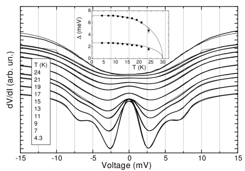
Figs. 1 and 2 display the series of temperature and magnetic field dependencies of the curves with their BTK fittings, respectively. Here, at low field (temperature) the two separate sets of the gap minima are clearly seen. The temperature dependence of both gaps follows the BCS prediction (see inset in Fig. 1). For temperatures above 25 K their behavior is unknown because this particular contact did not survive during the measurements likely due to thermal expansion of sample holder.
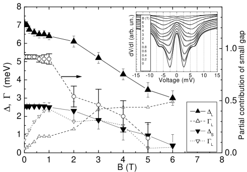
Fig. 2 shows magnetic field dependencies of large and small gaps. Surprisingly, the small gap value is not depressed by field about 1 T, and the estimated critical field about 6 T is much higher as stated in [28, 29], although the intensity of small gap minima is suppressed rapidly by a field about 1 T. Correspondingly, small gap contribution ( inversely depends on value, therefore nearly constant value between 0 and 1 T is due to the fact that rises by factor 4 at 1 T) to the spectra decreases by magnetic field significantly from 0.92 to 0.16 (see Fig. 2), while versus temperature even slightly increases from 0.92 at 4.3 K to 0.96 at 24 K (not shown). Theoretical investigation of the field dependence of maximum pair potential in two band superconductor MgB2 by Koshelev and Golubov [30] shows that for both gaps critical field is the same. Additionally, in recent experimental publication Bugoslavsky et al. [31] reported that both order parameters survive to a common magnetic field, while Gonnelli et al. [32] corrected their previous claims and mentioned that identification of magnetic field at which the band features in visually disappears with critical field for the bang might not be correct.
4.2 Electron-Phonon interaction
4.2.1 PC EPI spectra of non-SC diborides
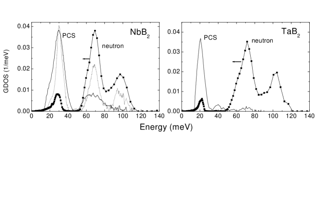
In Fig. 3 the PC EPI spectra (see also Eq. (3)) of non-SC diborides MeB2 (Me=Zr, Nb, Ta) [33] are shown. The cleanest sample we have is ZrB2 single crystal, and its PC EPI spectrum demonstrates more pronounced features (see Fig. 3, left panel). One recognizes a classical PC EPI spectrum from which one can estimate the position of 3 main phonon peaks (for ZrB2) and obtain the lower limit of the EPI parameter [33].
Essentially the similar spectra only with degradation of maxima with bias rise were observed for another diborides, taking into account their purity and increased EPI, which leads to the transition from spectroscopic to non-spectroscopic (thermal) regime of the current flow [33]. The positions of the low-energy peaks are proportional to the inverse square root of the masses of metals [33], as expected. For NbB2 and TaB2 the phonon density of states (DoS) is measured by means of neutron scattering [34]. The position of phonon peaks corresponds to the PC spectra maxima (Fig. 3). Because Nb and Zr have nearly the same atomic mass we suggest that they should have similar phonon DoS.
4.2.2 PC EPI spectra of MgB2 in c-oriented films
Unexpectedly, the stronger we suppress the superconductivity by magnetic field or temperature in MgB2, the less traces of phonon structure remain in the derivative [17]. This is in odd with the classical PCS, since the inelastic phonon spectrum should not depend on the state of electrodes in the first approximation (see section Theoretical background of PCS). Instead, most of the MgB2 spectra in the SC state show reproducible structure in the phonon energy range (Fig. 4) which was not similar to the expected phonon maxima superimposed on the rising background. This structure disappears by transition to the normal state. Quite interesting is that the intensity of this structure increases with increase of the value of the small gap, which means that the gap in band and observed phonon structure are connected [17]. Based on the theoretical consideration mentioned above, we conclude that the disorder in band is so strong that it precludes to observe the inelastic current, and the phonon non-linearities of excess current [17, 24] play the main role, which does not depend on the scattering.
Very rarely, we recovered (see [35]) the structure in which corresponds reasonably in shape to the phonon DoS (above 30 meV). Thus, for this contact we assumed to observe the inelastic PC spectrum for the band, which should be compared to the Eliashberg EPI function for the same band calculated in Ref. [36]. Both experimental spectrum and band Eliashberg function do not show the anomalously high intensity of phonon mode, since only the Eliashberg function for band is the principal driving force for high in MgB2. The same conclusion should be ascribed to the excess-current phonon structure, since it also corresponds to the band. This band has much larger Fermi velocity and plasma frequency along c-axis compared to band [11]. Thus, in order to register the principal EPI with phonon mode the PC spectra along ab plane should be measured.
4.2.3 PC EPI spectra in ab-direction
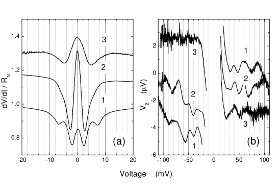
In Ref. [37] PC EPI spectra for single crystal oriented in ab plane were measured. As was mentioned above, the nominal orientation of the contact axis to be parallel to ab plane is not enough to be sure that this situation occurs in reality. Moreover, even if one establishes the necessary orientation (i.e., contact axis parallel to ab plane) the spectra should reflect both bands with the prevalence of undesired band, because due to spherical spreading of the current the orientational selectivity of the metallic PC is much worse than that for the plane tunnel junction, where it goes exponentially. The large mixture of -band contribution is clearly seen from the gap structure in Fig. 5 (b), inset. Beyond the wings at the biases corresponding to the large gap (supposed to belong to -band gap) the deep minima located at the smaller gap (correspondingly to -band gap) are clearly seen. The EPI spectrum of the same junction is shown in the main panel. One can see that the non-linearities of the characteristic at phonon biases are very small, and the reproducible structure roughly corresponding to the Eliashberg EPI function of the band [25, 36] appears in the bias range 20 60 mV. Above 60 mV PC spectrum broadens sufficiently sinking higher lying phonon maxima. No remarkable contribution of phonon mode is observed, like a big maximum of EPI at meV or a kink at for these biases.
Quite different spectrum is shown in Fig. 5(a), which is our key result. Consider first the characteristics (see inset). The energy gap structure shows gap minima corresponding to the large gap (-band gap). The increase of at larger biases is noticeably larger than in the previous case.
Before the saturation at biases meV, where the phonon DoS ends, the well resolved wide bump occurs in the PC spectrum, which is located at about 60 meV. Let us show that the bump is of spectroscopic origin, that is the regime of the current flow through the contact is not thermal, although the background at large biases ( meV) is high. To do so, we compare this bump with a PC spectrum in thermal regime for a model EPI function, which consists of Lorentzian at 60 meV with small (2 meV) width. Calculated according to Kulik [38], the thermal PC EPI spectrum, shown in Fig. 5(a) as a dashed line, is much broader.
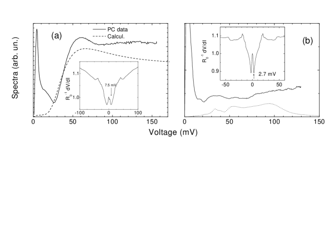
Any further increase of the width of the model spectra will widen the curve obtained. Comparing the experimental and model spectra enables us to conclude, that in spite of big width the maximum of experimental spectra is still correspond to the spectroscopic regime. Introducing greater disorder in the boron plane by fabrication procedure or by trying another spots on the side-face surface, the smeared thermal-like spectra were observed, coinciding in shape with the dashed curve in Fig. 5(a), which together with corresponding energy-gap structure can be ascribed to thermal limit mainly in band, despite the bath temperature is low enough.
PC spectrum with broad maxima including also one at about 60 mV were observed by [29] on polycrystalline MgB2 samples derived to the normal state by applying magnetic field and increasing of the temperature.
The big width of the EPI peak connected with phonon mode is not surprising. Shukla et al. [12] measured the phonon dispersion curves along A and M directions by means of inelastic X-ray scattering. The full width at half maximum for mode along A direction amounts to about 20-28 meV, which is well correspond to what we observe in PC spectrum. If the phonon life time corresponds to this (inverse) energy, then the phonon mean free path is about the lattice constant [37], and due to phonon reabsorption by nonequilibrium electrons, we should anticipate large background in the PC spectra as observed.
For a contact with E2g phonon modes in Fig. 5(a) the nonlinearity of the curves due to electron-phonon interaction can be estimated from the curves by about 10%. This is comparable with nonlinearity observed for non-SC diborides [33] with small electron-phonon coupling constant . The reason of relatively low nonlinearity of curves and small intensity of principal E2g phonon modes in spectra for MgB2 contacts can be the fact that anomalous strong interaction is characteristic for the restricted group of phonons with sufficiently small wave vector [9], whereas in PCS the large angle scattering is underlined.
5 Conclusions
Comprehensive PCS investigations of -axis oriented thin films and single crystals of MgB2 leads to the following conclusions:
-
•
The observed by Andreev reflection SC gaps in MgB2 are grouped at 2.4 and 7.0 meV and show basically a BCS-like temperature dependence. The two gap structure merges together in the case of strong elastic scattering remaining a single gap at about 3.5 meV.
-
•
Anomalous magnetic field dependencies of the gap structure in PCs reflect peculiarity of the two band structure of the SC order parameter in MgB2. In particular, small gap survives up to magnetic field close to the critical one for a large gap.
-
•
The phonon structure in the PC spectra of MgB2 can be revealed by: i) the inelastic backscattering current, like for ordinary PCS, and ii) by the energy dependence of the excess current. They can be discriminated after destroying superconductivity by magnetic filed or/and temperature, and varying electron mean free path.
-
•
The prevailing appearance in the PC spectra of boron mode, which mediates the creation of Cooper pairs, is seen for PC with a large gap that is along direction in accordance with the theory. The relatively small intensity of this mode in the PC spectra is likely due to their small wave vector and restricted phase volume.
-
•
Related diborides (ZrB2, NbB2, and TaB2) have PC spectra proportional to the electron-phonon-interaction spectral function, like in common metals and small EPI constant corresponding to their non-SC state at helium temperature.
Acknowledgements
The authors are grateful to N. L. Bobrov, P. N. Chubov, V. V. Fisun, O. E. Kvitnitskaya, L. V. Tyutrina for collaboration during MgB2 investigation and S.-I. Lee and S. Lee for samples providing. The work in Ukraine was supported by the State Foundation of Fundamental Research under Grant 7/528-2001.
References
- [1] J. Nagamatsu, N. Nakagawa, T. Muranaka, Y. Zenitani, J. Akimitsu, Nature 410, 63 (2001).
- [2] I.I. Mazin, O.K. Andersen, O. Jepsen, O.V. Dolgov, J. Kortus, A.A. Golubov, A.B. Kuz’menko, and D. van der Marel, Phys. Rev. Lett. 89, 107002 (2002).
- [3] A. Gurevich, Phys. Rev. B 67, 184514 (2003).
- [4] J.M. An and W.E. Pickett, Phys. Rev. Lett. 86, 4366 (2001).
- [5] Y. Kong, O.V. Dolgov, O. Jepsen, and O.K. Andersen, Phys. Rev. B 64, 020501(R) (2001).
- [6] J. Kortus, I.I. Mazin, K.D. Belashchenko, V.P. Antropov, and L.L. Boyer, Phys. Rev. Lett 86, 4656 (2001).
- [7] Amy Y. Liu, I.I. Mazin, and Jens Kortus, Phys. Rev. Lett. 87, 87005 (2001).
- [8] T. Yildirim, O. Gülseren, J.W. Lynn, C.M. Brown, T.J. Udovic, Q. Huang, N. Rogado, K.A. Regan, M.A. Hayward, J.S. Slusky, T. He, M. K. Haas, P. Khalifah, K. Inumaru, and R.J. Cava, Phys. Rev. Lett. 87, 037001 (2001).
- [9] I.I. Mazin, V.P. Antropov, Physica C 385, 49 (2003).
- [10] Yu. Eltsev, K. Nakao, S. Lee, T. Masui, N. Chikumoto, S. Tajima, N. Koshizuka, M. Murakami, Phys. Rev. B 66, 180504(R) (2002).
- [11] A. Brinkman, A.A. Golubov, H. Rogalla, O.V. Dolgov, J. Kortus, Y. Kong, O. Jepsen, and O.K. Andersen, Phys. Rev. B 65, 180517 (2002).
- [12] A. Shukla, M. Calandra, M. d’Astuto, M. Lazzeri, F. Mauri, Ch. Bellin, M. Krisch, J. Karpinski, S.M. Kazakov, J. Jun, D. Daghero, and K. Parlinski, Phys. Rev. Lett. 90, 095506 (2003).
- [13] Hyoung Joon Choi, David Roundy, Hong Sun, Marvin L. Cohen, Steven G. Louie, Nature 418, 758 (2002); Phys. Rev. B 66, 020513(R) (2002).
- [14] J.M. An, S.Y. Savrasov, H. Rosner, and W.E. Pickett, Phys. Rev. B 66, 220502(R) (2002).
- [15] E. Cappelluti, S. Ciuchi, C. Grimaldi, L. Pietronero, and S. Strässler, Phys. Rev. Lett. 88, 117003 (2002).
- [16] F. Bouquet ,Y. Wang, I. Sheikin, P. Toulemonde, M. Eisterer, H.W. Weber, S. Lee, S. Tajima, A. Junod, Physica C 385, 192 (2003).
- [17] I.K. Yanson, V.V. Fisun, N.L. Bobrov, Yu.G. Naidyuk, W.N. Kang, Eun-Mi Choi, Hyun-Jung Kim, and Sung-Ik Lee, Phys. Rev. B 67, 024517 (2003).
- [18] W.N.Kang, Eun-Mi Choi, Hyeong-Jin Kim, Hyun-Jung Kim, Sung-Ik Lee, Physica C 385, 24 (2003).
- [19] Sergey Lee, Physica C 385, 31 41 (2003); S. Lee, H. Mori, T. Masui, Yu. Eltsev, A. Yamanoto and S. Tajima, J. Phys. Soc. of Japan, 70, 2255 (2001).
- [20] J.M. Rowell, Supercond. Sci. Technol. 16, R17-27 (2003).
- [21] V.A. Khlus and A.N. Omel’yanchuk, Sov. J. Low Temp. Phys. 9, 189 (1983); V.A. Khlus, Sov. J. Low Temp. Phys. 9, 510 (1983).
- [22] I.O. Kulik, A.N. Omelyanchouk, and R.I. Shekhter, Sov. J. Low Temp. Phys. 3, 840 (1977).
- [23] I.K. Yanson, in book I.O. Kulik and R.Ellialtioglu (eds.), Quantum Mesoscopic Phenomena and Mesoscopic Devices in Microelectronic,, (Kluwer Acad. Publ., 2000) p. 61-77. (see also: cond-mat/0008116).
- [24] A.N. Omel’yanchuk, S.I. Beloborod’ko, and I.O. Kulik, Sov. J. Low Temp. Phys. 14, 630 (1988).
- [25] O.V. Dolgov, R.S. Gonnelli, G.A. Ummarino, A.A. Golubov, S.V. Shulga, and J. Kortus, cond-mat/0301542.
- [26] G.E. Blonder, M. Tinkham and T.M. Klapwijk, Phys. Rev. B 25, 4515 (1982).
- [27] Yu.G. Naidyuk, I.K. Yanson, L.V. Tyutrina, N.L. Bobrov, P.N. Chubov, W.N. Kang, Hyeong-Jin Kim, Eun-Mi Choi, and Sung-Ik Lee, JETP Lett. 75, 283 (2002).
- [28] R.S. Gonnelli, D. Daghero, G.A. Ummarino, V.A. Stepanov, J. Jun, S.M. Kazakov and J. Karpinski, Phys. Rev. Lett. 89 247004 (2002).
- [29] P. Samuely, P. Szabo, J. Kacmarcik, T. Klein, A.G.M. Jansen, Physica C 385 244 (2003).
- [30] A. E. Koshelev and A. A. Golubov, Phys. Rev. Lett. 90, 177002 (2003).
- [31] Y.Bugoslavsky, Y.Miyoshi, G.K. Perkins, A.D. Caplin, L.F.Cohen, A.V. Pogrebnyakov, X.X. Xi, cond-mat/0307540.
- [32] R.S. Gonnelli, D. Daghero, G.A. Ummarino, V. Dellarocca, V.A. Stepanov, J. Jun, S.M. Kazakov and J. Karpinski, cond-mat/0308152.
- [33] Yu.G. Naidyuk, O.E. Kvitnitskaya, I.K. Yanson, S.-L. Drechsler, G. Behr, and S. Otani, Phys. Rev. B 66, 140301 (2002).
- [34] R. Heid, B. Renker, H. Schober, P. Adelmann, D. Ernst, and K.-P. Bohnen, Phys. Phys. B 67, 180510(R)(2003).
- [35] N.L. Bobrov, P.N. Chubov, Yu.G. Naidyuk, L.V. Tyutrina, I.K. Yanson, W.N. Kang, Hyeong-Jin Kim, Eun-Mi Choi, C.U. Jung, and Sung-Ik Lee, in book New Trends in Superconductivty, Vol.67 of NATO Science Series II: Math. Phys. and Chem., ed. by J. F. Annett and S. Kruchinin, (Kluwer Acad. Publ., 2002), p.225.
- [36] A.A. Golubov, J. Kortus, O.V. Dolgov, O. Jepsen, Y. Kong, O.K. Andersen, B.J. Gibson, K. Ahn, and R.K. Kremer, J. Phys.: Condens. Matter 14, 1353 (2002).
- [37] Yu.G. Naidyuk, I.K. Yanson, O.E. Kvitnitskaya, S. Lee, and S. Tajima, Phys. Rev. Lett., 90, 197001 (2003).
- [38] I.O. Kulik, Sov. J. Low Temp. Phys. 18, 302 (1992).