Experimental demonstration of photonic crystal waveplates
Abstract
We have constructed and experimentally tested a microwave half waveplate using the dispersive birefringent properties of a bulk two-dimensional photonic crystal away from its band gap. Our waveplate device exhibited a 200:1 polarization contrast, limited by our experimental resolution. We anticipate that photonic crystal waveplates will have important practical applications in several areas, including integrated photonic circuits.
pacs:
42.25.Ja, 42.25.Lc, 42.70.Qs, 78.20.Fm, 41.20.JbPhotonic crystals are passive, usually dielectric, periodic structures capable of producing distinctive reflected and transmitted fields from impinging electromagnetic (EM) waves Yablonovitch1989 . These structures are known to selectively forbid the propagation of light within certain frequency and wavevector bands through interference between multiple Bragg reflections Chow2000 ; Hickmann2002 . This phenomenon has been described as a photonic band gap in analogy with the electronic band structures of solid state materials. Although this analogy is relevant, the scalar approximation used for electronic theory neglects polarization effects, associated with the vector fields of electromagnetic waves, essential for photonic crystals. Here we explore some polarization-dependent effects of photonic crystal structures.
Photonic band gap structures can, in principle, be constructed in essentially any geometry with periodicity in one, two, or all three dimensions. Unfortunately, fabrication difficulties increase substantially as the dimensionality of the periodicity is increased. Among the wide variety of possible applications based on the band structure of photonic crystals are novel waveguides Cregan1999 and the suppression of spontaneous emission, leading to the possibility of thresholdless lasers Yablonovitch1987 . In addition to the well-known intensity effects, it has also been shown that photonic crystals have a nontrivial effect on the phase of EM waves in the band gap Hache2002 ; Solli2002 .
Although the band gap characteristics of photonic crystals have received significant attention, their transmission and especially phase effects in transparent spectral regions have been much less studied. Furthermore, there has been relatively little attention paid to birefringent polarization effects associated with photonic crystals. Most of the existing experimental and theoretical work in this area has been confined to studies of polarization behavior in photonic band gap waveguides Ortigosa-Blanch2000 ; Hansen2001 ; Kerbage2002 or in photonic crystal lasing cavities Noda2001 . There has also been some theoretical and experimental investigation of polarization and birefringence in nonlinear fiber Bragg gratings Slusher2000 ; Pereira2002 . To date, the polarization properties of two-dimensional photonic crystals have been discussed only once Li2001 , in a paper theoretically predicting the birefringent behavior characteristic of a waveplate.
It is possible to understand the existence of birefringence in a bulk 2D photonic crystal based on the anisotropy of the structure. A bulk 2D crystal is one in which the extruded (nonperiodic) dimension is much longer than the lattice constant. Since the dielectric interfaces are curved, the Fresnel coefficients for the two possible polarizations are different at normal incidence, being cumulative for multiple interfaces. An alternative explanation is found by considering the transmission characteristics of the structure. In particular, it has already been shown that the amplitude transmission of an EM wave through a bulk 2D photonic crystal is polarization-dependent in the band gap region; the center frequency, depth, and spectral width of the band gap depend on the polarization Hickmann2002 . Furthermore, it is well known that the absorption lines of a dissipative EM system can have effects on the phases of transmitted waves, even for frequencies away from the absorptive spectral regions Jackson1999 . Although dielectric photonic crystals are dissipationless, the band gaps should create similar dispersive effects, even in transparent spectral regions Ditchburn1976 ; Kittel1996 . Since bulk 2D photonic crystals have well-defined, but characteristically different band gap properties for waves of different polarizations, they should also possess birefringent phase delay properties (i.e., indices of refraction) in transparent spectral regions. In fact, significant phase birefringence has already been reported within the band gap of a bulk 2D photonic crystal Solli2002 .
Since Maxwell’s equations are scale-invariant, all results presented here apply across the electromagnetic spectrum. Photonic crystal birefringence should enable the construction of waveplates in all regions of the EM spectrum. Particularly in the optical region, this large birefringence could lead to much more compact waveplates than are currently available. It may also have important applications in photonic crystal circuits, integrated nonlinear optical systems based on selectively-defective periodic dielectric structures which have been proposed as all-optical switches Mingaleev2002 . One could imagine highly integrable and compact photonic-crystal circuit elements such as polarization discriminators, polarizing beamsplitters and even optical diodes, based on photonic crystal waveplates.
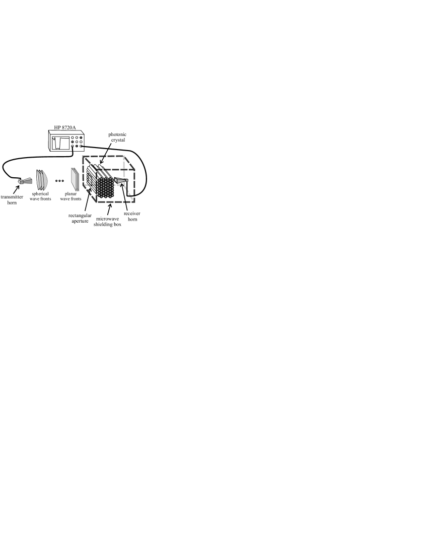
In this work, we report the experimental demonstration of a bulk two-dimensional (2D) photonic crystal waveplate. We have observed a relatively simple photonic band gap structure controllably rotate the angle of the plane of polarization of an incident linearly polarized EM wave. The photonic crystals used in this experiment were fabricated using a method that we have previously described Hickmann2002 . In summary, we stack hollow acrylic pipes in a hexagonal array, and cement them together with an acrylic solvent glue. The pipes used to construct the crystals used in this experiment have an outer diameter of 1/2 inch, and the final structures have air-filling fractions of 0.60. We tested crystals ranging from two to twenty layers of acrylic pipes. The microwave wavelength scale of these systems means that we can fabricate high-quality crystals relatively easily.
Our transmission measurement procedure has also been described elsewhere Hickmann2002 . Microwaves are broadcast from an HP 8720A vector network analyzer (VNA) and coupled into free space with a polarization-sensitive antenna (horn). The crystal and receiver horn (also polarization-sensitive) are placed inside a microwave-shielded box 1.6 m away with an aperture 14 cm 17 cm. These distances are chosen so that the microwaves arriving at the crystal are effectively plane waves with a well-defined linear polarization. The crystal is oriented so that the microwaves are incident in the direction Foteinopoulou2001 . A schematic of the experimental setup is presented in Fig. 1.
We have observed a clean exponential formation of the band gap in this crystal with increasing number of layers Hickmann2002 . The band gap center frequency is roughly 11 GHz for transverse magnetic (TM) waves and 10.5 GHz for transverse electric (TE) waves. The band gap depth and width also depend on polarization. We label the polarizations TE (TM) for the case in which the electric field is perpendicular (parallel) to the plane of symmetry of the crystal.
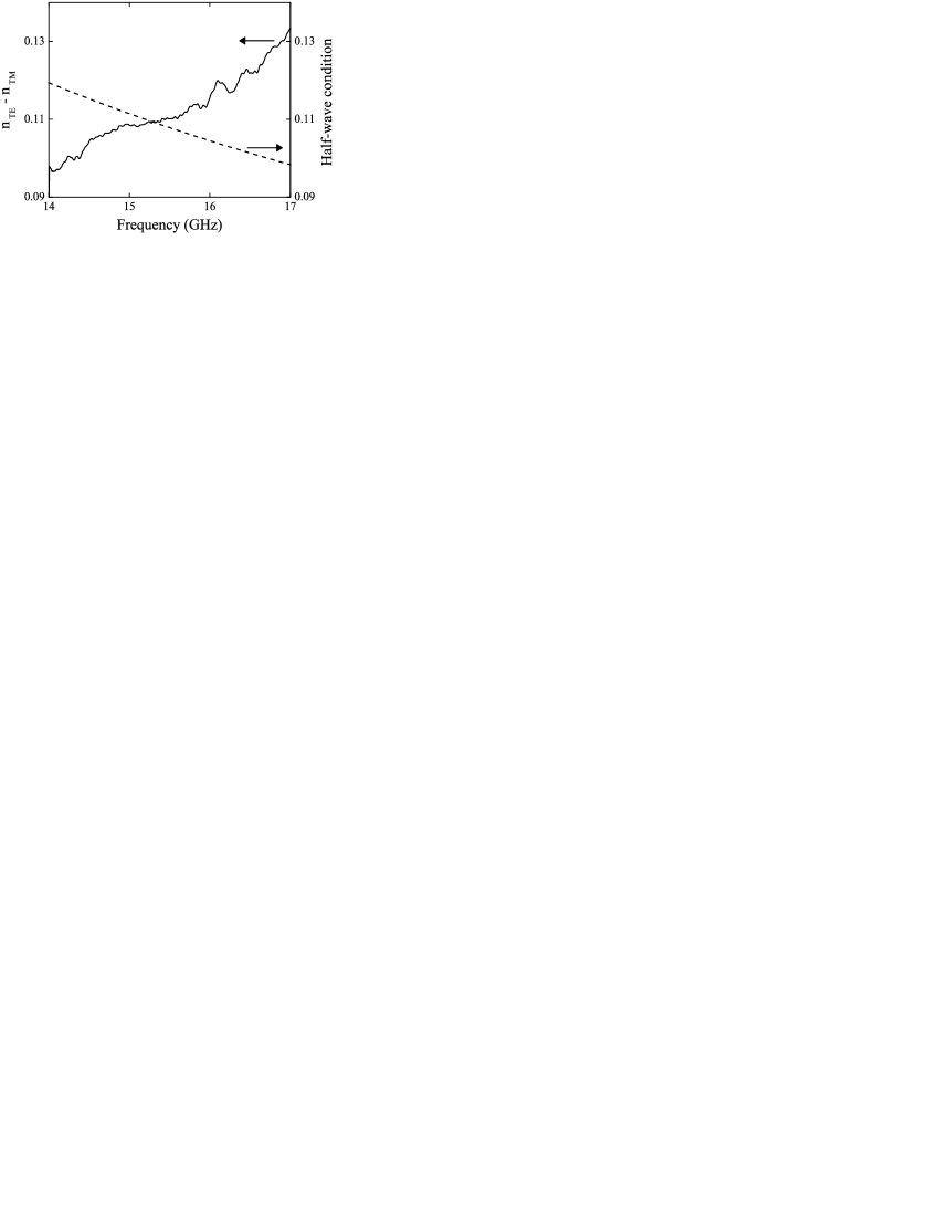
The vector capability of the network analyzer allows us to measure both transmission and phase delay of the microwaves at the receiver horn. We initially measured the phase delay in the frequency region of 14 to 20 GHz. With a simple model of the relation between phase delay and the index of refraction Solli2002 , we calculated the index of refraction for both polarizations of incident microwaves, where is the angular frequency. For a large range of frequencies (including frequencies far from the band gap), the two polarizations experience significantly different values of (see Fig. 2), demonstrating birefringence and suggesting that this photonic crystal will behave as a waveplate for a particular frequency range.
For a given value of , a zero-order half waveplate shifts the relative phase of the TE and TM polarizations by , leading to the relation
| (1) |
where L is the crystal length. Eq. 1 and the data from Fig. 2 indicate that our eight-layer crystal will act as a half waveplate for microwaves at 15.3 GHz. To demonstrate this, we first confirmed that our horns transmitted and received a single well-defined linear polarization of the electric field; for crossed transmitter and receiver horns, the power transmission was suppressed by 35 dB relative to the aligned configuration.
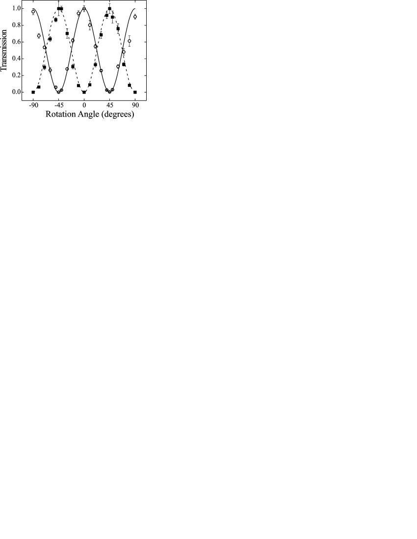
Next we recorded the power transmission through the crystal averaged over 15.2-15.4 GHz, as it was rotated through about the axis of optical propagation (Fig. 3). For both crossed (solid squares) and aligned (open circles) transmitting and receiving horns, the results show a clear squared-sinusoid (Malus) law for the transmitted power, with the correct period for a half waveplate. In Fig. 3, we have also plotted the functions (solid line) and (dashed line), which fit the experimental data extremely well without the adjustment of any parameter. Since Malus’ law holds for both horn configurations, this effect is clearly due to polarization rotation and not to an overall drop in transmission through the crystal. The polarization contrast is better than 200:1 (limited by the experimental resolution of our setup), indicating that the linear polarization is not degraded by the crystal.
In conclusion, we have presented the first experimental demonstration of a photonic crystal waveplate, able to rotate linear polarizations through arbitrary angles. Any photonic crystal whose band gap properties depend on polarization should exhibit some type of birefringence. Furthermore, it should be possible to engineer or tailor the birefringence by tuning to different transparent frequency bands and/or modifying the relative properties of the band gaps by changing the filling fraction, lattice spacing, dielectric composition, or structure geometry. We anticipate that this type of birefringent behavior in photonic crystals will have significant applicability, particularly at optical wavelengths in integrated photonic circuits.
This work was supported by ARO grant number DAAD19-02-1-0276. We thank the UC Berkeley Astronomy Department, in particular Dr. R. Plambeck, for lending us the VNA. JMH thanks the support from Instituto do Milênio de Informação Quântica, CAPES, CNPq, FAPEAL, PRONEX-NEON, ANP-CTPETRO.
References
- (1) E. Yablonovich and T. J. Gmitter, Phys. Rev. Lett. 63, 1950 (1989); E. Yablonovitch, Sci. Am. 285 (6), 46 (December 2001).
- (2) E. Chow, S. Y. Lin, S. G. Johnson, P. R. Villeneuve, J. D. Joannopoulos, J. R. Wendt, G. A. Vawter, W. Zubrzycki, H. Hou, and A. Alleman, Nature 407, 983 (2000).
- (3) J. M. Hickmann, D. Solli, C. F. McCormick, R. Plambeck, and R. Y. Chiao, J. Appl. Phys. 12, 6918 (2002).
- (4) R. F. Cregan, B. J. Mangan, J. C. Knight, T. A. Birks, P. St. J. Russell, P. J. Roberts, D. C. Allan, Science 285, 1537 (1999).
- (5) E. Yablonovitch, Phys. Rev. Lett. 58, 2059-2062 (1987).
- (6) A. Haché and L. Poirier, Appl. Phys. Lett. 80, 518 (2002).
- (7) D. R. Solli, C. F. McCormick, R. Y. Chiao, and J. M. Hickmann, to appear in IEEE Journal of Selected Topics in Quantum Electronics (2003).
- (8) A. Ortigosa-Blanch, J. C. Knight, W. J. Wadsworth, J. Arriaga, B. J. Mangan, T. A. Birks, and P. St. J. Russell, Opt. Lett. 25, 1325 (2000).
- (9) T. P. Hansen, J. Broeng, S. E. B. Libori, E. Knudsen, A. Bjarklev, J. R. Jensen, and H. Simonsen, IEEE Phot. Tech. Lett. 13, 588 (2001).
- (10) C. Kerbage, P. Steinvurzel, P. Reyes, P. S. Westbrook, R. S. Windeler, A. Hale, and B. J. Eggleton, Opt. Lett. 27, 842 (2002).
- (11) S. Noda, M. Yokoyama, M. Imada, A. Chutinan, and M. Mochizuki, Science 293, 1123 (2001).
- (12) R. E. Slusher, S. Spalter, B. J. Eggleton, S. Pereira, and J. E. Sipe, Opt. Lett. 25, 749 (2000).
- (13) S. Pereira, J. E. Sipe, R. E. Slusher, and Stefan Spälter, J. Opt. Soc. Am. B 19, 1509 (2002).
- (14) L. Li, Appl. Phys. Lett. 78, 3400 (2001).
- (15) See, for example, J. D. Jackson, Classical Electrodynamics, 3rd ed., (Wiley, New York, 1999), Chap. 7.
- (16) R. W. Ditchburn, Light, 3rd ed., (Interscience, New York, 1976), Appendix XIX B.
- (17) C. Kittel, Introduction to Solid State Physics, 7th ed., (Wiley, New York, 1996), Chap. 11.
- (18) S. Mingaleev and Y. Kivshar, Opt. & Phot. News 13, 48 (2002).
- (19) S. Foteinopoulou, A. Rosenberg, M. M. Sigalas and C. M. Soukoulis, J. Appl. Phys. 89, 824 (2001).