Heteroepitaxial growth of high-K gate oxides on silicon: insights from first-principles calculations on Zr on Si(001)
Abstract
Metal deposition of Zr an a Si(001) surface has been studied by state-of-the-art electronic structure calculations. The energy per Zr adatom as a function of the coverage shows, that Zr forms silicide islands even at low coverages. Adsorbed Zr is thermodynamically unstable against the formation of bulk silicide ZrSi2. The observation that the islands consist of structural elements of the bulk silicide is an indication that silicide grains will form spontaneously.
pacs:
82.65.F, 31.15.A, 68.55I Introduction
The scaling of the CMOS transistor has been the driving force behind the tremendous increase in microprocessor performance observed during the last decades. While the problems of the past were dominated by manufactural aspects, one now faces the first fundamental physical limitations as structures in logical devices approach atomic dimensions.
As a rule of thumb, the thickness of the gate-oxide has to be directly proportional to the channel length in a MOSFET (metal oxide silicon field effect transistor) device. In the course of the ongoing miniaturization, also the thickness of this insulating layer is being continually reduced. By the year 2007, gate-oxides in a transistor will approach a thickness of 1.5 nmroadmap , which corresponds to about ten typical atomic distances. The quantum mechanical tunneling currents through such a thin oxide are intolerable, and cause increased power consumption and deteriorated switching characteristics of the transistor. Replacing SiO2-based oxides, nowadays employed as gate dielectric, is one of the “key challenges” to the semiconductor industryroadmap , which has to find a solution within the next 4 to 5 years.
Employing high-k ( large dielectric constant) oxides would allow for a greater physical thickness while preserving the electrical properties. Possible candidates have to meet an extensive list of requirementswil01 such as sufficiently large band offsets, thermodynamical stability or interface quality.
The Si–SiO2 system meets all these requirements in an unparallelized waybuc00 . First attempts to grow alternative oxides on Si(001) did not yield satisfactory results for a variety of reasons – often originating in the interface region.
In the course of changing to a new gate material, one also considers to now grow crystalline oxide layers. It has been a paradigm that the gate oxide must be amorphous in order to avoid dislocations and grain boundaries, which provide natural pathways for leakage currents and atom diffusion. However, in the very small devices used in the near future, the probability for such a defect may be sufficiently small. On the other hand, epitaxial oxides bear the promise of very low defect concentrations at the interface to silicon, which is crucial for efficient device operation.
The first account of heteroepitaxial growth of a transition metal oxide has been presented by a seminal work of McKeemck01 who succeeded in growing SrTiO3 on Si(001). For the divalent elements detailed studies have been performedyao99 ; oji01 ; her00 ; bak96 ; fan90 ; wan99 . As similar understanding does not yet exist for the technological relevant early transition metals such as Zirconium. Theoretical studies on Zr are limited bulk interface calculations of silicateskaw01 .
The deposition and formation of an interface between one of the major contenders for high-k oxides, namely Zirconia (ZrO2), and silicon has not yet been investigated with ab-initio simulations. As a first step we performed state-of-the-art electronic structure calculations of the deposition of Zr on Si(001) up to a coverage of two monolayers (ML).
II Computational Aspects
We performed first-principles calculations within the framework of density functional theorydft1 ; dft2 using the gradient corrected density functional of Perdew, Burke and Enzerhofpbe . The electronic structure problem has been solved with the projector augmented waves methodblo94 , which uses augmented plane waves to describe the full wave-functions and densities without shape approximation. The PAW method as implemented in the CP-PAW code employs the Car-Parrinello approachcpmd to minimize the total energy functional.
The core electrons are described within the frozen core approximation with the semi-core (4 and 4) shells of the Zr atoms treated as valence electrons. Plane wave cutoffs of 30 and 60 Ry for the wave functions and the density have been used.
For metallic system we minimized the Mermin functional with respect to the occupation numbers which yields the Fermi-Dirac distribution for the electrons. An electronic temperature of 1000 K was used. The zero-Kelvin result has been extrapolated using the method suggested by sch97 .
The reconstructed Si(001) surface is the template for our growth studies. It is modeled by a slab consisting of 5 silicon layers, where the bottom layer is saturated with two hydrogen atoms per silicon. The position of the hydrogen atoms and the lowest silicon layer has been frozen. Supercells with 16 atoms per layer have been used for the calculations of Zr in the dilute limit, 8 atoms per layer for all higher coverages. In the first case, the distance between two periodic images of an adatom is 15.36 Å. For all surface calculations the k-mesh density corresponds to 64 lateral k-points per surface unit cell.
III Dilute Limit
Fig. 1. shows the structure of the reconstructed Si(001) surface. Excellent accounts covering the full complexity of the surface reconstruction can be found in literaturecha79 ; sch01 . The resulting structure can, however, be explained by the following considerations: While every bulk silicon is 4-fold coordinated, the surface atoms lack their upper bonding partners which leaves 2 dangling bonds per atom, each occupied by one electron. In a first step, two neighboring silicon atoms form a dimer bond – initially parallel to the surface – which leaves one dangling bond per atom. Now both electrons are transferred into one dangling bond to reduce the number of unpaired electrons to zero. This results in the buckling as the silicon with the filled dangling bond prefers a tetrahedral bonding arrangement, while the other prefers a planar sp2 configuration. From the electrostatic point of view, the alternating buckling behavior is favorable. Our calculations readily reproduce previously reported results such as the reconstruction and the difference in -coordinate of two silicon atoms within a dimernor93 .
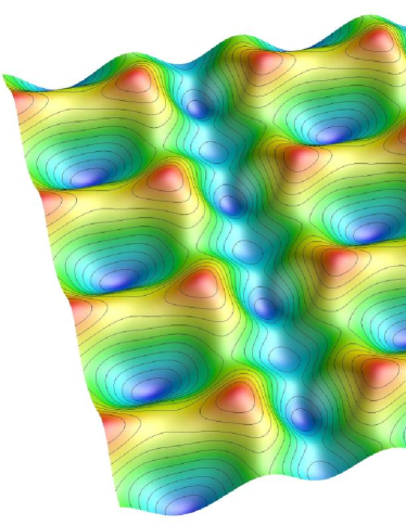
The energy surface of a Zr adatom on Si(001), has been obtained by freezing the lateral position of the adsorbed atom relative to the slab backplane, while all other degrees of freedom were fully relaxed. We used a grid of twelve Zr positions in the irreducible zone of the reconstructed silicon surface.
The resulting total energy surface for an isolated Zr on top of Si(001) is shown in Fig. 2. Two nearly degenerate positions can be identified. One is located in the valley right in the middle of two dimers of neighboring rows and the other on top of a dimer row between to adjacent dimers. A third, local minimum, is located in the valley and has an energy 0.30 eV higher relative to the most favorable positions. The diffusion is quasi one-dimensional with barriers of 0.70 eV for diffusion parallel to the dimer rows and 1.63 eV from the valley to the row.
IV Coverage of 0.25 and 0.5 Monolayers
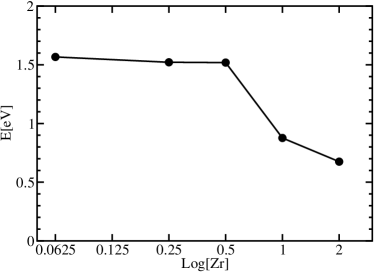
In order to investigate the formation of a continuous film, we increased the coverage. The structures with coverages of 0.25 ML and 0.5 ML have similar energies per Zr atom as the dilute limit (see Fig. 3). A wealth of complex structures has been found. Here, however, we only summarize the main trends of the chemical binding.
To first approximation Zr prefers a formal 4+ charge state – the projected density of states of the Zr -states is located well above the Fermi level. It is well known that for transition metal cations the -and -electrons are located above the -states, and have only a minor effect on the occupied states. The silicon dimers at the surface accept up to two electrons in their dangling bonds. A clear structural indication that the dangling bonds are filled is the disappearance of the dimer buckling.
Further electrons that are supplied at increased coverage of Zr, occupy the antibonding states of the dimer bond. As a consequence the silicon dimers break up. This happens at a coverage of half a ML and above. It should be noted, however, that metallic states accept some of the electrons so that the number of broken dimers does not directly correlate with the number of Zr adatoms in the ratio one to one. As a result of the interplay between breaking dimers and metallic states we find fairly complex reconstructions of the surface structure for intermediate coverages.
V Silicide Formation
Upon increase of the coverage to a full ML, the energy drops by 0.64 eV per adatom (see Fig. 3). The stable structure with ML coverage is shown in Fig. 4. All dimer bonds of the surface layer are broken, and the Zr atoms occupy the centers of the square array of surface silicon atoms in the resulting reconstruction. Such a layer is one structural element of bulk ZrSi2.
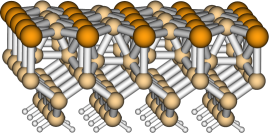
The energy gain is, however, not due to the surface geometry but can be attributed to a dimer reconstruction of the silicon subsurface. A metastable state without this reconstruction is even higher in energy than adsorbed Zr at lower coverages.
During the reconstruction, the silicon atoms in the layer underneath the ZrSi surface layer form dimers analogous to the bare silicon surface. In contrast to the dimer row reconstruction of the silicon surface, these subsurface dimers are not buckled and are arranged in a checkerboard instead of a row pattern.
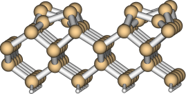
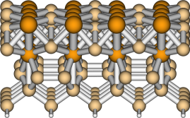
At a coverage of two MLs a second ZrSi layer is formed. This configuration is shown in Fig. 5. The second layer is nearly identical to the first, but is shifted laterally. The double layer is again a structural element of bulk ZrSi2, the structure of which is shown in Fig. 6. The ZrSi double layer consists of one-dimensional Si zig-zag chains separated by Zr atoms. The Zr atoms lie approximately in the plane of the upper and lower atoms of the Si chain. As for ML coverage the first silicon layer underneath the ZrSi double layer exhibits a dimer reconstruction.

Despite an additional energy gain from the ML coverage to a coverage of two MLs of 0.25 eV per adatom, even this structure is still 0.67 eV higher in energy than bulk ZrSi2. While the atomic process has not yet been resolved in every detail, our findings give strong indications for the nucleation of the silicide.
VI Discussion and Conclusion
We presented the results of state of the art ab-inito electronic structure calculations aiming at understanding the deposition of Zr atoms on a Si(001) surface as it is the case in an MBE reaction chamber.
Our results are summarized in Fig. 3, which shows the energy per Zr adatom as a function of the coverage. For coverages below one monolayer the the energy is nearly independent of the coverage. At a coverage of 1 ML we observe a sharp drop in energy by 0.64 eV, followed by further drops in energy for higher coverages. All structures are less stable than bulk silicide.
Our findings suggest that islands with a local coverage of 1 ML or higher are formed even at low coverages. The islands contain structural elements of bulk ZrSi2, which is more stable than any surface structure. Therefore a likely scenario is the formation of bulk silicide grains, that disrupt the surface morphology, and are detrimental for epitaxial growth. Modification of growth conditions, such as exposing the surface to a oxygen containing ambient, may bypass silicide formation during the first growth steps.
Acknowledgments
This work has been funded by the European Commission in the project ”INVEST” (Integration of Very High-k Dielectrics with CMOS Technology) IST-2000-28495 and by the AURORA project (SBF F011) of the Austrian Science Fond. This work has benefited from the collaborations within the ESF Programme on ’Electronic Structure Calculations for Elucidating the Complex Atomistic Behavior of Solids and Surfaces’.
References
- [1] International Technology Roadmap for Semiconductors, 2001 Ed. http://public.itrs.net/.
- [2] G.D. Wilk, R.M. Wallace and J.M. Anthony, J. Appl. Phys 89, 5243 (2001).
- [3] R. Buczko, S. J. Pennycook, and S. T. Pantelides, Phys. Rev. Lett., 84, 943 (2000).
- [4] R.A. McKee, F.J. Walker and M.F. Chisholm, Science 293 468 (2001).
- [5] X. Yao et al., Phys. Rev. B 59 5115 (1999).
- [6] K. Ojima, M. Yoshimura, and K. Ueda, Surf. Sci. 491 169 (2001).
- [7] A. Herrera-Gómez et al., Phys. Rev. B 61 12988 (2000).
- [8] R. Z. Bakhtizin et al., J. Vac. Sci. Technol. B 14 1000 (1996).
- [9] W. C. Fan, N. J. Wu, and A. Ignatiev, Phys. Rev. B 42 1254 (1990).
- [10] J. Wang et al., Phys. Rev. B. 60 4968 (1999).
- [11] A. Kawamoto et al., J. Appl. Phys. 90 1333 (2001).
- [12] P. Hohenberg and W. Kohn, Phys. Rev. 136, B864 (1964).
- [13] W. Kohn and L.J. Sham, Phys. Rev. 140, A1133 (1965).
- [14] J.P. Perdew and Y. Wang, Phys. Rev. B 45 13244 (1992).
- [15] P.E. Blöchl, Phys. Rev. B 50, 17953 (1994).
- [16] R. Car and M. Parrinello, Phys. Rev. Lett. 55, 2471 (1985).
- [17] M.G. Gillan, J.Phys.: Condens. Matter 1, 689 (1989)
- [18] D.J. Chadi, Phys. Rev. Lett. 43 43 (1979).
- [19] S. Healy et al., Phys. Rev. Lett. 87, 16105 (2001).
- [20] J.E. Northrup, Phys. Rev. B 47 10032 (1993).