Room Temperature Domain Wall Pinning in Bent Ferromagnetic Nanowires
Abstract
Mechanically bent nickel nanowires show clear features in their room temperature magnetoresistance when a domain wall is pinned at the location of the bend. By varying the direction of an applied magnetic field, the wire can be prepared either in a single-domain state or a two-domain state. The presence or absence of the domain wall acts to shift the switching fields of the nanowire. In addition, a comparison of the magnetoresistance of the nanowire with and without a domain wall shows a shift in the resistance correlated with the presence of a wall. The resistance is decreased by when a wall is present, compared to an overall resistance of . A model of the magnetization was developed that allowed calculation of the magnetostatic energy of the nanowires, giving an estimate for the nucleation energy of a domain wall.
I Introduction
Electrodeposited nanowires provide useful systems for studying electrical and magnetic phenomena at sub-micron length scales. Metallic nanowires with diameters in the 20–500 nm range can be grown in bulk quantities to lengths as long as 50 microns.Fert99 Since the composition of the nanowires can be varied along their length, they can be used to study phenomena where electrical current flows perpendicular to the composition modulation. There has been significant interest in studying the magnetic properties of individual pure ferromagnetic nanowires, including the mechanism and dynamics of magnetization reversal,Wernsdorfer96 spin transfer,Jaccard00 and domain wall propagation.Radulescu00 A variety of techniques have been used to examine nanowires, including micro-SQUID,Wernsdorfer96 magnetic force microscopy,Lederman95 ; Radulescu00 and magnetoresistanceRadulescu00 ; Wegrowe99 ; Jaccard00 techniques. Previous magnetoresistance measurements have primarily focused on wires that are still embedded in their fabrication templates, using special growth techniques to ensure that only one wire is contacted for measurement.Wegrowe99 ; Jaccard00 We have developed techniques to remove nanowires from their templatesTanase01 and to make oxide-free electrical contacts to the ends of individual wires.Tanase02 In this work, we look at the effects of mechanically bending Ni nanowires. A nanowire with one bend has two segments whose magnetic easy axes point in different directions due to shape anisotropy. By varying the direction along which the wires are magnetized, a domain wall can be trapped at the bend. Electrical current passing through the nanowire flows through this trapped domain wall, allowing observation of effects due to the wall on the transport properties of the wire.
Previous work on domain wall magnetoresistance in nanostructures includes experimental studies on metal whiskers,Taylor68 template-grown nanowires,Radulescu00 GMR thin films,Gregg96 ferromagnetic thin films with stripe domains,Rudiger99 ferromagnetic trilayers,Prieto03 step-edge wires,Hong98 and lithographically defined structures, Taniyama99 ; Rudiger98 ; Xu00 as well as theoretical models that incorporate spin-flip scattering,Levy97 spin accumulation,Simanek01 weak localization,Tatara97 and semi-classical scattering.vanGorkom99 The resistance contribution of domain walls has been measured to be either positiveRadulescu00 ; Gregg96 ; Rudiger99 ; Prieto03 ; Xu00 or negativeHong98 ; Taniyama99 ; Rudiger98 in various systems. The majority of these transport measurements were performed at low temperatures. In this work, howerver, we present results that show a decrease in resistance associated with the presence of a domain wall at room temperature, using mechanically bent nickel nanowires.
II Fabrication and Measurement
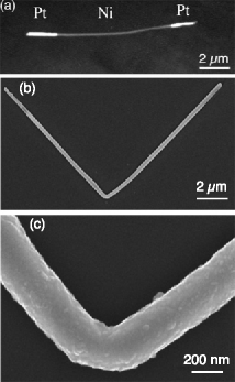
Metallic nanowires were grown via electrochemical deposition into the pores of nanoporous alumina templates.Possin70 ; Madsen85 ; Whitney93 ; Tanase01 The templates used were thick with a nominal pore diameter of 100 nm (Anodisk, Whatman, Inc.), with a 500 nm thick sputtered copper film serving as a working electrode. Platinum was deposited from a solution of 7.3 g/L and 58.3 g/L , buffered to pH 8.3 at a potential of -0.6 V relative to a Ag/AgCl reference electrode. Nickel was deposited from a solution of 20 g/L , 515 g/L , and 20 g/L , buffered to pH 3.4 at a potential of -1.0 V relative to a Ag/AgCl reference. Due to branching effects inside the pores, the actual diameters of the pores and hence of the nanowires, are significantly larger than the nominal diameter. Scanning electron microscopy (SEM) measurements on the nanowires showed diameters of nm. The nanowires were grown to lengths ranging from 20 to 40 microns. The majority of the wire length was nickel, with 2 of platinum at each end of the wire (see Fig 1(a)). These Pt endcaps provide a clean low-resistance electrical interface between the nickel segment and the contacts.Tanase02
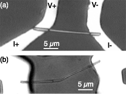
After fabrication, the alumina template was dissolved in a C KOH bath and the wires were resuspended in isopropanol. This suspension was then centrifuged for several minutes, inducing sharp bends at a range of angles into the nanowires. A SEM image of a nanowire with a bend is shown in Fig. 1(b), with a detail of the bend region shown in Fig. 1(c). This bending typically occurred near the center of the wire length. After bending, the wires were spun out onto a glass substrate, and an optical microscope equipped for projection photolithographyPalmer73 was used to pattern evaporated Cr/Au electrical contacts on top of the platinum endcaps of the nanowires. Nanowires were selected based on the angle and sharpness of the bend, and the straightness of the two segments. The contacts were patterned in a pseudo 4-probe geometry, as shown in Fig. 2.
Current-voltage (IV) measurements were performed on a series of straight PtNiPt nanowires of various lengths to determine the resistivity of the segments and the contact resistance. The IV curves were linear up to current densities of (I=0.5 mA), with Joule heating acting to increase the resistance at higher currents, up to a maximum breakdown current density of .Tanase02 The platinum segments showed a room-temperature resistivity of and the nickel had .TanaseUnpub Contact resistances between the electrodes and the nanowires were typically . The measured resistances decreased monotonically as the wires were cooled to 5 K, indicating that the contacts were metallic in nature and all interfaces were clean. Similar measurements on pure Ni nanowires showed insulator-like thermal behavior, which suggests the presence of surface oxide on the Ni and indicates the importance of the Pt segments for the success of these measurements.
The magnetotransport measurements on PtNiPt nanowires were made with a 100 Hz AC current source and a lockin amplifier. The measurements were made at room temperature, using an electromagnet equipped with a computer-controlled motorized rotating sample stage. A 2-axis Hall effect sensor (Sentron AG) was used to implement a closed feedback loop on the rotation system, giving an angular positional accuracy varying from at 4 kOe to at 500 Oe. Magnetoresistance hysteresis loops were obtained by ramping the field at rates ranging from 2 to 50 Oe/s and continuously measuring the resistance. The system also allowed for measurement of resistance at constant field while continuously changing orientation. In this mode, the stage was rotated at 0.5 deg/s. The feedback loop allowed for accurate comparisons between and measurements. In all cases, the field was in the plane of the substrate, with the rotation axis perpendicular to this plane.
III Straight nanowires
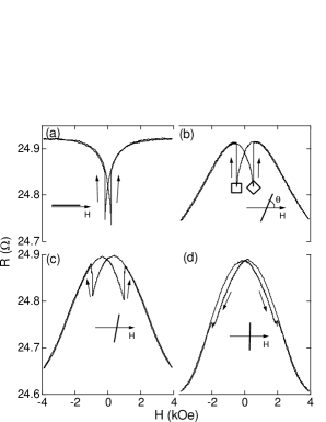
The magnetoresistance of a 20 m long straight nanowire is shown in Figs. 3(a)-(d) for four different orientations to the field. As has been seen in previous, in-template, measurements on similar wires, Wegrowe99 ; Jaccard00 there are two main features in the magnetoresistance. First, there is an overall non-hysteretic contribution due to the anisotropic magnetoresistance (AMR) effect in nickel.McGuire75 Our straight wires have a room temperature AMR of when the wire is perpendicular to the applied field. The decrease in the low-field resistance when the wire is parallel to the field (Fig. 3(a)) indicates that there is some demagnetization at low fields. This is discussed in more detail below. In addition to the non-hysteretic magnetoresistance, there is an abrupt increase in the resistance at a well defined magnetic field, known as the switching field .Wernsdorfer96 This hysteretic effect is due to the rapid reversal of the nanowire’s magnetization.Wegrowe99 When the nanowire is nearly perpendicular to the field, we frequently observe a splitting of the transition into two or more unequal steps. This can be seen in Figs. 3(c), (d) and 6(e). We believe that the presence of the smaller transitions is due to slight bends in the nanowire, and a consequent shift in the switching field. When such split transitions are observed, we define the overall switching field as the location of the largest step in the resistance.
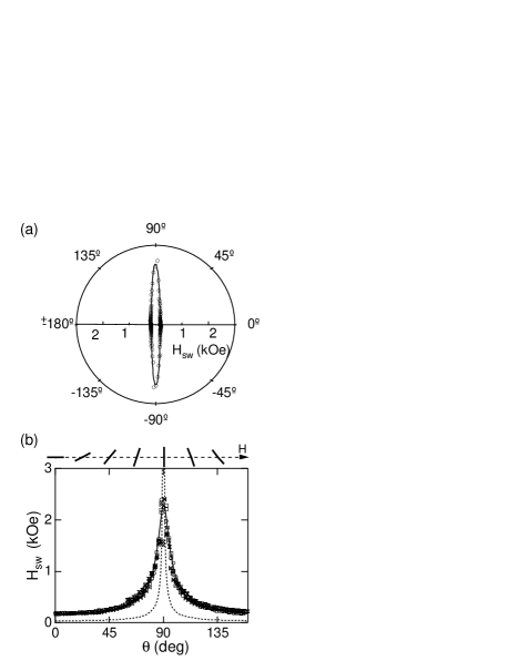
As can be seen from Fig. 3, the value of depends on the angle between the wire and the field. This is more evident in Fig. 4(a), which shows the angular dependence of the switching field. This figure can be viewed as a phase diagram for one particular nanowire. When a given location lies outside the elliptical region defined by the set of switching fields, the nanowire is in the reversible state, and the magnetization is single-valued, depending only on the values of and , and not on the wire’s prior history. On the other hand, when lies inside the set of switching points, the wire is in a hysteretic state, where the magnetization is multiply valued, and depends on the path followed. Fig. 4(b) shows the same switching field data as Fig. 4(a), plotted on a linear scale (showing ). In this panel, the reversible region lies above the plotted points, and the hysteretic region below. These measurements were repeated on a series of 350 nm diameter nanowires, with lengths ranging from 12 to 20 m. As can be seen from Fig. 4(b), is independent of wire length in this range.
Additional measurements were performed where the field was kept fixed and the wire was continuously rotated through two complete revolutions, one counterclockwise ( increasing) followed by one clockwise ( decreasing). Three such measurements on a straight nanowire are shown in Figs. 5(a)–5(c). The curvature seen in is due to the magnetization of the wire rotating towards the direction of the field and hence away from the axis of the wire. The resistance follows , as would be expected from the AMR of a cylinder. The rotation sweeps also show sharp switching events that are very similar to those seen in the field sweeps discussed previously. These measurements also show hysteretic behavior. This can be understood by tracking the direction of the magnetization in the wire as it is rotated. Initially (), the wire is parallel to the field, along with the magnetization. As the wire is rotated, the strong shape anisotropy tends to make the direction of M rotate away from the field, tracking the wire axis. This continues as the wire rotates past perpendicular, with the magnetization becoming increasingly anti-aligned to the field. At a certain orientation (), this anti-aligned magnetization becomes energetically unstable, and the magnetization undergoes a rapid reversal in direction to become aligned with the field. This produces the sharp increases in the resistance seen in Fig. 5. When the direction of rotation is reversed, the same behavior is observed. However, since the reversal occurs after the nanowire rotates past perpendicular to the field, the magnetization, and hence the resistance, is hysteretic.
As with the measurements discussed above, the data can be divided into two regions, where the resistance is either reversible or hysteretic. The boundary between these two regions can be determined by plotting as a function of the applied field, as shown in Fig. 5(d). The smooth curve in Fig. 5(d) is the fit to the data (discussed below) shown in Fig. 4. and closely overlap, indicating that the location of the phase boundary does not change depending on which variable is being swept. This is further illustrated by comparing the data shown in Fig. 3(b) (R vs. H at ) with the data in Fig. 5(b) (R vs. at H=500 Oe). The open diamond on both of these panels marks a switching event at , H=500 Oe. Similarly, the open square marks a switching transition at , H=-500 Oe, or equivalently, , H=500 Oe.
To determine the reversal mode of these nanowires, we examine the shape of . As shown in Fig. 4, is peaked near (wire perpendicular to field) and has a minimum at (wire parallel to field). This angular dependence allows us to rule out Stoner-Wohlfarth, or coherent rotation, as the reversal mechanism, as that reversal mode has peaks in the switching field when the wire is both perpendicular and parallel to the field.Stoner48 This suggests that the reversal mechanism for the wire is incoherent rotation, or curling,Brown57 consistent with expectations based on the diameter of the nanowire,Aharoni00 as well as previous magnetic force microscopy studies on Ni nanowires of comparable size.Lederman95
For an ellipsoid reversing its magnetization through the curling mode, it has been predictedAharoni97 that the switching field follows
| (1) |
where is the saturation magnetization, and are the demagnetization factors along the major and minor axes of the ellipsoid, and . Here, is the minor radius of the ellipsoid, is the exchange length of the ferromagnet, and is a geometrical factor dependent on the aspect ratio of the prolate spheroid. From the nanowire’s length of and radius , the demagnetization factors are and .Morrish83 The saturation magnetization is assumed to be the bulk nickel value, . The exchange length for nickel is known to be approximately 20 nm,Brown57 ; Lederman95 and for an extended cylinder is 1.079.Aharoni97 The predicted curve, shown as the dashed line in Fig. 4, clearly does not match the observed switching fields for our wires. However, it has been suggested that the magnetization reversal proceeds via an initial nucleation in a small volume of the wire, and subsequent propagation throughout the entire wire.Wegrowe99 This assumption does fit the observed data (solid line in Figs. 4(a), 4(b), and 5(d)), with free parameters and , corresponding to a nucleating region of aspect ratio 1.3:1 and radius . This nucleation region occupies 0.5% of the total wire volume. The size of this nucleation region is comparable to previously determined values in nanowires of smaller diameter.Jaccard00 As noted above, for several of our straight nanowires have the same shape; this indicates that the size and shape of the initial nucleation volume does not vary signficantly between wires with different lengths.
To examine the energetics of the nanowire reversal process, we have developed a phenomenological model to describe the behavior of the magnetization. We begin by assuming that, except at the switching field, the direction of the magnetization is described by Stoner-Wolhfarth coherent rotation,
| (2) |
where is the angle between the applied field and the wire axis, and is the angle between the magnetization vector and the wire axis.Aharoni00 Because the nanowire is initially being modeled as single domain, the demagnetization factors used in this calculation are derived from the geometry of the entire wire (, ), and not from the nucleation volume determined from the curling mode fit. The resistance is then related to the magnetization by . At , the shape anisotropy forces the magnetization to lie along the axis of the wire (), indicating that the resistance should be maximized at zero field. However, the observed resistance data shown in Fig. 3 have maxima that are at non-zero field. This implies that there is a demagnetization effect at low field that reduces the overall magnitude of M. A possible mechanism for this effect is that the magnetization is rotating towards the crystalline easy axis of the wire. Since these nanowires are polycrystalline, there will be a distribution of these directions, resulting in a decrease in the net magnetization.
To model this behavior in the data, we assume that the S-W theory provides an accurate description of the direction of the magnetization, but that there is a spatially-uniform demagnetizing effect that reduces the magnitude. In the absence of direct data on the magnitude of the magnetization, we assume a simple analytic form,
| (3) |
where the sign of depends on which branch of the hysteresis is being followed. The expression for the magnetoresistance is then modified to
| (4) |
and this expression is fit to the observed data using , , , and as free parameters. We use the switching field calculated from the small nucleation volume curling mode fit described above, and not by the Stoner-Wohlfarth coherent rotation mode. The best-fit magnetization curves and calculated resistances for two orientations are shown in Fig. 6. The exact functional form of the demagnetization curve Eq. (3) does not have a major effect on the quality of the model. A Langevin function () works as well as the that was used in Eq. (3).
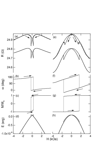
As can be seen from the figure, this approach produces calculated magnetoresistance curves that closely match the observed data, and hence this modeling procedure provides a good description of the magnetic response of the wire. The magnetization information obtained from the fit can then be used to calculate the magnetostatic energy of the nanowire. For an extended ellipsoid, the energy is given by
| (5) |
where is the volume of the wire and is the component of the magnetization along the wire axis.Aharoni00 The field dependence of this energy is shown for two orientations of a straight wire in Fig. 6(c),(f). The magnetic reversal corresponds to a transition from a high-energy to a low-energy state, with a typical change in energy of erg, compared to a total magnetostatic energy on the order of erg.
IV Bent nanowires
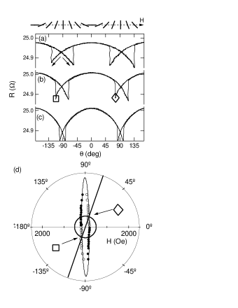
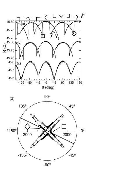
The magnetoresistance behavior of bent wires is signficantly different from that of the straight wires, as illustrated in Fig. 7 for a 40 wire with a bend, and in Fig. 8 for a wire of the same length with a bend. The non-hysteretic AMR component of the resistance is never flat, as it is for straight wires when . In addition, most orientations show jumps in the resistance at two distinct fields, indicating the presence of two magnetization reversals. The switching fields vs. wire orientation for the and bent wires are shown in Fig. 9 and Fig. 10. For each wire, there are two peaks in , each occuring when one of the segments is perpendicular to the field. As indicated in panel (b) of each figure, the separation between the peaks is equal to the bend angle for each wire. From this, the basic similarity of the individual peaks, and the comparable height of the resistance steps to that observed in the straight wires, we infer that the two resistance steps observed in correspond to magnetization reversals in the individual segments, with the higher field feature coming from the segment that is oriented at the larger angle with respect to H. It should be noted, however, that not all orientations show two switching transitions. For each bent wire, there is a range of orientations (marked by open triangles on Fig. 9 and Fig. 10) where only a single transition is observed. The implications of this are discussed below.

As in the case of the straight nanowires, Fig. 9 and Fig. 10 represent phase diagrams for the bent nanowires. In this case, the shape of the phase boundaries is more complicated, because of the presence of two segments at differing orientations. The overall nature of the diagram, however, is the same, with a reversible region that lies outside the curve, and a hysteretic region inside the curve.
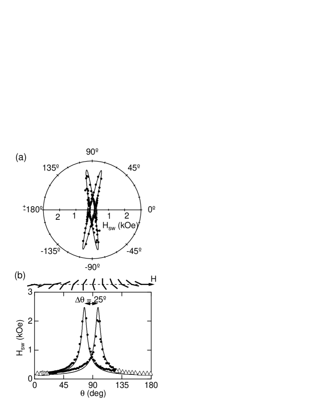
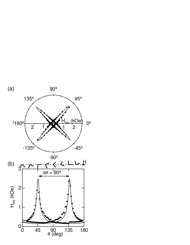
Figure 11(a)–(c) shows measurements at a range of fields for a nanowire with a bend. As in the straight wires, switching transitions in the bent wires are observed at the same set of locations in both the and the measurements. This is illustrated in Fig. 11(d), where the smooth curves shown in Fig. 10 are superimposed over the measured from the measurements. The two data sets match well. This is seen in more detail by comparing a field sweep at (Fig. 8(b)) to an angle sweep at H=450 Oe (Fig. 11(b)). The trajectories in that these two data sets describe are marked in Fig. 11(d) by a straight line and circle, respectively. The switching events on these two scans occur in the same location, indicated on the plots by an open diamond and square.
As a starting point, the angular dependence of the switching fields in the bent nanowires can be modeled by assuming that the two segments of the wire switch independently. If this assumption is accurate, then the curling-mode fit discussed above for the straight wire should also apply to bent wires when suitably offset in angle to account for the different relative orientation of the two segments to the field. As seen in Fig. 9(b) and Fig. 10(b), these curves qualitatively match the observed behavior of the bent wires, indicating that independent-segment curling is a reasonable first approximation for describing the switching behavior.Tanase03 There are, however, systematic deviations between the data and the model, indicating that the first-order approximation of the bent wire as two independent straight segments is incomplete. To understand these deviations, it is necessary to examine interaction effects between the segments.
IV.1 Effects of domain configuration on
Before discussing the effects of intersegment interactions, it is first necessary to examine how the domain configuration in a bent nanowire varies with angular orientation. This can be examined using magnetic force microscopy (MFM) on bent nanowires. MFM images were acquired with a Nanoscope III Multimode AFM/MFM (Digital Instruments). An example is shown in Fig. 12. Fig. 12(a) shows an atomic force microscope topographic image. In Fig. 12(b), the nanowire was initially magnetized in a strong vertical field, and subsequently imaged by MFM at zero field. The MFM picture shows a positive pole at one end of the wire and a negative pole at the other end, with no pole at the bend. The absence of a pole in the body of the wire indicates that the magnetization is continuous, with no domain wall present. In Fig. 12(c), the same nanowire was remagnetized in a strong horizontal field and a zero-field image was again obtained. Here, the poles at the wire ends are both positive, and there is a strong negative pole at the bend. The pole at the bend is a signature of a the presence of a domain wall at the center of the wire. This central pole was measured to have a width of , significantly larger than the typical 100 nm domain wall width in nickel.Gregg96 We believe that this increase in the size of the domain wall is associated with the extended curvature at the bend region.
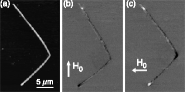
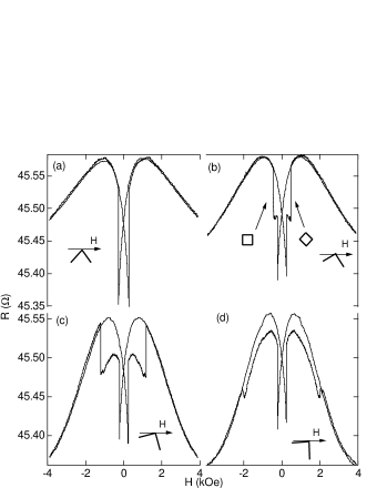
The orientation dependence of the domain structure can be understood by considering the schematic of the magnetization structure shown in Fig. 13. At an initial large positive field (a,e), the applied field dominates over the shape anisotropy and the segments’ magnetizations rotate off the segment axis and towards the applied field. When the field is reduced to zero, the magnetizations relax back towards the segment axes (b,f). The MFM images were taken at this point, with Fig. 12(b) corresponding to the schematic magnetization in Fig. 13(b), and similarly for Fig. 12(c) and Fig. 13(f). At some negative field, the segment that is nearly parallel to the field undergoes a switching transition, reversing its magnetization direction (c,g). At this point, the wire configuration shown in (c) has a domain wall at the bend; we therefore term this the “wall” orientation. On the other hand, the magnetization in (g) does not have a domain wall, but instead has a continuous rotation of the magnetization direction between the two segments. This orientation is thus designated the “no-wall” state. At larger negative field, the magnetization of the near-perpendicular segment reverses, and the magnetization for both segments again rotates off-axis (d,h) as in (a,e).

The most visible deviation from the independent segment picture occurs near and , where the two segments are at similar angles to the field. If the two segments of the bent wire were not coupled, they would switch simultaneously if and only if their angles to the field were the same. For all other orientations, the segments would have different switching fields. In the actual bent wires, however, a single simultaneous transition is seen even when the angles are not the same. This is shown in Fig. 14, which compares the MR of a straight wire at and to the field to the resistance of a bent wire whose segments are at comparable orientations. The straight wire switches at different fields in the two orientations, whereas the bent wire’s response is dominated by a single large jump in the resistance, indicating that both segments switch simultaneously. This “locking” of the switching of the segments occurs over a wide range of orientations, indicated by the solid triangles in Fig. 9 and Fig. 10.
The reversal locking occurs in regions where the wire orientation is similar to the left column in Fig 13. This region is found at and in Fig. 9 for the bent wire and and in Fig. 10 for the wire. The locking occurs because the energy cost of nucleating a domain wall to enter the intermediate state (c) makes it energetically favorable to suppress the separate transitions and reverse the entire wire simultaneously. The locked transitions are shown in Figs. 9 and 10 as open triangles. An estimate for the energy cost of domain nucleation can be determined by considering the shift in the switching fields and the additional magnetostatic energy associated with that shift. For the orientations shown in Fig. 14, this shift is approximately 35 Oe. This corresponds to an increase of energy of erg, approximately 1% of the total energy of the nanowire.
When the two segments of a bent wire are at sufficiently different angles to the field, the wire reverses its magnetization in two separate steps. There is still an energy cost for switching into the anti-aligned intermediate state, which appears as an increase in the switching field of the segment closer to parallel to the field. This can be seen most clearly in Fig. 10 for and , where the measured switching fields (circles) are larger than what was expected based on the straight wire results (smooth curve). At higher field, the reversal of the segment closer to perpendicular to the field places the wire back into an aligned magnetization state. This is an energetically favorable transition, and in this regime, the straight wire data matches the behavior of the bent wire.
The opposite behavior is observed when the wire is in an orientation similar to the right column of Fig. 13. For the bent wire, this occurs for in Fig. 10. In this orientation, the low-field reversal (of the segment more nearly parallel to the field) places the wire in a single domain state. Since there is no additional energy barrier due to the creation of a domain wall, the behavior of the bent-wire switching field is accurately predicted by the straight wires. On the other hand, the subsequent reversal of the more nearly perpendicular segment places the wire in an anti-aligned magnetization state. The cost of nucleating a wall results here in an increase in the switching field in this regime. This is seen in Fig. 10 as a shoulder in the peaks for compared to the prediction from the straight wire data.
It should be noted that these shifts in the switching fields for the bent nanowires cannot be ascribed to differences in the lengths of the two segments. The switching field data for the series of straight nanowires shown in Fig. 4(b) indicate that there is very little variation in in the range of lengths studied. This range of lengths encloses the lengths of the segments of the bent nanowires studied. This implies that the changes in in the bent wires are not simply due to differences in the segment lengths.
IV.2 Domain wall resistance
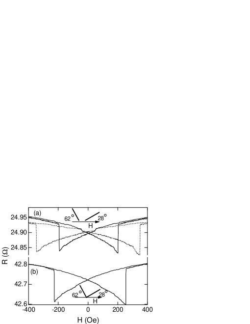
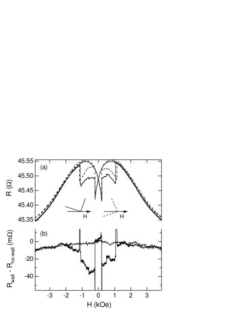
In addition to shifting the switching fields, the domain configuration effects can be observed directly in the magnetoresistance data. This can be seen by comparing the MR curves for a bent wire in two orientations, corresponding to those in Fig. 13, with the same angles between the segments and the applied field. The magnetoresistance for one such pair of orientations is shown in Fig. 15(a). The solid curve, corresponding to the orientation in the left column of Fig. 13 (“wall” orientation), has a domain wall in the region where only one segment has reversed. The dashed curve, corresponding to the other (“no-wall”) orientation, does not have a domain wall in this region. Since the angles between the segments and the field are the same, we would expect the magnetoresistances to be the same, with some differences in the switching fields due to the energetic effects discussed above. Instead, there is a significant difference in the intermediate region, where only one of the segments has reversed. This is shown in more detail in Fig. 15(b), which plots the differences between the two curves. The solid curve (“wall” orientation) has a lower resistance in the intermediate region, suggesting that there is a decrease in the resistance associated with the presence of a domain wall. This decrease was seen in measurements on multiple bent wires, with magnitudes in the range of , corresponding to a fractional change in the resistance of . We note that the bend angle needs to be near to allow a comparison of this sort to be made. This result is somewhat analogous to what was observed by Taniyama et. al in lithographically-defined zigzag structures at lower temperatures.Taniyama99
There are multiple theoretical models that include the possibility of domain walls with negative contributions to the resistance. Tatara and FukuyamaTatara97 have proposed a mechanism based on the suppression of weak localization. Using the dimensions of our nanowire in their theory gives a predicted wall resistance of , comparable to the measured value. However, it is unlikely that weak localization effects play a significant role at room temperature, indicating that an alternate explanation is required. van Gorkom et al.vanGorkom99 have proposed a semi-classical mechanism based around differing scattering relaxation times for the majority and minority spin channels. Depending on the ratio of these times, the wall resistance can be either negative or positive, with values in the range . This range encompasses the observed values in our nanowires, but in the absence of detailed information on the nature and density of the impurities in the nickel, we are unable to make a more precise comparison between the theory and our data.
Another effect that can provide negative wall resistance is the AMR contribution from the spins inside the wall itself.Hong98 ; Taniyama99 Based on the MFM results shown in Fig. 12, the domain wall width in the bent wires is on the order of . Given the straight wire satuartion magnetoresistance of , this corresponds to a decrease in the resistance of , approximately one third of the decrease actually observed. Thus, while it appears that AMR plays a significant role in the resistance shift, it seems likely that there are other mechanisms contributing to this effect and that further investigation is necessary to determine its cause.
V Conclusions
In summary, we examined the magnetotransport properties of straight and bent ferromagnetic nanowires. It was determined that the switching behavior of the straight nanowires is consistent with the curling-mode reversal of a small volume, followed by propagation throughout the wire bulk. The bent wires showed qualitatively similar behavior, with modifications from the intersegment interactions. For both the straight and bent nanowires, the location of the switching events in were found to be independent of which variable was being swept. The magnetic properties of the bent wires were dependent on the domain configuration at the bend; the energetic cost of nucleating a domain wall acts to increasd the observed switching field compared to a straight wire at equivalent orientations. There is also a change in the resistance associated with the domain configuration; the resistance is lower when a domain wall is present. Further investigation is needed to determine the mechanism of this reduction, including examination of wires of differing diameters and possible studies of the dynamics of the reversal. Thus it appears that magnetic nanowires are a fruitful system for future studies of reversal dynamics and the effects of domain walls in ferromagnets.
VI Acknowledgments
We thank M. Stiles and P. Searson for illuminating discussions. This work was supported by NSF Grant No. DMR–0080031.
References
- (1) A. Fert and L. Piraux, J. Magn. Magn. Mater. 200, 338 (1999).
- (2) W. Wernsdorfer, B. Doudin, D. Mailly, K. Hasselbach, A. Benoit, J. Meier, J.-Ph. Ansermet, and B. Barbara, Phys. Rev. Lett. 77, 1873 (1996).
- (3) Y. Jaccard, Ph. Guittienne, D. Kelly, J.-E. Wegrowe, J.-Ph. Ansermet, Phys. Rev. B. 62, 1141, (2000).
- (4) A. Radulescu, U. Ebels, Y. Henry, K. Ounadjela, J.-L. Duvail, and L. Piraux, IEEE Trans. Magn. 36, 3062 (2000); U. Ebels, A. Radulescu, Y. Henry, L. Piraux, and K. Ounadjela, Phys. Rev. Lett. 84, 983 (2000).
- (5) M. Lederman, R. O’Barr, and S. Schulz, IEEE Trans. Magn. 31, 3793 (1995); R. O’Barr and S. Schulz, J. Appl. Phys. 81, 5458 (1997).
- (6) J-E. Wegrowe, D. Kelly, A. Franck, S. E. Gilbert, and J.-Ph. Ansermet, Phys. Rev. Lett. 82, 3681 (1999).
- (7) M. Tanase, L. A. Bauer, A. Hultgren, D. M. Silevitch, L. Sun, D. H. Reich, P. C. Searson, and G. J. Meyer, NanoLett. 1, 155 (2001).
- (8) M. Tanase, D. M. Silevitch, A. Hultgren, L. A. Bauer, P. C. Searson, G. J. Meyer, and D. H. Reich, J. Appl. Phys. 91, 8549 (2002).
- (9) G.R. Taylor, A. Isin, and R.V. Coleman, Phys. Rev. 165, 621 (1968).
- (10) J.F. Gregg, W. Allen, K. Ounadjela, M. Viret, M. Hehn, S.M. Thompson, and J.M.D. Coey, Phys. Rev. Lett. 77, 1580 (1996).
- (11) U. Rudiger, J. Yu, L. Thomas, S.S.P. Parkin, and A.D. Kent, Phys. Rev. B. 59 11914 (1999).
- (12) J. L. Prieto, M. G. Blamire, and J. E. Evetts, Phys. Rev. Lett. 90, 027201 (2003).
- (13) K. Hong and N. Giordano, J. Magn. Magn. Mater. 151, 396 (1995); K. Hong and N. Giordano, J. Phys. Condensed Matter 10, L401 (1998).
- (14) T. Taniyama, I. Nakatani, T. Namikawa, and Y. Yamazaki, Phys. Rev. Lett. 82, 2780 (1999); T. Taniyama, I. Nakatani, T. Yakabe, and Y. Yamazaki, Appl. Phys. Lett. 76, 613 (2000).
- (15) U. Ruediger, J. Yu, S. Zhang, A.D. Kent, and S.S.P. Parkin, Phys. Rev. Lett. 80, 5639 (1998).
- (16) Y.B. Xu, C.A.F.Vaz, A. Hirohata, H.T. Leung, C.C. Yao, J.A.C. Bland, E. Cambril, F. Rousseaux, and H. Launois, Phys. Rev. B. 61 R14901 (2000).
- (17) P. Levy and S. Zhang, Phys. Rev. Lett. 79, 5110 (1997).
- (18) E. Simanek, Phys. Rev. B. 63, 224412 (2001).
- (19) G. Tatara and H. Fukuyama, Phys. Rev. Lett. 78, 3773 (1997).
- (20) R.P. van Gorkom, A. Brataas, and G.E.W. Bauer, Phys. Rev. Lett. 83, 4401 (1999).
- (21) G.E.Possin, Rev. Sci. Instrum. 41, 772 (1970).
- (22) J.T. Masden and N. Giordano, Phys. Rev. B, 31, 6395 (1985).
- (23) T.M. Whitney, J.S. Jiang, P.C. Searson, and C.L. Chien, Science 261, 1316 (1993).
- (24) D. W. Palmer and S. K. Decker, Rev. Sci. Instrum. 44, 1621 (1973).
- (25) M. Tanase et al., unpublished.
- (26) T. R. McGuire and R. I. Potter, IEEE Trans. Magn. 11, 1018 (1975).
- (27) E. C. Stoner and E. P. Wohlfarth, Phil. Trans. Roy. Soc. 240, 599 (1948).
- (28) W. F. Brown, Phys. Rev. 105, 1479 (1957).
- (29) A. Aharoni, Introduction to the Theory of Ferromagnetism, Oxford University Press, New York (2000).
- (30) A. Aharoni, J. Appl. Phys. 82, 1281 (1997).
- (31) A. H. Morrish, The Physical Properties of Magnetism, Robert Krieger Publishing Company, Malabar Florida, (1983). We use the convention that .
- (32) M. Tanase, D. M. Silevitch, C.L. Chien, and D. H. Reich, J. Appl. Phys. 93, 7616 (2003).