Normal-state conductivity in underdoped La2-xSrxCuO4 thin films: Search for nonlinear effects related to collective stripe motion
Abstract
We report a detailed study of the electric-field dependence of the normal-state conductivity in La2-xSrxCuO4 thin films for two concentrations of doped holes, and 0.06, where formation of diagonal and vertical charged stripes was recently suggested. In order to elucidate whether high electric fields are capable of depinning the charged stripes and inducing their collective motion, we have measured current-voltage characteristics for various orientations of the electric field with respect to the crystallographic axes. However, even for the highest possible fields ( V/cm for and V/cm for ) we observed no non-linear-conductivity features except for those related to the conventional Joule heating of the films. Our analysis indicates that Joule heating, rather than collective electron motion, may also be responsible for the non-linear conductivity observed in some other 2D transition-metal oxides as well. We discuss that a possible reason why moderate electric fields fail to induce a collective stripe motion in layered oxides is that fairly flexible and compressible charged stripes can adjust themselves to the crystal lattice and individual impurities, which makes their pinning much stronger than in the case of conventional rigid charge-density waves.
pacs:
74.25.Fy, 74.72.Dn, 71.45.Lr, 72.20.HtI Introduction
The parent compounds of high- cuprates are known to be correlated Mott insulators that become metallic and superconducting (SC) upon doping with charge carriers; the mechanism of this evolution, however, still remains a mystery. One of the possible pictures is that the doped holes segregate, instead of being homogeneously distributed, and establish an array of microscopic conducting channels (charged stripes) embedded in the insulating matrix.stripe_rev ; NdSr ; diag_ver ; mobility ; anis In fact, these conducting channels reduce the penalty for disrupting the correlated insulating state, and allow even a few holes to move through a Mott insulator. Owing to the long-range Coulomb interaction, the hole-rich channels tend to order into a fairly periodic pattern, reminiscent of the charge-density wave (CDW) in quasi-1D conductors.CDW_rev Periodic charge-density modulations have indeed been found in some of the cuprate compounds, stripe_rev ; NdSr ; 1eighth giving support to the stripe picture.
Despite the resemblance, the charged stripes differ from conventional CDW both in properties and in the mechanism driving their formation: A conventional CDW is governed by the Fermi-surface instability of a metal and results in opening of a gap exactly at the Fermi level,CDW_rev while charged stripes stem from the tendency of doped holes to avoid localization, and do not require such gap formation.stripe_rev The absence of a gap at the Fermi level allows the stripes to be conducting, and also makes them compressible – the hole filling of stripes as well as the distance between them should be readily variable. Consequently, the conducting stripes may well be flexible and fluctuating in contrast to rather rigid CDW.
Apparently, those strong fluctuations make the stripes in cuprates quite elusive, causing many experiments aimed at observing the stripes to fail. Although one can easily find evidence for microscopic charge inhomogeneity, no static stripe ordering is observed unless a strong collective pinning (commensurability effects at filling, structural distortions in La2-x-yNdySrxCuO4, etc.) fixes the position and orientation of the stripes in CuO2 planes, making them visible for diffraction techniques.stripe_rev ; NdSr ; 1eighth This naturally casts doubts on whether the stripes are inherent in cuprates and ultimately relevant for high- superconductivity, or the observed stripy superstructures are just a side effect caused by lattice instabilities. Even more challenging is to find out what are the new qualitative features that the charged stripes are bringing about.
Upon selecting experiments to clarify the role of stripes, one may consult how the existence of collective electron states has been substantiated in other systems, particularly when diffraction methods were incapable of giving a conclusive evidence. In the field of inorganic quasi-1D compounds, the key experiments that have led the CDW picture to triumph, and have ultimately convinced researchers that they are dealing with a truly collective state, were (i) observation of a sharp threshold electric field in conductivity, corresponding to the onset of coherent CDW sliding, and (ii) observation of a “narrow-band noise” induced by the motion of a washboard-like CDW over defects.CDW_thr The transport measurements were certainly indispensable for 2D electron systems (2DES) in heterostructures, where a conducting layer is buried deep in the crystal and diffraction methods can hardly be used. A variety of collective electron states including stripe, “bubble”, and Wigner-crystal phases expected 2DEG_the to be realized in 2DES were also documented by observations of threshold conduction and narrow-band noise.Wign ; 2DEG1 Another class of experiments is related to qualitatively new features introduced by the collective state to the single-particle transport. The most fascinating among those is the observation of a large resistivity anisotropy which spontaneously develops in seemingly isotropic 2DES at low temperatures, and whose orientation can be switched by a magnetic field. 2DEG2
In cuprates, the qualitative evidence for conducting stripes, collected thus far from transport measurements, is limited to a spontaneous (or field-induced) in-plane resistivity anisotropy that develops at low temperatures, anis in striking resemblance to 2DES. A suppression of the Hall resistivity in the static-stripe system La2-x-yNdySrxCuO4, initially considered as a clear evidence for 1D transport, Hall has been later understood as coming from a tricky cancellation of the hole and electron terms, which may or may not be related to the 1D hole motion; in fact, such Hall-resistivity suppression is a rare exception among cuprates. mobility ; Hall2 It might sound surprising, but such key features as narrow-band noise or threshold conductivity have never been seriously looked for in high- cuprates, though non-linear conduction has been observed in ladder cuprates. ladder ; ladder2 This is partly because of a common wisdom which tells us that the CDW (or stripe) sliding is hardly possible in 2D/3D systems because of too strong pinning. However, this understanding has been challenged recently by a number of papers reporting spectacular non-linear conduction in layered nickel and manganese oxides, Nature ; Science ; LaSrNiO ; film ; film_perp which has been attributed to the collective charge motion and the collapse of the charge-ordered state. If this interpretation is actually correct, one may look for similar stripe-sliding effects in cuprates cuprates which, if found, would finally clarify the electronic state underlying the high- superconductivity.
In this study, we search for non-linear conductivity features in the most promising system La2-xSrxCuO4 (LSCO), where static and dynamic stripes of different topology have been observed by neutron scattering.stripe_rev ; NdSr ; diag_ver The compositions and are chosen as representing the “diagonal” and “vertical” stripe statesdiag_ver (Fig. 1). In order to minimize the Joule heating, we prepare LSCO thin films patterned into narrow bridges, which allows us to perform current-voltage-characteristics measurements up to electric fields of 100-1000 V/cm. The bridges are formed along several crystallographic directions, making possible the field application along or transverse to the expected stripe direction. However, up to the highest electric fields we observe no non-linear conductivity features other than those related to the Joule heating. This indicates that the electric-field energy integrated over the correlated stripe volume (if the stripe picture is actually appropriate for cuprates) is still too weak to overcome pinning and to drive the stripe sliding. Consequently, the correlated volume for the stripe ordering in cuprates appear to be much smaller and the stripe pinning to be much stronger than in conventional CDW systems,CDW_theo and moderate electric fields may never be able to induce the stripe sliding. Furthermore, a simple analysis of Joule heating shows that electric fields of the order of 100-1000 V/cm represent a characteristic threshold for many “insulating” transition-metal oxides. For fields above this threshold, the samples must show non-linear conductivity and switching phenomena which, however, are related neither to collective charge motion, nor to other electronic peculiarities, but are caused simply by overheating. This calls for more caution in interpreting numerous observations of the non-linear conduction in transition-metal oxides.
II Experimental details
A difficult problem one inevitably faces upon measuring the high-electric-field characteristics is the Joule overheating of samples. Often used simultaneous current and voltage limitations Nature ; Science ; LaSrNiO ; film ; film_perp merely result in stabilizing an inhomogeneous state, e.g., composed of conducting filaments,Bonch ; hot_spot which hides the intrinsic behavior. Another approach is to employ short-pulse technique; however, to reduce overheating to a reasonable level, the pulses should be as short as 1 s or less in most cases.mesa_heat ; hot_spot For CDW systems possessing huge dielectric constants and strong frequency dependence of the conductivity, CDW_rev such short-pulse measurements would give data that have nothing to do with the dc conduction. Apparently, the only effective approach is to reduce the size of samples in order to decrease the produced heat and to ease the heat removal. This miniaturization is naturally limited by the characteristic correlation length of the ordered state under investigation, when the surface pinning and size effects become important.CDW_size For high-electric-field measurements, therefore, we chose thin-film samples, and employed a conventional dc four-probe method.
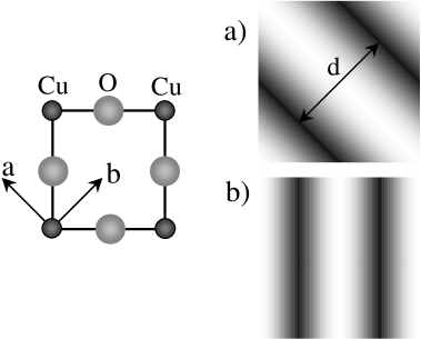
Epitaxial La2-xSrxCuO4+δ films with and 0.06 were prepared by a conventional pulsed-laser deposition technique. During the growth, the temperature of the substrate was set at 800 C, and the oxygen pressure was kept around 4 Pa. An important point was a proper choice of substrates, in order to minimize any unwanted film distortion induced by the lattice mismatch. Since LSCO with the composition was orthorhombic and was expected to possess “diagonal” stripes running along one of the orthorhombic Cu-Cu directions (Fig. 1), we selected orthorhombic YAlO3 (YAP) substrates for growing LSCO films. In doing so, we intended to obtain films with perfectly aligned crystallographic axes, and thus possessing a unidirectional stripe structure. We indeed succeeded in growing untwinned La1.99Sr0.01CuO4 films on the (001) surface of YAP, where the in-plane orientation LSCO [100] was parallel to YAP [100], according to the x-ray diffraction. LSCO films, which were expected to have “vertical” stripes, were prepared on the (100) surface of SrTiO3 (STO) and (001) surface of LaSrAlO4 (LSAO) substrates. Both STO and LSAO have a slight lattice mismatch with LSCO, yet this mismatch is of different signs; thus, the LSCO films deposited on these substrates are subject to an expansive and compressive in-plane strain, respectively.strain Since the epitaxial strain can easily affect the stripe pinning, as it does with the superconducting transition temperature, we use films both on STO and LSAO for a comparative study of the current-voltage characteristics.
The thickness of prepared La2-xSrxCuO4+δ films was determined to be Å and 2400 Å for films, and Å for films (a piece of film was dissolved in acid and the amount of material was measured by the inductively-coupled plasma spectrometry). Each film was patterned into narrow, m, bridges aligned along the Cu-Cu or Cu-O-Cu directions, using photolithography. Electric contacts were made by gold paint with subsequent annealing in pure helium (for films) and in air (for films), following the heat treatment procedure developed for bulk crystals, anneal which is required to establish the oxygen stoichiometry .
The current-voltage characteristics were determined by applying a small low-frequency ac modulation voltage to the sample while a dc bias voltage was slowly swept, and measuring the differential conductance . Upon measurements, the substrate with sample was attached to a copper block, whose temperature was stabilized with an accuracy better than 0.01 K. The angular dependence of the magnetoresistance (MR) was measured by rotating the sample at the fixed temperature and magnetic field.
III Results and discussion
III.1 Resistivity and magnetoresistance
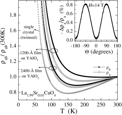
It is well known that crystal defects and strains, including those induced by a mismatch with the substrate, grain boundaries or surface effects, can easily pin the CDW/stripe structure, preventing it from sliding.CDW_rev ; CDW_size It is important, therefore, to obtain thin-film samples with properties not much different from those of high-quality single crystals. In the case of light doping (), we have succeeded in preparing LSCO films on YAlO3 with the resistivity behavior quite similar to that of single crystals,mobility but the film thickness had to be kept above Å (Fig. 2). A resistivity upturn appears at somewhat higher temperatures in thinner films, indicating easier localization of holes and larger disorder.
According to the neutron-scattering data, compositions with possess unidirectional stripes running along the orthorhombic axis. diag_ver In order to compare characteristics along and transverse to the stripes, one needs a single-crystalline film with uniform orientation of the orthorhombic and axes. Previous studies suscept ; MR_LSCO of detwinned LSCO single crystals have revealed a strong in-plane anisotropy of the susceptibility and magnetoresistance: When a magnetic field is applied along the plane, only the component of the field affects the spin and stripe structure and causes magnetoresistance.MR_LSCO Our LSCO films actually demonstrate a clear angular dependence of the MR (inset of Fig. 2), indicating the crystallographic axes are perfectly aligned.
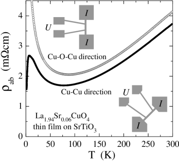
The composition is located just on the verge of the superconductivity, where the stripes are also reported to change their orientation from “diagonal”, that is being parallel to the orthorhombic axes, to the “vertical” one. Correspondingly, to check all possible geometries, we prepared bridges directed along the “diagonal”, Cu-Cu, and “vertical”, Cu-O-Cu, directions (insets of Fig. 3). The resistivity behavior of LSCO films deposited on SrTiO3 and LaSrAlO4 substrates (Figs. 3 and 4) demonstrates that they are of high quality: The resistivity values are close to those observed in the best single crystals,mobility K mcm, and the linear fitting of the high-temperature resistivity () gives , indicating negligible impurity scattering. The films however show some dispersion in properties. For example, in films on STO (Fig. 3), both resistivity and vary, indicating slightly different doping levels. In films on LSAO (Fig. 4), the doping seems to be the same for all films, as follows from the position of the SC transition (inset of Fig. 4), yet the resistivity does vary. Nevertheless, for this particular composition on the border of the superconductivity region (), one can hardly achieve better homogeneity: SC transitions depicted in the inset of Fig. 4 are already among the narrowest ever reported for single crystals or thin film.mobility
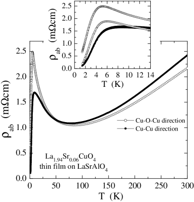
The low-temperature resistivity upturn in Figs. 2 - 4 reflects the process of collective – caused by the stripe pinning – or individual localization of holes. At low temperatures, neutron scattering also showed the dynamic stripe correlations to slow down and to evolve into a static order.diag_ver Apparently, it should be this region where one may expect high electric fields to overcome the pinning and to cause non-linear conductivity features.
III.2 Overheating effects
Before proceeding to the measurements, let us first consider the current-induced Joule heating, and estimate how high an electric field can be applied to a bridge without causing a significant increase of its temperature. For the geometry of narrow bridges, where both the produced heat and the heat removal scale with the bridge’s length, the overheating can be estimated rather easily, without complicated mathematics hot_spot required for bulk samples. Taking a typical thin (0.1 m) bridge with a width of 25-50 m, and assuming the substrate to be thermally anchored at a distance of mm, one can calculate the bridge overheating to be , where is a power being dissipated per unit length of the bridge and is the thermal conductivity of the substrate. We can therefore estimate the actual temperature for each bridge, , as a function of the applied electric field, using experimental resistivity data :
| (1) |
where is the bridge’s cross-section, and is an effective heat conductivity in the range to .
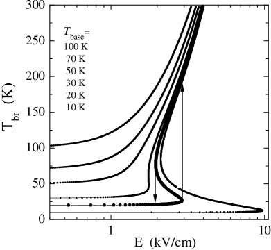
Although in reality depends on the type of substrates, and may vary strongly with temperature, a reasonable qualitative picture of the overheating can be obtained by assuming to have an average, temperature-independent value. Figure 5 illustrates how an actual temperature of a typical LSCO bridge (0.1 m thick, 25 m wide) should change with applied electric field; the calculations are done using the experimental data and taking mW/Kcm. Apparently, as the applied electric field reaches several hundreds V/cm, the actual temperature of the bridge should deviate considerably from the base temperature; this deviation is stronger at higher , where the bridge conductivity and thus the produced power are larger. For low base temperatures, the smooth heating becomes unstable because of a positive feedback: As the bridge is heated, its resistivity drops and the produced power grows much quicker than the heat removal does, causing a thermal instability and a very abrupt increase in temperature by several hundreds degrees (Fig. 5). In fact, for realistic that decreases at high temperatures, the high- branches of the curves in Fig. 5 become almost vertical, so that an applied voltage of several kV/cm would literally burn the sample.
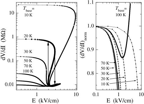
The non-linearity in characteristics, that follows from the calculated Joule overheating, is shown in Fig. 6. It turns out that the differential resistance, , may stay virtually unchanged up to the electric field kV/cm, but it should show a spectacular drop upon further increasing the voltage, as the bridge gets heated by the current. The arrows in Fig. 6 indicate an inevitable switching between the high and low-resistance states accompanied by a hysteresis – the phenomena that are unrelated to any electronic peculiarities, but are governed exclusively by the conventional heating. Upon measuring the characteristics and interpreting the data we therefore should keep in mind the threshold field of kV/cm, where the Joule heating becomes crucial.
One may wonder whether a pulse technique can be helpful in avoiding the overheating problem; thus, it is instructive to estimate the characteristic time for the sample heating. For example, at K the heat capacity per unit length of a bridge (with a cross section of 2.5 m2) can be estimated as m J/Kcm3= J/Kcm. When an electric field of 1 kV/cm is applied to the bridge at 20 K [Fig. 6(a)], the produced power is mW/cm (or merely mW for our 100-m-long bridge). In an equilibrium state, when the heat is removed through the substrate with mW/Kcm, the power mW/cm would cause just a minor overheating by K. However, in the absence of heat removal, this seemingly small power would heat the bridge at a rate of K/s; apparently, the bridge’s temperature should approach its equilibrium value within an extremely short time of s. In the case of thin films, the heat capacity is therefore a poor competitor to the heat conductivity in controlling the overheating rate, and thus the pulse technique can hardly be helpful.
It should be noticed that the above estimates are done for LSCO , while for samples with higher doping the “safe” electric field decreases as a square root of the resistivity; it also decreases with increasing the sample’s cross section, so that bulk samples can be significantly overheated by orders of magnitude smaller electric fields.
III.3 Current-voltage characteristics
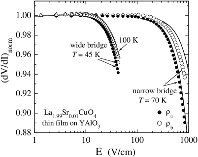
Upon looking for non-linear conductivity features related to the collective charge motion, we have measured the differential resistance of narrow ( m) LSCO bridges by sweeping the bias field up to kV/cm. Measurements were performed at fixed temperatures in the range from 150 K (where has a minimum, see Fig. 2) down to 40 K (where exceeds the minimum value by several times); typical data taken at K are shown in Fig. 7. The characteristics turn out to be perfectly linear, and thus the differential resistance stays unchanged, up to rather high fields of V/cm. Upon further increasing the voltage, the differential resistance goes down, dropping by % as the field approaches 1 kV/cm. However, this resistivity decrease is smooth, without any step-like feature that one would expect for the collective stripe sliding; moreover, it well fits the overheating effect estimated for each bridge using its resistivity and the heat conductivity of the substrate (solid lines in Fig. 7). In order to confirm that the non-linearity emerging at high voltages is caused solely by the Joule heating, we have measured several bridges with different geometries. Since the produced heat scales with the sample’s volume, while the heat removal rate changes rather slowly, the onset of non-linearity in larger bridges should take place at lower electric fields. Figure 7 demonstrates that this is indeed the case: Wide bridges show non-linearity starting already at 10-20 V/cm. Apparently, the obtained data leave little room for any intrinsic non-linear conductivity in LSCO films, at least at moderate electric fields that do not cause significant overheating.
The characteristics measured on LSCO () bridges also show a perfectly linear behavior up to electric fields of V/cm (Figs. 8, 9), that is, as long as the field stays within the “safe” range where the estimated Joule heating is negligible. At higher fields, the data deviate from a constant value, however this deviation clearly traces the temperature dependence of , giving an additional evidence for the overheating mechanism. For example, dependences measured for LSCO () bridges at K – somewhat below the resistivity minimum – exhibit a non-monotonic behavior, also passing through a minimum (Fig. 8). In fact, what we see in the curves is simply an increase of the actual bridge’s temperature , so that is equal to the resistivity . A good quantitative agreement of the data with the fit in Fig. 8 clearly indicates that there is no other source for the non-linear conduction, besides overheating.
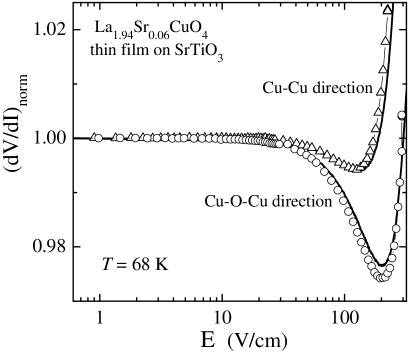
Figure 9 presents the data obtained for LSCO () bridges deposited on LaSrAlO4. Depending on whether the measurements are done at temperatures where is positive or negative (see Fig. 4), the differential resistance increases or decreases with increasing electric field, exactly as expected for the non-linearity originating exclusively from the Joule overheating. No other features could be detected in the curves at any temperature down to the onset of superconductivity at K.
To summarize the experimental observations, we can state that no signs of intrinsic non-linear conductivity are found in LSCO ( and 0.06) thin films when electric fields up to several hundreds V/cm are applied along any crystallographic direction.
III.4 Do the stripes actually exist in cuprates?
Since the performed experiments could not reveal any non-linear feature related to the collective charge motion, a natural question to be asked is whether this negative result can somehow be reconciled with the existence of charged stripes. In fact, the only obvious possibilities are that the charged stripes in LSCO, if actually exist, are either pinned so strongly that available electric fields appear to be too weak to induce their sliding, or they are instead not pinned at all and exhibit a linear fluid-like behavior even at the lowest fields. The latter possibility, however, sounds quite unlikely given the insulating tendency of the resistivity at low temperatures (Fig. 2). We should therefore consider the conditions that may prevent the charge order from being dragged by electric fields; then the limitations imposed by the present result on the picture of stripes in cuprates will become clear.
In general, the electrical conductivity of solids becomes non-linear when electrons accelerated by an applied electric field acquire an energy (where is the hopping distance or mean free path) comparable to other relevant energy scales such as the Fermi energy , the band gap , or ; usually this occurs at very high fields, V/cm. What is specific to charge-ordered systems is that the electric-field effect is integrated over a macroscopic number of electrons being able to move cooperatively. Consequently, the characteristic fields are reduced dramatically, roughly speaking by as many times as the number of electrons involved in the cooperative motion. The observation of a threshold conductivity at small fields thus implies that the following conditions are met: (i) the charge order is stiff enough to keep its phase over a fairly large coherent domain, whose volume contains electrons participating in the CDW; (ii) pinning of such domain by the lattice or impurities is substantially stronger than thermal fluctuations, , otherwise the system exhibits a fluid behavior without any threshold for conduction; (iii) a force exerted by a fairly small electric field on a phase-correlated domain, , can overcome the pinning. In fact, the latter two conditions are also related to the CDW stiffness: Thermal fluctuations become irrelevant for macroscopic domain sizes, and a stiffer CDW is pinned less readily by uncorrelated defects. CDW_rev ; cuprates ; CDW_theo
In inorganic chain compounds such as transition-metal chalcogenides NbSe3, TaS3, or blue bronze K0.3MoO3, the key to spectacular non-linear conductivity phenomena is an extremely large coherence length of the charge order, reaching m. CDW_rev ; CDW_size ; CDW_dom Correspondingly, the threshold field for depinning the CDW is reduced by many orders of magnitude from characteristic single-electron values down to 1-100 mV/cm, CDW_rev ; CDW_thr ; CDW_size ; commen and the features related to the CDW sliding stay sharp up to the CDW-formation temperature, since thermal fluctuations have no impact on macroscopic correlated domains.
The fact that electric fields of several hundreds V/cm are unable to induce non-linear conduction in lightly doped LSCO indicates that the phase-correlated domains here should be much smaller than in chain compounds. Let us roughly estimate how small they should be. According to neutron scattering, the stripes become static at temperatures below 10-30 K, implying the pinning energy per domain to be of the order of several meV. By comparing the work that an electric field would do upon dragging stripes by one lattice constant , , with the pinning energy, one can estimate that electric fields kV/cm would be incapable of depinning phase-correlated domains if they contain electrons. More sophisticated calculations by Morais Smith et al. cuprates predict and a stripe-depinning field in LSCO , V/cm. Whatever the case, the phase coherence in LSCO can hardly exceed lattice constants along the direction of stripes and more than just a few periods in transverse directions. It is worth noting however that the above estimates do not imply the stripes to be fragmented, they only indicate the length scale over which the stripe structure can behave as a stiff object.
Apparently, the charge stripes in cuprates with so short coherence length should look like a “spaghetti” of flexible weakly-interacting strings (Fig. 10), rather than a conventional rigid CDW. The term “electronic liquid crystal” has been coined to describe such unusual state of matter. Kivelson What, however, makes the stripes so different from CDW, and what allows them to be flexible? In 1D chain compounds, the stiffness of CDW comes from its insulating nature: The electronic energy is reduced owing to a gap opening at the Fermi energy, and the CDW period is strictly determined by the Fermi wave number . Consequently, any forced modification of the CDW period would shift the gap away from the Fermi surface, and thus inevitably destroy the CDW. In 2D systems, the metallic state usually survives the CDW formation,CDW_2D and the resulting CDW is much less stiff: it can modify the periodicity and orientation to fit different parts of the Fermi surface. The charged stripes in cuprates have a good reason to be even more flexible; they are formed because holes are expelled from antiferromagnetic domains, while a possible ordering of stripes into a periodic structure is merely a secondary effect. In fact, the stripe’s flexibility originates from the absence of a gap at the Fermi level, which allows the stripes to change their filling (number of holes per unit length) and thus the spacing between adjacent stripes. Moreover, the energy of stripes only weakly depends on their orientation within CuO2 planes, since both vertical and diagonal ones are experimentally observed diag_ver in lightly doped LSCO. This makes it easy for stripes to bend and form kinks, as is sketched in Fig. 10. Needless to say that such “electronic liquid crystals”, where each small fragment slides virtually independently and can adjust itself to the ionic lattice or impurities, should never exhibit any threshold conduction features. In this sense, our observation of linear characteristics gives evidence that if the charge-density modulations actually exist in underdoped cuprates they should be of the electronic liquid-crystal type.
III.5 Implications for other transition-metal oxides
One might wonder whether the absence of threshold conduction in LSCO indicates a fundamental difference of the stripes in cuprates from the charge ordered states in other transition-metal oxides, such as nickelates or manganites. Nature ; Science ; LaSrNiO ; film ; film_perp This may indeed be true, since the charge-ordered nickelates or manganites usually possess much higher resistivity than the layered cuprates do. However, a close analysis of relevant publications shows that there is, in fact, no unambiguous evidence for the collective charge motion in other layered (or 3D) oxides either. The spectacular resistivity switching found in single crystals of manganites, nickelates, or chain cuprates SrCuO2 and Sr2CuO3 always takes place at remarkably similar conditions,Nature ; Science ; LaSrNiO ; SrCuO implying that peculiarities of the electronic and crystal structures of these compounds may not be the key for this phenomenon. Moreover, the observed characteristic threshold field of the order of several kV/cm, and the shape of the characteristics, both are very similar to what should be expected for the heating effects (Fig. 6). In all these experiments, the power dissipation in the low-resistance state was mW; given a rather small heat conductivity of these samples (for example, in manganites kappa_Mn mW/Kcm), this was large enough to overheat the mm-size crystals by K, let alone a much stronger local heating possible for inhomogeneous current flows. Bonch ; hot_spot
Of course, it would be incorrect to attribute the non-linear conductivity in manganites and nickelates entirely to the Joule heating: electronic inhomogeneities inherent in these compounds may set an arrangement of conducting filaments, the flowing current may alter the charge-order domain structure, etc. The problem is, however, that the electric fields required to induce the resistivity switching in layered oxides are clearly out of the “safe” range, and thus a special care should be paid to distinguish an initial coherent charge-order sliding, LaSrNiO if it actually takes place, from the following heating effects that quickly mess everything up. Such problems were often encountered upon measurements of 2D electron systems 2DEG_heat and semiconductors hot_spot ; not_ther as well.
When a high electric field is applied to an insulating sample, a homogeneous current distribution becomes unstable, Bonch and a kind of “spark” may develop along the best conducting path, tending to spread and burn the sample. If, however, the total current flowing through the sample is limited, the spark channel optimizes its size to keep the temperature high enough for providing the required conductivity. A self-optimized channel may collect virtually all the current flowing through the sample,hot_spot ; not_ther rising its density up to A/cm2. density In a sense, such conducting filament inside a crystal is quite reminiscent of our conducting bridges on insulating substrates. As we discussed in Sec. III.2, a power of mW (typical for high-resistivity state SrCuO ; LaSrNiO ) can considerably overheat a bridge, or equivalently, a conducting filament within several microseconds; apparently, the experimentally observed SrCuO ; LaSrNiO switching delays of 1-1000 ms provide more than enough time for the heating process to develop.
To understand whether or not the temperature of conducting filaments actually exceeds significantly the average temperature of crystals, one needs to know the exact geometry of filaments. hot_spot ; not_ther An optical study of Pr0.7Ca0.3MnO3 crystals has shown that a 0.15-mm-long conducting filament expands up to 0.2 mm in diameter as the dissipating power reaches mW. Science For that particular filament geometry and the heat conductivity mW/Kcm (Ref. [kappa_Mn, ]), one can estimate that the overheating must be rather large, K, which alone can induce a resistivity switch. The role of heating becomes more clear when samples with different sizes are compared: In Pr0.7Ca0.3MnO3 thin films, the resistivity switching has been found film_perp to occur at significantly higher fields, V/cm; interestingly, the power dissipation in the low-resistance state of these films still appears to be virtually the same as in single crystals, mW. This power released on the surface of 2500 m2 – exactly as the surface of our bridges (25 m 100 m) – had to overheat the film by K, which well accounts for the observed resistivity drop.
It turns out, therefore, that the non-linear conductivity in layered transition-metal oxides is observed only at very high electric fields where heating effects should become crucial. Consequently, thus far one has insufficient information to conclude whether or not a coherent sliding of stripes (or another charge order) can ever be induced in these compounds. It may well be that the charge ordering in layered oxides is always of the same kind – flexible and readily adjustable to the ionic lattice and impurities.
IV Conclusions
The ubiquity and properties of the charged stripes in high- cuprates still remain an issue. We have tried to induce a coherent sliding of the charged stripes in La2-xSrxCuO4 ( and 0.06) thin films by applying high electric fields up to 100-1000 V/cm, yet observed no non-linear conductivity features, at least as long as the films are not overheated significantly by the flowing current. This result can be reconciled with the existence of charged stripes only if they are very flexible, since the less stiff order is known to be pinned more readily. Simple estimates show that the volume over which the stripes move coherently can hardly include more than holes, implying the stripe fragments are capable of moving virtually independently. Consequently, the self-organized electronic structures in cuprates, and presumably in other layered oxides, should be considered as a kind of “electronic liquid crystal” rather than as a superposition of rigid charge and spin density waves.
Acknowledgements.
We thank K. Segawa for invaluable technical assistance.References
- (1) For review of charged stripes in cuprates, see E. W. Carlson, V. J. Emery, S. A. Kivelson, and D. Orgad, cond-mat/0206217.
- (2) J. M. Tranquada, B. J. Sternlieb, J. D. Axe, Y. Nakamura, and S. Uchida, Nature 375, 561 (1995).
- (3) M. Fujita, K. Yamada, H. Hiraka, P. M. Gehring, S. H. Lee, S. Wakimoto, and G. Shirane, Phys. Rev. B 65, 064505 (2002).
- (4) Y. Ando, A. N. Lavrov, S. Komiya, K. Segawa, and X. F. Sun, Phys. Rev. Lett. 87, 017001 (2001).
- (5) Y. Ando, K. Segawa, S. Komiya, and A. N. Lavrov, Phys. Rev. Lett. 88, 137005 (2002); Y. Ando, A. N. Lavrov, and K. Segawa, Phys. Rev. Lett. 83, 2813 (1999).
- (6) For review of charge-density waves in quasi-1D compounds, see Electronic Properties of Inorganic Quasi-One-Dimensional Compounds, Pt. II, edited by P. Monceau (Reidel, Dordrecht, 1985); G. Grüner, Rev. Mod. Phys. 60, 1129 (1988).
- (7) M. Fujita, H. Goka, K. Yamada, and M. Matsuda, Phys. Rev. B 66, 184503 (2002).
- (8) R. M. Fleming, and C. C. Grimes, Phys. Rev. Lett. 42, 1423 (1979).
- (9) M. M. Fogler, cond-mat/0111001.
- (10) V. J. Goldman, M. Santos, M. Shayegan, and J. E. Cunningham, Phys. Rev. Lett. 65, 2189 (1990); F. I. B. Williams, P. A. Wright, R. G. Clark, E. Y. Andrei, G. Deville, D. C. Glattli, O. Probst, B. Etienne, C. Dorin, C. T. Foxon, and J. J. Harris, Phys. Rev. Lett. 66, 3285 (1991).
- (11) K. B. Cooper, M. P. Lilly, J. P. Eisenstein, L. N. Pfeiffer, and K. W. West, Phys. Rev. B 60, R11285 (1999); K. B. Cooper, J. P. Eisenstein, L. N. Pfeiffer, and K. W. West, cond-mat/0210069.
- (12) M. P. Lilly, K. B. Cooper, J. P. Eisenstein, L. N. Pfeiffer, and K. W. West, Phys. Rev. Lett. 83, 824 (1999); W. Pan, T. Jungwirth, H. L. Stormer, D. C. Tsui, A. H. MacDonald, S. M. Girvin, L. Smrc̆ka, L. N. Pfeiffer, K. W. Baldwin, and K. W. West, Phys. Rev. Lett. 85, 3257 (2000).
- (13) T. Noda, H. Eisaki, and S. Uchida, Science 286, 265 (1999).
- (14) Y. Ando, K. Segawa, A. N. Lavrov, and S. Komiya, cond-mat/0208096.
- (15) G. Blumberg, P. Littlewood, A. Gozar, B. S. Dennis, N. Motoyama, H. Eisaki, and S. Uchida, Science 297, 584 (2002).
- (16) A. Maeda, R. Inoue, H. Kitano, N. Motoyama, H. Eisaki, and S. Uchida, Phys. Rev. B 67, 115115 (2003).
- (17) A. Asamitsu, Y. Tomioka, H. Kuwahara, and Y. Tokura, Nature 388, 50 (1997).
- (18) M. Fiebig, K. Miyano, Y. Tomioka, and Y. Tokura, Science 280, 1925 (1998).
- (19) S. Yamanouchi, Y. Taguchi, and Y. Tokura, Phys. Rev. Lett. 83, 5555 (1999).
- (20) H. Oshima, K. Miyano, Y. Konishi, M. Kawasaki, and Y. Tokura, Appl. Phys. Lett. 75, 1473 (1999).
- (21) J. Sakai, A. Kitagawa, and S. Imai, J. Appl. Phys. 90, 1410 (2001).
- (22) C. Morais Smith, Yu. A. Dimashko, N. Hasselmann, and A. O. Caldeira, Phys. Rev. B 58, 453 (1998).
- (23) P. A. Lee, and T. M. Rice, Phys. Rev. B 19, 3970 (1979).
- (24) V. L. Bonch-Bruevich and S. G. Kalashnikov, Physics of semiconductors (Science, Moscow, 1977).
- (25) D. M. Kroll, Phys. Rev. B 9, 1669 (1974).
- (26) P. J. Thomas, J. C. Fenton, G. Yang, and C. E. Gough, Physica C 341-348, 1547 (2000).
- (27) J. McCarten, D. A. DiCarlo, M. P. Maher, T. L. Adelman, and R. E. Thorne, Phys. Rev. B 46, 4456 (1992).
- (28) H. Sato, A. Tsukada, M. Naito, and A. Matsuda, Phys. Rev. B 61, 12447 (2000).
- (29) S. Komiya, Y. Ando, X. F. Sun, and A. N. Lavrov, Phys. Rev. B 65, 214535 (2002).
- (30) A. N. Lavrov, Y. Ando, S. Komiya, and I. Tsukada, Phys. Rev. Lett. 87, 017007 (2001).
- (31) Y. Ando, A. N. Lavrov, and S. Komiya, to be published.
- (32) A. Maeda, M. Naito, and S. Tanaka, J. Phys. Soc. Jpn. 54, 1912 (1985).
- (33) R. M. Fleming, L. F. Schneemeyer, and D. E. Moncton, Phys. Rev. B 31, 899 (1985).
- (34) S. A. Kivelson, E. Fradkin, and V. J. Emery, Nature 393, 550 (1998).
- (35) J. A. Wilson, Phys. Rev. B 15, 5748 (1977).
- (36) Y. Taguchi, T. Matsumoto, and Y. Tokura, Phys. Rev. B 62, 7015 (2000).
- (37) J. L. Cohn, J. J. Neumeier, C. P. Popoviciu, K. J. McClellan, and Th. Leventouri, Phys. Rev. B 56, R8495 (1997).
- (38) H. W. Jiang, H. L. Stormer, D. C. Tsui, L. N. Pfeiffer, and K. W. West, Phys. Rev. B 44, 8107 (1991).
- (39) D. Adler, H. K. Henisch, N. F. Mott, Rev. Mod. Phys. 50, 209 (1978).
- (40) Note, however, that the current density inside conducting filaments can never be as large as A/cm2 as was suggested in Ref. [EtoH, ] to explain the non-linear behavior in manganites, and thus cannot generate any sizeable magnetic field.
- (41) V. Markovich, E. Rozenberg, Y. Yuzhelevski, G. Jung, G. Gorodetsky, D. A. Shulyatev, and Ya. M. Mukovskii, Appl. Phys. Lett. 78, 3499 (2001); A. K. Debnath, and J. G. Lin, Phys. Rev. B 67, 064412 (2003).