[
Observation of the Mott Transition in VO2 Based Transistors
Abstract
An abrupt Mott metal-insulator transition (MIT) rather than the
continuous Hubbard MIT near a critical on-site Coulomb energy
=1 is observed for the first time in VO2, a strongly
correlated material, by inducing holes of about 0.018 into the
conduction band. As a result, a discontinuous jump of the density
of states on the Fermi surface is observed and inhomogeneity
inevitably occurs. The gate effect in fabricated transistors is
clear evidence that the abrupt MIT is induced by the excitation of
holes.
PACS numbers: 71.27. +a, 71.30.+h
]
In a strongly correlated system, a metal-insulator transition (MIT) near a critical on-site Coulomb energy, =1, has long been controversial in terms of whether the transition is abrupt or continuous in experiments [1-4], although a first-order MIT with temperature was observed by Morin [5]. An abrupt MIT indicates the Mott transition (first order) and a continuous MIT is the Hubbard transition (second order). The MIT breaks down an energy gap, formed by the strongly correlated Coulomb energy, between sub-bands in a main band. Mott first predicted that the abrupt MIT occurs when a lattice constant is larger than a critical value [1]. Brinkman and Rice theoretically demonstrated an abrupt MIT near =1 for a strongly correlated metal with an electronic structure of one electron per atom [6]. Hubbard first derived that, when sub-bands overlap just below , there is a finite minimum density of states (DOS) at the Fermi level, the DOS increases with decreasing , and the system is metallic [7]; this is Hubbard’s continuous MIT. Later, the continuous MIT was confirmed in the infinite-dimensional Hubbard model [2].
Applying an electric field to a two-terminal structure, Kumai measured Ohmic behavior in an organic Mott insulator in a regime, where conduction from nonconduction (insulating behavior) occurs. Through a theoretical consideration based on the Hubbard model, Oka described the Ohmic behavior in terms of a universal Landau-Zener quantum tunneling. Boriskov also observed a similar metallic behavior for VO2 to that measured by Kumai . Thus, on the basis of the metallic behaviors and Oka’s analysis, the MIT just below seems to follow Hubbard’s continuous model. However, considering the abrupt MIT observed in resistance measurement (Fig. 1), an abrupt MIT in the electric field should also be found.
In this letter, we observe an abrupt jump of current (or DOS) at an electric field in a two-terminal structure and measure the gate effect of the jump in a three-terminal device (switching transistor). The abrupt jump is analyzed in terms of an abrupt MIT (Mott transition). Inducing internal hole charges of about 0.018 in hole levels into the conduction band with a source-drain field or a gate field of a fabricated transistor [11] is an effective method of revealing the MIT mechanism. Note that Mott criterion, , is obtained from 0.25, where is the Bohr radius for VO2 [12]. corresponds to about 0.018 of the number of carriers in the half-filled band, when one electron in the cell volume, 59.2210-24 cm3, of VO2 is assumed; the number of electrons is about 1.71022 cm-2.
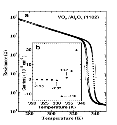
Thin films of a Mott insulator, VO2, with a sub-energy gap of about 1 in the band [13,14], have been deposited on Al2O3 and Si substrates by laser ablation. The thickness of the VO2 films is about 900. The resistance of the film decreases with increasing temperature and shows an abrupt MIT at a transition temperature, =340 K (68∘C) (Fig. 1a). This corresponds with that measured by De Natale [15] and Borek [16]. It was proposed that the abrupt MIT is the structural phase transition from monoclinic below to tetragonal above [5]. The decrease of the resistance up to 340 K indicates an increase of hole carriers, and two kinds of electron and hole carriers coexist near =340 K (Fig. 1b). From 332 to 340 K, the number of carriers is not discernable because of mixing of electrons and holes. We speculate that the number of hole carriers may be the Mott criterion, , at =340 K on the general basis that an exponential decrease of the resistance with temperature in semiconductor physics indicates an exponential increase of carriers. Generally, in oxide materials, there are holes of about 5.510 which corresponds to 0.034 to -band charges . The holes are coupled to optical phonons [17]. In the metal regime above 340 K, the carriers are electrons (Fig. 1).
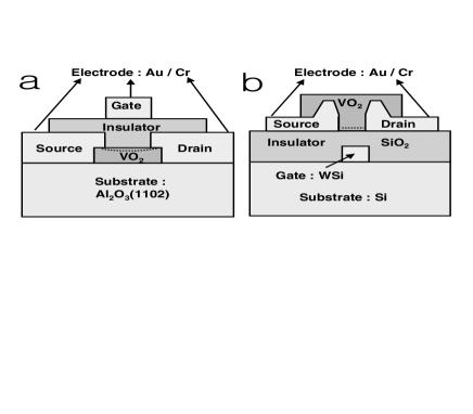
We fabricated transistors to observe the Mott transition. A schematic diagram of the transistors is shown in Fig. 2. Transistor 1 of a channel length, = 3, and a gate width, , was fabricated on Al2O3 substrates by lithography processes (Fig. 2a). A gate insulator of transistor 1 was an amorphous Ba0.5Sr0.5TiO3 (BSTO) which was deposited on the VO2 films. The interface between the VO2 film and the amorphous gate insulator was sharp. A gate-source current, , between the gate and the source for transistor 1 is an order of 10, which indicates that there is sufficient insulation between the gate and the source. Transistors 2 and 3 of a gate length, , and a gate width, , were manufactured on Si substrates. Their structure is shown in Fig. 2b. SiO2 as the gate insulator was thermally treated. It is revealed that an interface between the polycrystal VO2 film and the amorphous SiO2 film is not sharp and complicated, and that the VO2 films are inhomogeneous [20]. However, the SiO2 insulator is strong with respect to a high field and is superior to the BSTO insulator for electronic application. Au/Cr electrodes were prepared for Ohmic contact. WSi is used as gate electrode. Characteristics of the transistors were measured by a precision semiconductor parameter analyzer (HP4156B). To protect transistors from excess current, the maximum current was limited to 20mA.
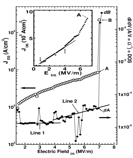
Figure 3 shows the drain-source current density, , vs. the drain-source electric field, , for transistor 1, measured at =0 V (two-terminal structure). and are obtained from the drain-source current and the drain-source voltage, respectively; =(: cross section) and . behavior below point A (Inset of Fig. 3), as observed by Boriskov and Kumai who used an organic Mott-insulator, is linear from 0.8 to 4MV/m, but is nonlinear in the total regime. It was suggested that the linear Ohmic behavior occurs due to an applied field and an induced current [8], not an increase of sample temperature due to leakage current. The Ohmic behavior was well described through a theoretical consideration in terms of a universal Landau-Zener quantum tunneling based on the Hubbard model [9]. However, since holes were observed below 334 K (Fig. 1b), it is asserted that the carriers for the Ohmic behavior are holes and the number of holes is very small. Thus, the Ohmic behavior is not an intrinsic property of metal and may be due to scattering of only a few carriers existing at room temperature by a weak electric field because the density of states (DOS) does not depend on the electric field (line 1 in Fig. 3). Moreover, the nonlinear behavior is semiconduction due to the increase of hole carriers by Zener’s impact ionization and is a doping process wherein of holes are induced by the electric field. This is supported by the fact that the DOS increases exponentially with an increasing electric field (line 2 of Fig. 3). Thus, the VO2 film below point A is regarded as a semiconductor.
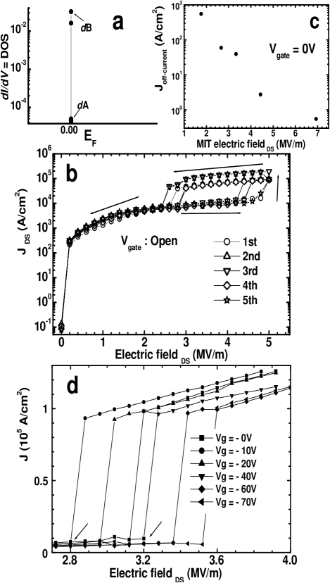
Abrupt jumps of at point A and the DOS at point are shown in Fig. 3. The measured maximum-current density at point B is 2105 A/cm2, which is an order of the current density observable in a dirty metal. Note that the true maximum current density is much higher than , because the measurement was limited to 20mA. The jump of between point A and point B corresponds to a jump of conductivity, , because is and is constant between points A and B; , where is the number of electron carriers (above point A) on the Fermi surface, and is the carrier velocity on the Fermi surface and is constant between points A and B due to constant . This indicates that the number of carriers discontinuously increases, and that the DOS on the Fermi surface jumps from points dA to dB (Fig. 3). The jump of the DOS is a typical behavior of a first-order MIT which was first theoretically derived by Brinkman and Rice [6]. Note that carriers for current measured in semiconductors and metals are on the Fermi surface. Derivatives, , at respective fields correspond to the DOSs on the Fermi surface (Fig. 3). The DOS in Fig. 3 can be expressed in terms of the Fermi level (Fig. 4a). Moreover, hysteresis loops of 5 times for transistor 2 were continuously measured (Fig. 4b), which may be due to the Joule heating and is also evidence of a first-order MIT. The abrupt jump was also measured more than 1,500 times without breakdown in a transistor. Fig. 4d shows Ohmic behavior after jump, which indicates that this phase is metal. Thus, we suggest that the jump at point A is the abrupt MIT (or Mott transition). If Hubbard’s continuous MIT exists, the jump should be not observed and the non-linear behavior with an increasing field in the inset of Fig. 3 should be continuously exhibited from point A to point B in the electron system. However, continuous behavior is not found.
Figure 4c shows the off-current density, , vs. the MIT drain-source electric field, MIT-, at =0 (two-terminal structure). Although =0 , the gate-source currents were very small to be ignored. The off-current is defined as near =0V and =0V (or gate open); other researchers refer to off-current as leakage-current. Data were selected from 5 transistors. MIT- increases with decreasing , which also provides information for revealing the mechanism of the abrupt jump. The off-current is caused by the excitation of holes in impurity levels such as oxygen deficiency. When the number of total holes in the hole levels is given by , where is the number of bound holes in the levels and is the number of holes freed from the levels. decreases with increasing , because is constant. The larger off-current is attributed to the increase of . For the abrupt jump, =0 should be satisfied, where , as predicted by Mott. Hence, the decrease of (increase of ) contributes to the reduction of the MIT-.
Figure 4d shows vs. near the abrupt jump of transistor 3. Its characteristics are as follows. First, the gate effect at =2.8MV/m and =-10V is due to induced holes and occurs suddenly; this indicates attainment of . Second, the MIT- increases with increasing negative gate voltage (or field), which is due to a decrease of the conductivity; s at MIT points can be nearly regarded as constant and . This is due to an increase of hole carriers generated by the negative gate fields and indicates an increase of inhomogeneity (injection of holes to electron system). It was also observed that the MIT- decreases with increasing positive gate voltage when the off-current is large. Third, in the metal (electron system) regime over =0.9104 mA/cm2, Ohmic behavior differs from the Ohmic behavior in the hole system in Fig. 3 and arises from a dirty interface between the polycrystal VO2 film and the amorphous SiO2. The dirty interface causes resistance [20] and is a channel where current flows (Fig. 2b). We suggest that the Ohmic behavior in Fig. 4d is a true metallic characteristic. Finally, the gate induced abrupt MIT reveals that the MIT depends upon the hole carriers in the semiconductor regime, and that inhomogeneity also inevitably arises from hole doping [21].
In conclusion, in the Mott insulator of VO2, MIT near =1 abruptly occurs in company with inhomogeneity through semiconduction as a doping process of internal holes of . This will be observed in all Mott insulators.
We thank Dr. Soo-Hyeon Park at KBSI for Hall-effect measurement, Dr. Gyungock Kim for valuable discussions on the Zener transition, and Dr. J. H. Park for fabrication of Si3N4 films with CVD. HT Kim, the leader of this project, developed the concept, and wrote the paper. BG Chae and DH Youn deposited VO2 and BSTO films, performed the transistor fabrication process including Si based transistors, and measured characteristics. KY Kang prepared the laser-ablation and lithography equipments and generated this project with HT Kim. SL Maeng evaluated transistor characteristics, the shielding measurement system, and the Si3N4 film fabrication.
REFERENCES
- [1] htkim@etri.re.kr, kimht45@hotmail.com
- [2] N. F. Mott (Taylor and Frances Press, 1990).
- [3] X. Y. Zhang, M. J. Rozenberg, and G. Kotliar, Phys. Rev. Lett. 70, 1666 (1993).
- [4] M. Imada, A. Fujimori, and Y. Tokura, Rev. Mod. Phys. 70, 1039 (1998).
- [5] P. Fazekas (World Scientific Press, 1999).
- [6] F. J. Morin, Phys. Rev. Lett. 3, 34 (1959).
- [7] W. F. Brinkman, T. M. Rice, Phys. Rev. B2, 4302 (1970).
- [8] J. Hubbard, 281, 401 (1965).
- [9] R. Kumai, Y. Okimoto, and Y. Tokura, Science 284, 1645 (1999).
- [10] T. Oka, R. Arita, and H. Aoki, cond-mat/0304036.
- [11] P. P. Boriskov, A. A. Velichko, A. L. Pergament, G. B. Stefanovich, and D. G. Stefanovich, Techni. Phys. Lett. 28, 406 (2002).
- [12] S. M. Sze, Chapter 7, (John Wiley and Sons, 1981).
- [13] G. Stefanovich, A. Pergament, and D. Stefanovich, J. Phys.: Condens. Matter 12, 8837 (2000).
- [14] T. M. Rice, H. Launois, and J. P. Pouget, Phys. Rev. Lett. 73, 3042 (1994).
- [15] R. Zimmermann, R. Claessen, F. Reinert, P. Steiner, and S. Hfner, J. Phys.: Condens. Matter 10, 5697 (1998).
- [16] J. F. De Natale, P. J. Hood, and A. B. Harker, J. Appl. Phys. 66, 5844 (1989).
- [17] M. Borek, F. Qian, V. Nagabushnam, and R. K. Singh, Appl. Phys. Lett. 63, 3288 (1993).
- [18] H. T. Kim, H. Minami, and H. Uwe, (Springer-Verlag Press, 1995) p. 169; cond-mat/0303442.
- [19] I. L. Botto, M. B. Vassallo, E. J. Baran, and G. Minelli, Mater. Chem. Phys. 50, 267 (1997).
- [20] K. Sega, H. Kasai, and H. Sakata, Mater. Chem. Phys. 53, 28 (1998).
- [21] D. H. Youn, B. G. Chae, H. T. Kim, J. W. Lee, and K. Y. Kang, unpublished.
- [22] H. T. Kim, (Kluwer Press, 2002), NATO Science Series Vol. II/67, p. 137; cond-mat/0110112.