Spin extraction from a nonmagnetic semiconductor: Tunneling of
electrons from semiconductors into ferromagnets through a modified Schottky barrier
A.M. Bratkovsky and V.V. Osipov
Hewlett-Packard Laboratories, 1501 Page Mill Road, 1L, Palo Alto, CA 94304
Abstract
New efficient mechanism of obtaining spin polarization in
nonmagnetic semiconductors at arbitrary temperutures is described.
The effect appears during tunneling
of electrons from a nonmagnetic semiconductors (S) into ferromagnet (FM)
through a Schottky barrier modified with very thin heavily doped interfacial layer.
We show that electrons with a certain spin projection are extracted from S,
while electrons with the opposite spins are accumulated in S.
The spin density increases and spin penetration depth decreases with current.
]
Spintronics, i.e. the manipulation of spin in solid state devices, opens up
the possibilities for designing ultrafast scaleable devices
[1, 2].
Giant and tunnel magnetoresistance effects in magnetic layered systems
proved to be practically important phenomena [3, 4, 5]. An
injection of spin-polarized carriers into semiconductors is of particular
interest because of relatively large spin-coherence lifetime of electrons in
semiconductors [6] and possibilities for applications in ultrafast
devices and quantum computers [1, 2]. An efficient spin injection
in heterostructures with magnetic semiconductor as a spin source have been
reported in Refs. [7]. However, the Curie temperature of the known
magnetic semiconductors is substantially below room temperature. In Ref.
[8] it was shown that spin injection and extraction in p-n junctions
containing magnetic semiconductors can occur in large magnetic fields (at
least a few Tesla). Fairly efficient spin injection from
ferromagnets (FM) into nonmagnetic semiconductors (NS) has been demonstrated
recently at low temperatures [9]. The attempts to achieve an
efficient room-temperature spin injection from FM into NS have faced
substantial difficulties [10]. Optimal conditions of the spin
injection from FM into NS have been discussed in Refs. [11]. Spin
diffusion and drift in an electric field have been investigated in Refs.
[12]. The spin polarization of photoexcited electrons in NS due to
reflection off a ferromagnet was studied in Refs. [13].
In this paper we consider a ferromagnet-semiconductor junction with very
thin heavily doped semiconductor layer (doped layer) and show that
tunnelling of electrons from a nonmagnetic semiconductor into a
ferromagnet through the doped layer results in formation of highly
spin-polarized electrons in the semiconductor near the interface at room
temperature in absence of an external magnetic field. We assume that the doped layer has the thickness nm, and the
concentration of donors, , satisfying the condition: where
is the elementary charge, ( is the permittivity
of the semiconductor (vacuum), , the Fermi level, the bottom of a semiconductor conduction band, the
height of potential barrier at the ferromagnetic-semiconductor interface.
(Note that for GaAs and Si eV practically for all
metals including Fe, Ni, and Co[14, 9]). The energy band
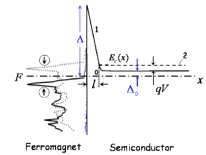
diagram of such a FMS structure includes a spike of
height and thickness (Fig. 1). We consider that
due to a smallness of the electrons can easily tunnel through the spike.
FIG. 1.: Schematic energy diagram of ferromagnet-semiconductor
heterostructure with doped layer in equilibrium (curve 1) and at
bias voltage (curve 2). Here is the Fermi level, the height,
the thickness of the interface potential barrier due to the doped layer, the height of a barrier in the type
semiconductor, the bottom of conduction band in the
semiconductor. The density of states of spin polarized electrons in
ferromagnetic Ni is shown at as an example.
We assume that the electron energy and component
of the wave vector parallel to the interface are conserved during tunneling
through the FM-S interface. The current density of electrons with spin from the semiconductor into the ferromagnet at the interface
(, Fig. 1), which we denote ,
can be written as [15, 5]
(1)
where the Fermi function, the temperature
(in units ), the transmission probability, the
integration includes a summation with respect to a band index, and we
assume that the negative bias voltage is applied to the
semiconductor. We need to
consider, in variance with Refs. [15, 5], that electrons with spin in the semiconductor can be out of equilibrium with their
distribution described by a Fermi function with a quasi-Fermi level . For definiteness, we consider a nondegenerate semiconductor
[16] where a total electron density and a density of electrons with
spin near the interface, , are given by
(2)
Here , is the effective density of states of the semiconductor
conductor band [14], the effective mass of electrons in
the semiconductor, the number of band minima. The analytical
expressions for the transmission probability can be obtained in an effective mass approximation where and are the
velocity and the mass of electron with spin . The potential barrier
(Fig. 1) has a “pedestal” with a height For electron
energies one can approximate the barrier by a triangular shape and find approximately
(3)
where , , , is the
“tunneling” velocity, ( is the component of the
velocity of electrons ( in the semiconductor
(ferromagnet),
(cf. and for a rectangular barrier). The
preexponential factor in Eq. (3) accounts for a mismatch of the
effective masses, and , and the velocities, and , of electrons at the FM-S interface. Note that Eq.
(3) is similar to Eq. (2) of Ref. [5].
In a regime of interest, and [16], Eqs. (1) and (3) can
be written, accounting for a singular energy dependence of the velocity in
the nondegenerate semiconductor as
We have introduced the thermal velocity , and the spin factor . One can see
from Eq. (7) that the current of electrons flowing from nonmagnetic
semiconductors into ferromagnets depends on an electron spin
Note that the present expression for the current is in stark
difference from standard expressions for a current through Schottky
metal-semiconductor contact (see Ref. [14]).
The density of electrons with spin and their spatial distribution
in the semiconductor near the interface is determined by the continuity
equation [14, 12]
(8)
where and the electron
spin-coherence time. The current density of electrons is given by the usual
expression
(9)
where ( are the diffusion constant (mobility) of the electrons, is electric field. Both and are directed along the axis, and , i.e. , the relaxation time of electron momentum in the
semiconductor. From continuity of the total current, , and we have and . Using (8) and (9), we obtain
(10)
where and
are the spin-diffusion and the drift lengths of electrons in a
semiconductor, respectively [12]. The solution of Eq. (10),
satisfying a boundary condition
at is
(11)
The parameter in the above expression is found as follows.
We obtain from Eqs. (7), (11)
(12)
where and we have introduced the effective spin
polarization
(13)
which is the spin polarization of current in a tunneling FM-I-FM structure
[5]. On the other hand, substituting Eq. (11) into Eqs. (9) and using that we find
(14)
One obtains a quadratic equation for
from Eqs. (12) and (14), which has a
unique physical solution, quite accurately represented as
(15)
One can see from (11) and (15) that at very small bias voltage, , and current when the induced spin polarization in the
semiconductor is small,
where . At large voltages and the
current approaching its saturation value the
polarization of electrons reaches the limiting value andnear the interface The spin penetration length
is equal to . Thus, at the electrons with spin are
accumulated, while the
electrons with spin are extracted, from a semiconductor. The penetration
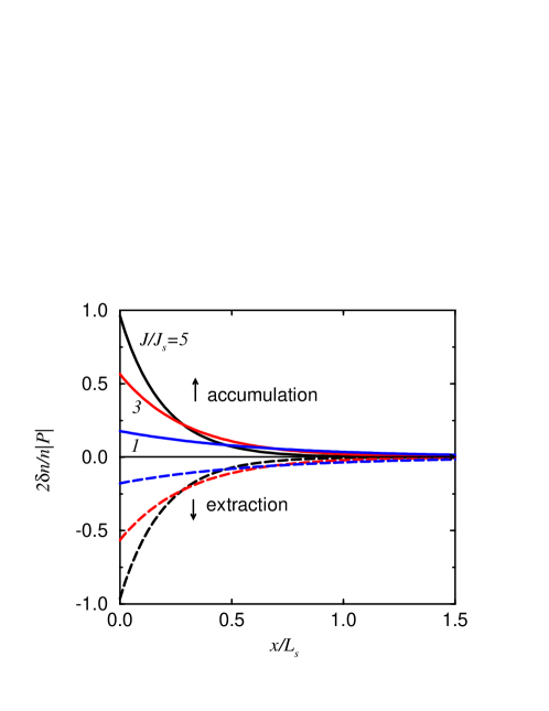
length of the induced spin polarization area decreases as
(Fig. 2). For a typical semiconductor parameters at room temperature cm, s, and m. Thus, when the spin accumulation/extraction at the
interface is and m.
FIG. 2.: Spatial distribution of spin polarized electrons
in the
semiconductor at different currents densities shown next
to the lines.
at
in a structure like the one shown in Fig. 1.
The required spin-relaxation time is obtained from Eq. (7), which
yields at when the -doped layer is very
thin, The corresponding condition reads
(16)
With typical semiconductor parameters at K (
cm2/s, eV,
cm/s [14]) it is satisfied at when the
spin-coherence time s. We notice that
can be ns even at K (e.g. in ZnSe [6]).
We emphasize that , and are all functions of the bias
voltage and . Therefore, by adjusting and
one may be able to maximize a spin accumulation. This can be achieved by
means of electron tunneling through the -doped layer, when the
bottom of the conduction band in a semiconductor is
close to a peak in the density of states of minority electrons in the
elemental ferromagnet like e.g. Ni, , eV [17], as illustrated in Fig. 1.
REFERENCES
[1] S. A. Wolf et al., Science 294, 1488 (2001);
Semiconductor Spintronics and Quantum Computation, edited by D. D.
Awschalom et al. (Springer, Berlin, 2002).
[2] S. Datta and B. Das, Appl. Phys. Lett. 56, 665
(1990); S. Gardelis et al., Phys. Rev. B 60, 7764 (1999); C.
Ciuti et al., Appl. Phys. Lett. 81, 4781 (2002).
[3] M. Baibich et al., Phys. Rev. Lett. 61, 2472
(1988); A. E. Berkowitz et al., ibid. 68, 3745 (1992); J.
S. Mooderaet al., ibid. 74, 3273 (1995).
[4] J. C. Slonczewski, Phys. Rev. B 39, 6995 (1989).
[5] A. M. Bratkovsky, Phys. Rev. B 56, 2344 (1997).
[6] I. Malajovich et al., Nature 411, 770 (2001); I.
Malajovich et al., Phys. Rev. Lett. 84, 1015 (2000); J. M.
Kikkawa and D. D. Awschalom, ibid. 80, 4313 (1998); J. M.
Kikkawa and D. D. Awschalom, Nature 397, 139 (1999); J. M. Kikkawa
et al., Science 277, 1284 (1997); D. Hagele et al., Appl.
Phys. Lett. 73, 1580 (1998).
[7] R. M. Stroud et al., Phys. Rev. Lett. 89,
166602 (2002); M. Tanaka and Y. Higo, ibid. 87, 026602 (2001);
Y. Ohno et al., Nature 402, 790 (1999); R. Fiederling et
al., ibid. 402, 787 (1999).
[8] I. Zutic et al., Phys. Rev. Lett. 88, 066603
(2002).
[9] A. T. Hanbicki et al., Appl. Phys. Lett. 82,
4092 (2003); A. T. Hanbicki et al., ibid. 80, 1240 (2002).
[10] J. Zhu et al., Phys. Rev. Lett. 87, 016601
(2001); P. R. Hammar et al., ibid. 83, 203 (1999); W. Y. Lee
et al., J. Appl. Phys. 85, 6682 (1999); R. Meservey and P.M.
Tedrow, Phys. Rep. 238, 173 (1994).
[11] P. C. van Son et al., Phys. Rev. Lett. 58,
2271 (1987); I. I. Mazin, ibid. 83, 1427 (1999); G. Schmidt et al., Phys. Rev. B 62, R4790 (2000); E. I. Rashba, ibid. 62, R16267 (2000).
[12] M. E. Flatte and J. M. Byers, Phys. Rev. Lett. 84,
4220 (2000); Z. G. Yu and M. E. Flatte, Phys. Rev. B 66, R201202
(2002); Z. G. Yu and M. E. Flatte, ibid. 66, 235302 (2002); J.
D. Albrecht and D. L. Smith, ibid. 66, 113303 (2002).
[13] R. K. Kawakami et al., Science 294, 131 (2001);
R. J. Epstein et al., Phys. Rev. B 65, 121202 (2002); C. Ciuti
et al., Phys. Rev. Lett. 89, 156601 (2002).
[14] S. M. Sze, Physics of Semiconductor Devices (Wiley, New
York, 1981); W. Monch, Semiconductor Surfaces and Interfaces (Springer, Berlin, 1995).
[15] C. B. Duke, Tunneling in Solids (Academic, New York,
1969).
[16] Spin extraction from degenerate highly doped
semiconductors can be achieved at arbitrary temperatures from to K. In this case should be substituted for in all
equations.
[17] V. L. Moruzzi et al., Calculated Electronic Properties
of Metals (Pergamon, New York, 1978).