Measurement of phosphorus segregation in silicon at the atomic-scale using STM
Abstract
In order to fabricate precise atomic-scale devices in silicon using a combination of scanning tunnelling microscopy (STM) and molecular beam epitaxy it is necessary to minimize the segregation/diffusion of dopant atoms during silicon encapsulation. We characterize the surface segregation/diffusion of phosphorus atoms from a -doped layer in silicon after encapsulation at 250∘C and room temperature using secondary ion mass spectrometry (SIMS), Auger electron spectroscopy (AES), and STM. We show that the surface phosphorus density can be reduced to a few percent of the initial -doped density if the phosphorus atoms are encapsulated with 5 or 10 monolayers of epitaxial silicon at room temperature. We highlight the limitations of SIMS and AES to determine phosphorus segregation at the atomic-scale and the advantage of using STM directly.
pacs:
68.35.Dv, 68.35.Fx, 68.37.Ef, 68.49.Sf, 81.15.HiI Introduction
If electronic devices continue to shrink at the same rate as predicted by Moore’s law Moore65 they will within the next 10 - 15 years reach the atomic-scale. The fabrication of silicon-based devices at the atomic-scale requires the ability to control the position of dopant atoms, such as phosphorus with atomic precision. Dopant atoms are usually introduced into the silicon crystal either by ion implantation or by diffusion from highly doped surface layers Sze85 . However, these techniques do not allow for atomically precise control of the position of dopant atoms. An alternative way is to dope a 2D silicon surface and subsequently overgrow the sheet of dopant atoms with epitaxial silicon Oberbeck_APL02 ; O'Brien_PRB01 ; Gossmann85 . One concern with this method is that dopant atoms are known to diffuse at elevated temperature Fahey89 and to segregate during epitaxial silicon growth Nuetzel96 . It is therefore important to monitor the precise position of dopant atoms after high temperature processes such as crystal growth or annealing to ensure segregation and diffusion are kept to a minimum.
Secondary ion mass spectrometry (SIMS) is a commonly used measurement technique to investigate dopant segregation in Si Nuetzel96 ; Friess92 ; Kasper00 . However, it only has the depth resolution of a few nanometers depending on the sample and the sputtering conditions Wilson89 . In the case of phosphorus in Si, additional problems arise with SIMS measurements due to the high mass resolution required to distinguish between 31P (mass 30.9738 webelements ) and 30SiH (mass 30.9816 webelements ). Finally, ion beam mixing during the sputtering process can broaden the dopant profiles thereby influencing any quantitative analysis of dopant segregation.
In this paper, we compare three different methods to quantify the segregation of P atoms in silicon. We use SIMS to study segregation of P atoms in Si at the nanometer scale, Auger electron spectroscopy (AES) for studies at the sub-nanometer scale, and scanning tunnelling microscopy (STM) to measure the segregation and diffusion of phosphorus atoms to the Si surface at the atomic-scale. In each case a Si(001) surface is -doped using PH3 gas as the dopant source followed by an anneal at 600∘C to incorporate the P atoms into the surface. In order to determine the amount of segregation that can occur during Si encapsulation the sheet of dopants is then overgrown with several monolayers (ML) of epitaxial silicon either at room temperature (RT) or 250∘C.
We demonstrate that reducing the silicon growth temperature to room temperature can minimize the segregation length of P in Si to sub-nanometer values, the lowest segregation length values for P in Si shown so far. Subsequent sample annealing, necessary to enhance the structural quality of the low temperature grown epitaxial Si layer, causes the encapsulated P atoms to diffuse to the surface. However, the density of P atoms that reach the surface can be reduced to a few percent of the original P atom density (even after annealing at 500∘C) if silicon encapsulation is performed at RT.
II Experimental
Experiments were performed using an Omicron variable temperature STM with Auger electron spectroscopy and a Si sublimation cell. The base pressure of the two-chamber analysis/growth ultra-high vacuum (UHV) system was 5 10-11 mbar. Phosphorus doped 1 cm Si(001) wafers were cleaved into 2 10 mm2 sized samples, mounted in sample holders, and then transferred into the UHV system. Sample preparation was performed in vacuum without prior ex-situ treatment by outgassing overnight at 550∘C using a resistive heater element followed by direct current heating at the same temperature for several hours. The sample was then flashed for 30 to 60 s to 1150∘C by passing a direct current through the sample. After flashing, the sample was cooled slowly (3∘C/s) from 900∘C to room temperature. The clean sample surface at room temperature was then directly exposed for 15 min to a beam of phosphine (PH3) molecules at a chamber pressure of 10-9 mbar resulting in a surface saturation dosing with phosphine molecules of 0.37 ML Lin99 . An annealing step at 600∘C for 1 min incorporated P atoms into the Si surface and desorbed the H atoms resulting from dissociation of the PH3 molecules giving a total density of 0.25 ML of P atoms at the surface Lin99 .
For the fabrication of -doped samples for SIMS measurements, the sheet of P atoms was then overgrown by an 24 nm thick epitaxial intrinsic Si ( 1 kcm) layer deposited from a Si sublimation cell at a substrate temperature of either 250∘C or RT, and a growth rate of 2 ML/min. Note that RT growth means without intentional sample heating. However, during deposition the sample was radiatively heated by the glowing Si arc used as a sublimation source for Si deposition. The sample temperature is estimated to increase to a few 10∘C above RT during Si deposition. For growth at 250∘C the Si sample was heated by direct current flow through the sample and the sample temperature was controlled by an infrared pyrometer. SIMS measurements were performed on the -doped samples to determine the level of surface segregation of the P atoms during epitaxial silicon overgrowth. Using an ATOMIKA 6500 system with Cs+ primary ion beam the P depth profile was recorded at primary ion energies of 2, 5.5, and 15 keV. As the mass resolution of the ATOMIKA system was not sufficient to distinguish between the masses of 31P and 30SiH, additional SIMS data was acquired at 14.5 keV using a CAMECA SIMS system with a higher mass resolution. The SIMS results were then used to quantify the segregation of phosphorus atoms at the nanometer scale.
In addition, Auger electron spectroscopy and STM were used to study the segregation and diffusion of P atoms at the sub-nanometer scale and atomic-scale, respectively, during epitaxial Si growth and subsequent annealing steps. As before, a Si(001) surface was phosphorus -doped and then overgrown by several monolayers of intrinsic Si at a growth rate of 2 ML/min and at substrate temperatures of either 250∘C or room temperature. After growth the sample was transferred to the analysis chamber where the Auger electron spectroscopy and STM measurements of the density of P atoms segregated to the Si surface were carried out. For Auger electron spectroscopy measurements the sample was then annealed in successive steps at temperatures between 300 and 900∘C in 150∘C steps for 1 min at each step. Auger electron spectroscopy measurements were then performed after cooling down of the sample to RT. For separate STM experiments sample annealing was carried out between 350 and 950∘C in 50∘C steps for 5 s at each step. After each process step the sample surface was investigated at room temperature and the number of P atoms at the surface counted.
III Results and Discussion
III.1 SIMS measurements to study segregation at the nanometer scale
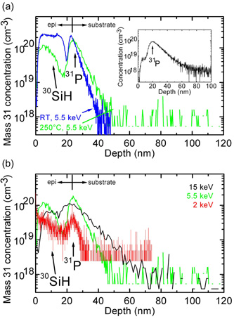
Figure 1 (a) shows SIMS measurements of phosphorus -doped Si(001) samples overgrown at 250∘C and RT, respectively. Using the ATOMIKA system, two distinct mass-31 peaks in the two curves at a depth of 10 and 24 nm were measured. Since it is difficult to distinguish between the 30SiH and 31P peaks additional measurements were carried out using a high mass resolution CAMECA system which displayed only one 31P peak at 20 nm (see inset of Fig. 1 (a)). This additional SIMS data confirms that the broad peak at 10 nm is not due to 31P, but is 30SiH arising from H adsorption at the Si surface. The peak at 24 nm can however, be ascribed to the P -doped layer at the interface between the epitaxial layer and the substrate. The 31P peaks of the samples grown at 250∘C and RT, respectively, display a full width at half maximum (FWHM) of 6 and 4 nm, respectively, for a primary ion energy of 5.5 keV demonstrating the smaller amount of P segregation occurring during RT Si overgrowth. The segregation length Nuetzel96 for P segregation in Si was obtained by fitting the exponential decrease of the P concentration towards the sample surface displayed in Fig. 1 (a), giving values of = 2.3 nm and 1.5 nm for the samples grown at 250∘C and RT, respectively.
Figure 1 (b) highlights the limitations of the SIMS technique. Here we present SIMS measurements of the phosphorus -doped Si(001) sample overgrown at 250∘C for various Cs+ primary ion energies of 2, 5.5, and 15 keV. Note that the apparent reduced P peak height of the 2 keV data results from a quantification of the data using the 5 keV signal as a reference. The P peak is observed to decay into the substrate with the decay length increasing from 1 decade/6.5 nm to 1 decade/20 nm as the primary ion energy is increased from 2 to 15 keV. This variation of the decay length with ion energy is a well-known measurement artefact arising from ion beam mixing, i.e. primary Cs+ ions pushing P atoms further into the substrate during the sputtering process. The SIMS data of the -doped sample shows a FWHM of the 31P peak of 5, 6, and 14 nm for Cs+ primary ion energies of 2, 5.5, and 15 keV, respectively. While it can be seen that measurement artefacts due to ion beam mixing decrease with decreasing primary ion energy, it is also obvious that a small primary ion energy of 2 keV results in low count rates and therefore a stronger noise in the measurement signal and a higher detection limit. Most importantly the variation of the shape of the P peak with primary ion energy demonstrates that the resolution of the SIMS technique is only of the order of a few nm. As a result the segregation of P atoms during growth can only be detected at this level using SIMS highlighting that the technique is not sensitive enough to measure the segregation at the atomic-scale.
III.2 AES measurements to study segregation at the sub-nanometer scale
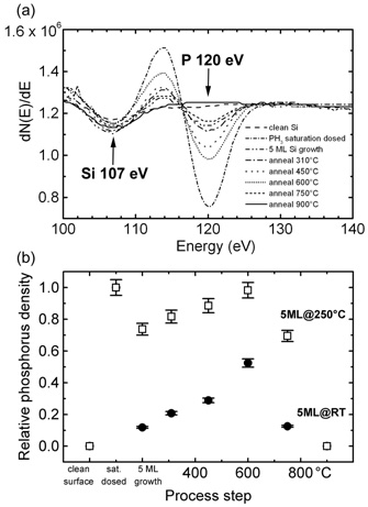
As a consequence we also carried out studies of phosphorus segregation and diffusion at the sub-nanometer scale using Auger electron spectroscopy. Fig. 2 (a) shows Si and P signals at 107 eV and 120 eV Auger electron energies respectively, in the differentiated AES spectrum of the Si sample surface obtained from (i) the clean Si surface, the surface after (ii) PH3 saturation dosing and P incorporation, (iii) 5 ML Si overgrowth at RT, and (iv) various 1 min annealing steps at the temperatures displayed. Note: the intensity of the Auger signal decreases with sample depth and is therefore limited to approx. the first three ML in Si Seah79 .
In order to quantify the amount of P segregation/diffusion we have analyzed the AES data of the integrated spectrum. The number of Auger electrons calculated from the integrated spectrum is directly proportional to the P surface density Jacobson98 . Fig. 2 (b) shows the P density in the first three ML of the sample relative to the P density of the saturation dosed surface from two different growth experiments at 250∘C and RT. If we consider the figure in more detail we see that the clean Si surface after flashing does not show any discernable P concentration, as expected. After P saturation dosing and incorporation of the P atoms, the maximum P density normalized to 1 is visible on the surface giving the largest Auger electron peak at 120 eV. The P surface density then decreases to 0.74 and 0.12 after encapsulation with 5 ML of Si grown at 250∘C and RT, respectively, and increases again with sample annealing at various temperatures up to 600∘C due to P diffusion to the surface. After annealing at 750∘C the P density decreases markedly due to P desorption from the surface as P2 Jacobson98 . Finally after annealing to 900∘C the P peak disappears completely. Phosphorus is still detectable after the 750∘C annealing step as P diffusion from subsurface layers to the surface is still occurring during the anneal.
To calculate the segregation length of P in Si at 250∘C and RT from the AES data we use the relation Nuetzel96
| (1) |
with the incorporation probability and = 0.1358 nm the distance between two subsequent Si(001) monolayers. The relation between the incorporation probability and the segregation length is only valid for first-order kinetic processes and assumes negligible desorption and bulk diffusion. To analyze our data we know that in Fig. 2 (b) we find 74 of P atoms at the surface after 5 ML Si growth at 250∘C. From this value we get an incorporation probability = 0.06. According to equation 1 this value corresponds to a segregation length of = 2.3 nm. For RT growth we find a value of = 0.39 nm. In section D we discuss these values of segregation length obtained using AES measurements in relation to both the values in the literature and to segregation lengths obtained from SIMS and STM measurements. We note however that AES is sensitive to subsurface, non-segregated P atoms and therefore we expect these values to be slightly on the high side of the real . In addition, in the case of RT Si growth due to the high surface roughness of the as-grown surface parts of the surface are covered by less than 5 ML of Si which makes it possible that AES detects non-segregated P atoms in their original lattice positions.
III.3 STM measurements to study segregation at the atomic-scale
Finally in order to gain a better quantitative estimate of the P segregation/diffusion at the atomic-scale we used the STM directly. We imaged the clean Si(001) surface, the surface after PH3 dosing/P incorporation and after Si growth and subsequent annealing steps to determine the density of P atoms at the surface. Annealing of the sample after growth at 255∘C or RT is necessary to flatten the surface in order to identify the characteristic asymmetric appearance of the Si-P heterodimers which form after P incorporation from adsorbed PH3 molecules Oberbeck_APL02 .
Figures 3 (a) - (f) show filled state STM images taken at room temperature of two separate growth experiments. For each experiment STM images of the clean Si(001) surface are shown after initial sample flashing (a); P incorporation (b); Si overgrowth at different temperatures (c); and successive annealing steps for 5 s at 350∘C, 500∘C, and 600∘C (d) - (f). Note that for space reasons only selected STM images of the annealing sequence are shown here. The complete annealing process is however summarized in Fig. 5 (a) and (b). The two experiments only differ in the Si overgrowth step (Fig. 3 (c)): either 5 ML of Si were grown at 255∘C or at RT.
Both experiments started with the preparation of a low defect density clean Si(001) surface, see Fig. 3 (a). The surface was then phosphine dosed and annealed at 600∘C for 1 min to incorporate the phosphorus atoms into the surface and desorb the associated hydrogen Pietsch95 . The resulting image in Fig. 3 (b) shows dimer rows on the Si surface that are strongly buckled due to the high phosphorus density at the surface. After 5 ML growth at 255∘C the surface shows small 2D islands and short Si dimer chains (c). Subsequent annealing of the surface at temperatures of 345 (d), 498 (e), and 600∘C (f) causes the Si surface to flatten due to island coarsening and diffusion of Si atoms to step edges. Simultaneously, the density of bright asymmetric features that result from segregated P atoms forming Si-P heterodimers at the surface increases in accordance with Auger electron spectroscopy data in Fig. 2 (b).
The difference between the two experiments is in the Si growth step (Fig. 3 (c)), where at RT 3D Si islands are formed due to the small mobility of Si atoms on the surface Herman96 . Successive annealing steps flatten the surface as with the 5 ML growth at 255∘C. Interestingly, the Si surface morphology in the different experiments looks very similar for the same annealing temperature, even for the first annealing step at 350∘C for 5 s (d). However, Figs. 3 (d) - (f) clearly show that the density of Si-P heterodimers at the Si surface is much lower for a given anneal temperature if the Si encapsulation occurs at RT compared with 255∘C Si growth.
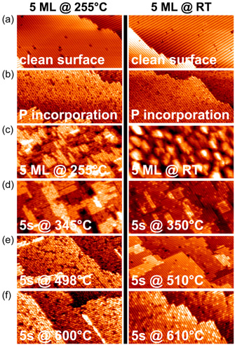
Figure 3 (c) highlights an important limitation in the use of STM to investigate P segregation/diffusion: the high surface roughness that results from low temperature growth, especially room temperature growth, makes identification of Si-P heterodimers at the surface difficult. This occurs for two reasons: firstly, STM images of rough Si surfaces usually have a lower quality compared to images of an atomically flat surface. Secondly, to identify a Si-P heterodimer a sufficient brightness contrast between the heterodimer and the surrounding Si surface is necessary, which can only be obtained for atomically flat surfaces. Therefore, Si-P heterodimers only become clearly visible in our experiments after a short anneal at 350∘C for 5 s. As a consequence the P density at the Si surface after the first anneal is a result of not only P segregation that occurs during growth but also arises from diffusion of P atoms that occurs during the subsequent anneal. Nonetheless it is reasonable to assume that P diffusion, with an energy barrier of 3.66 eV Fahey89 , is negligible for short anneals at such low temperatures. Thus, the P density observed at the surface after the first anneal is most likely a result of P segregation that occurs during Si growth.
To further minimize the surface P density we here also encapsulated the sheet of P atoms with 10 ML, instead of only 5 ML, of Si grown at RT. Figures 4 (a) - (d) show a comparison between the two experiments. For both experiments the surface after Si growth consists of small 3D islands and flattens during subsequent annealing steps as before. As expected, the STM images show that the density of Si-P heterodimers at the Si surface is higher for 5 ML encapsulation compared to 10 ML Si growth.

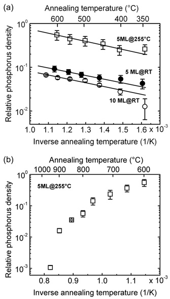
To quantify the density of P atoms at the Si(001) surface observed in the STM images of Figs. 3 and 4 we have counted the number of Si-P heterodimers after each anneal. Figure 5 (a) shows the increase in the density of P atoms at the surface following subsequent annealing steps for the three different experiments. The relative density is obtained by comparison of the phosphorus density after Si growth and sample annealing, with the initial density of incorporated phosphorus atoms after phosphine dosing of the clean Si surface.
If the encapsulation of the sheet of P atoms is undertaken at 255∘C, already 25% of the initial number of phosphorus atoms have segregated during Si growth to occupy surface lattice sites after the first 5 s annealing step at the lowest applied annealing temperature (350∘C), see Fig. 5 (a). After subsequent annealing at 400, 450, 500, 550, to 600∘C nearly 60% of the phosphorus atoms are present at the surface. These results demonstrate that even with a short, low temperature anneal encapsulation of P atoms in epitaxial Si grown at 250∘C results in significant P segregation.
In contrast, if P atoms are overgrown with 5 ML of Si deposited at RT and annealed at 350∘C for 5 s (Fig. 5 (a)), only 5% of the initial number of P atoms are present at the surface (a factor of 5 less). During subsequent annealing at 400, 450, 500, 550, and 600∘C the P density only increases slightly to 10% due to diffusion of phosphorus atoms from subsurface layers to the surface. The reduced density of P atoms at the Si surface compared to the 255∘C Si growth experiment is a direct consequence of the strongly suppressed segregation of P atoms during Si overgrowth at RT. Figure 5 (a) also shows that the surface P density can be further reduced by growth of a thicker Si layer of 10 ML at RT, as seen in the STM images of Figs. 4 (b) - (d). Note that the relative P concentration after various annealing steps obtained from Auger electron spectroscopy measurements shown in Fig. 2 (b) is higher than the values displayed in Fig. 5 (a). This is a direct result of the longer annealing time of 1 min for each step in the AES experiments and the fact that AES also detects subsurface P atoms, highlighting the limitations of this technique.
Figure 5 (b) shows the decrease of the surface phosphorus density for the case of 5 ML Si growth at 255∘C after successive anneals at temperatures between 600 and 950∘C due to phosphorus desorption from the surface. This figure also demonstrates that P atoms are still present at the surface even after annealing for 5 s at 900∘C due to the continual diffusion of P atoms from subsurface layers to the surface.
Using equation 1 we calculate the segregation length of P in Si from the STM data. We know that in Fig. 5 (a) we find about 25 of P atoms at the surface after 5 ML Si growth at 255∘C and the first annealing step at 350∘C. This means that 75 of the P atoms were incorporated. From this value (assuming that only segregation during growth occurred and that the diffusion of P atoms during the first annealing step at 350∘C is negligible) we get an incorporation probability = 0.24. According to equation 1 this value corresponds to a segregation length of = 0.58 nm. For the 5 and 10 ML Si growth at room temperature, the same analysis gives an average segregation length of = 0.34 nm.
III.4 Comparison of segregation length data
In this section we compare the segregation length values obtained from our SIMS, AES and STM data with values from the literature. Segregation length values for P in Si have been published by the Abstreiter group Friess92 ; Nuetzel96 and by Hobart et al. Hobart96 In these studies electrochemical capacitance-voltage profiling (eCV), SIMS Friess92 ; Nuetzel96 , and spreading resistance profiling Hobart96 are used to determine the segregation length at growth temperatures in the range of 320 to 900∘C and growth rates in the range of 0.06 Å/s to 2 Å/s. To compare the literature data with our experimental results we first re-scale the literature data to the growth rate of 0.045 Å/s = 2 ML/min used in our experiments using the relation Nuetzel96
| (2) |
where is the Si growth rate. The growth rate dependence of the segregation length arises from the fact that the growth rate determines the time available for dopant atoms to exchange sites from subsurface to surface lattice sites before they are encapsulated in Si. Since the literature data was obtained at higher Si growth temperatures we have extrapolated their data to RT, as shown in Fig. 6.
From this figure we can see that three observations can be made. Firstly, the experimental values for P segregation in Si determined by the Abstreiter group (Friess and Nützel) and Hobart et al. differ significantly. This difference can result for a number of different reasons, including a difference in the temperature calibration of the growth systems, different measurement techniques (eCV and SIMS vs spreading resistance profiling), and different P doping profiles and doping techniques (MBE growth of P doped layers vs P diffusion) used by the two groups. As a consequence the extrapolation of experimental data from Friess, Nützel, and Hobart et al. to lower temperatures also results in a large difference in the low temperature segregation lengths.
Secondly, there is a noticeable difference in the segregation length values obtained from our SIMS, AES, and STM experiments at the same temperature, see Table 1. The STM values are consistently lower than the respective values determined from SIMS and AES measurements. This can be attributed to limitations of these other techniques, most notably: (i) The depth resolution of the SIMS technique is limited to the nanometer range Wilson89 as a result of the sputtering process, where P atoms in the sample are measured from several monolayers simultaneously. This broadens the P signal leading to an increase in the segregation length obtained. (ii) AES not only detects segregated P atoms at the surface but also detects subsurface, non-segregated P atoms. The analysis of AES data therefore displays a segregation length which is higher than the real . It is anticipated therefore that the segregation lengths obtained from STM measurements are more accurate than both SIMS/AES analysis.
| RT | 250∘C | |
|---|---|---|
| SIMS | 1.50 | 2.30 |
| AES | 0.39 | 2.30 |
| STM | 0.34 | 0.58 |
Thirdly, a final observation that can be made is that our experimental data at these much lower temperatures lies at the limits of the data range expected from extrapolation of the literature values (see the grey area in Fig. 6). There could be two main reasons for this. (i) The sample structures measured are somewhat different: while we used P -doped layers, Nützel Nuetzel96 , Friess Friess92 and Hobart Hobart96 used bulk doped layers. (ii) The strong temperature dependence of the segregation length can mean that a small difference in the temperature calibration of the different growth systems can give significant differences in the segregation length.
Despite the small differences in the segregation length between our data and extrapolated data from the literature, our study shows that low temperature Si encapsulation of P atoms with a few ML of Si, can suppress the segregation of P atoms very effectively. Our results also demonstrate that STM, in contrast to SIMS and AES, allows for a better quantitative determination of the segregation length at the atomic-scale.

Future experiments will focus on STM imaging of the buried phosphorus dopant atoms once they are encapsulated by epitaxial Si overgrowth. Buried dopant imaging has already been demonstrated for boron and arsenic dopants in Si using hydrogen terminated Si(001) surfaces Liu01 . Such a technique would be very important to detect buried P atoms in the Si matrix, not only to allow atomically precise determination of the lateral position, but also the vertical position of the P atoms.
IV Conclusions
We have used SIMS and, for the first time, AES and STM to analyze P segregation/diffusion in Si at very low temperatures (250∘C and room temperature). We show that SIMS is unable to detect segregation lengths of phosphorus atoms in silicon below the nanometer scale. In contrast, AES and STM can be used to monitor the segregation and diffusion of phosphorus atoms in silicon at the sub-nanometer and atomic-scale, respectively. We highlight that Auger electron spectroscopy is limited as a quantitative technique since it detects subsurface, non-segregated P atoms. As a result we demonstrate that STM measurements can be used directly to quantify the surface density of segregated P atoms at the atomic-scale. Using STM we obtained segregation lengths below 1 nm for phosphorus encapsulated in silicon grown at 250∘C and room temperature respectively, which are the lowest values recorded in the literature. Differences between the segregation length obtained and extrapolated experimental data from the literature are accounted for by differences in sample preparation and experimental techniques. These results highlight the effectiveness of room temperature silicon encapsulation to minimize dopant segregation in silicon and how it is possible to quantify this directly using STM.
Acknowledgements.
The authors thank P. Priestley for analysis of STM data. LO acknowledges a Hewlett-Packard Fellowship. MYS acknowledges a Federation Fellowship. This work was supported by the Australian Research Council and the Army Research Office (ARO) under contract number DAAD19-01-1-0653.References
- (1) G. E. Moore, Electronics 38, 114 (1965).
- (2) see e.g. S. M. Sze, Semiconductor Devices - Physics and Technology (John Wiley & Sons, New York, 1985).
- (3) L. Oberbeck, N. J. Curson, M. Y. Simmons, R. Brenner, A. R. Hamilton, S. R. Schofield, and R. G. Clark, Appl. Phys. Lett. 81, 3197 (2002).
- (4) J. L. O Brien, S. R. Schofield, M. Y. Simmons, R. G. Clark, A. S. Dzurak, N. J. Curson, B. E. Kane, N. S. McAlpine, M. E. Hawley, and G. W. Brown, Phys. Rev. B 64, 161401(R) (2001).
- (5) H.-J. Gossmann and L. C. Feldman, Phys. Rev. B 32, 6 (1985).
- (6) P. M. Fahey, P. B. Griffin, and J. D. Plummer, Rev. Mod. Phys. 61, 289 (1989).
- (7) J. F. Nützel and G. Abstreiter, Phys. Rev. B 53, 13551 (1996).
- (8) E. Friess, J. Nützel, and G. Abstreiter, Appl. Phys. Lett. 60, 2237 (1992).
- (9) E. Kasper and M. Oehme, Appl. Phys. Lett. 76, 3573 (2000).
- (10) R. G. Wilson, F. A. Stevie, and C. W. Magee, Secondary Ion Mass Spectrometry (John Wiley & Sons, New York, 1989).
- (11) www.webelements.com
- (12) D.-S. Lin, T.-S. Ku, and T.-J.Sheu, Surf. Sci. 424, 7 (1999).
- (13) M. P. Seah and W. A. Dench, Surf. Interface Anal. 1, 2 (1979).
- (14) M. L. Jacobson, M. C. Chiu, and J. E. Crowell, Langmuir 14, 1428 (1998).
- (15) G. J. Pietsch, Appl. Phys. A 60, 347 (1995).
- (16) M. A. Herman and H. Sitter, Molecular Beam Epitaxy (Springer-Verlag, Heidelberg, 1996).
- (17) K. D. Hobart, F. J. Kub, G. G. Jernigan, and P. E. Thompson, J. Vac. Sci. Technol. B 14, 2229 (1996).
- (18) L. Liu, J. Yu, and J. W. Lyding, IEEE Trans. Nanotechnology 1, 176 (2002).