[
Efficient nonlinear room-temperature spin injection from ferromagnets into semiconductors through a modified Schottky barrier
Abstract
We suggest a consistent microscopic theory of spin injection from a ferromagnet (FM) into a semiconductor (S). It describes tunneling and emission of electrons through modified FM-S Schottky barrier with an ultrathin heavily doped interfacial S layer . We calculate nonlinear spin-selective properties of such a reverse-biased FM-S junction, its nonlinear I-V characteristic, current saturation, and spin accumulation in S. We show that the spin polarization of current, spin density, and penetration length increase with the total current until saturation. We find conditions for most efficient spin injection, which are opposite to the results of previous works, since the present theory suggests using a lightly doped resistive semiconductor. It is shown that the maximal spin polarizations of current and electrons (spin accumulation) can approach 100% at room temperatures and low current density in a nondegenerate high-resistance semiconductor.
pacs:
72.25.Hg, 72.25.Mk]
Spin injection into semiconductors holds promise for the next generation of high-speed low-power electronic devices and perhaps even quantum computing [1, 2, 3, 4]. Among practically important spintronic effects is a giant magnetoresistance in magnetic multilayers and tunnel ferromagnet-insulator-ferromagnet (FM-I-FM) structures [5, 6, 7]. Injection of spin-polarized electrons into semiconductors is of particular interest because of relatively large spin relaxation time [1]. An efficient spin injection in heterostructures with magnetic semiconductor (MS) as a spin source has been reported in Refs. [8]. However, the magnetization in MS usually vanishes or is too small at room temperature. Relatively high spin injection from ferromagnets (FM) into nonmagnetic semiconductors (S) has been recently demonstrated at low temperatures [9], the attempts to achieve an efficient room-temperature spin injection have faced substantial difficulties [10]. Theoretical aspects of the spin injection have been studied in Refs. [11, 12, 13, 14, 15, 16, 17, 18, 19, 20, 21].
Principal difficulty of the spin injection is that the materials in FM-S junction usually have very different electron affinity and, therefore, a high potential Schottky barrier forms at the interface [22], Fig. 1. For GaAs and Si the barrier height eV with practically all metals, including Fe, Ni, and Co, [22, 9] and the barrier width is large, nm for doping concentration cm-3. The spin-injection corresponds to a reverse current in the Schottky contact, which is saturated and usually negligible due to such large and [22]. Therefore, a thin heavily doped S layer between FM metal and S are used to increase the reverse current [22] determining the spin-injection [9, 16, 4]. This layer sharply reduces the thickness of the barrier, and increases its tunneling transparency [22, 4]. Thus, a substantial spin injection has been observed in FM-S junctions with a thin layer [9]. However, the parameters of the structure [9] are not optimal (see below).
A customarily overlooked paradox of spin injection is that a current through Schottky junctions in prior theories depends solely on parameters of a semiconductor [22] and cannot formally be spin-polarized. Some authors even emphasize that in Schottky junctions “spin-dependent effects do not occur” [14].
In earlier works [11, 12, 13, 14, 15, 16, 17, 18, 19, 20] spin transport through FM-S junction, its spin-selective properties, and nonlinear I-V characteristics have not been actually calculated. They were described by various, often contradictory, boundary conditions at the FM-S interface. For example, Aronov and Pikus assumed that a spin polarization of current at the FM-S interface is a constant, equal to that in the FM, and studied nonlinear spin accumulation in S considering spin diffusion and drift in electric field [11]. The authors of Refs. [12, 13, 14, 15, 16] assumed a continuity of both the currents and the electrochemical potentials for both spins and found that a spin polarization of injected electrons depends on a ratio of conductivities of a FM and S (the so-called “conductivity mismatch” problem). At the same time, it has been asserted in Refs. [17, 18, 19, 19, 20] that the spin injection becomes appreciable when the electrochemical potentials have a substantial discontinuity (produced by e.g. a tunnel barrier [18]). The effect, however, was described by the unknown spin-selective interface conductance , which cannot be found within those theories.
We present a microscopic calculation of the spin transport through a reverse-biased FM-S junction which includes an ultrathin heavily doped semiconductor layer (doped layer) between FM and S. We find conditions for the most efficient spin injection, which are opposite to the results of previous phenomenological theories. We show that (i) the current of the FM-S junction does depend on spin parameters of the ferromagnetic metal but not its conductivity, so, contrary to the results [12, 13, 14, 15, 16, 18, 19, 20], the “conductivity mismatch” problem does not arise. We find also that (ii) a spin polarization of current of the FM-S junction strongly depends on the current, contrary to the results [11], and (iii) the highest spin polarization (close to 100%) of both the injected electrons and current can be realized at room temperatures and relatively small currents in high-resistance semiconductors, unlike claimed in Ref. [15], which are of most interest for spin injection devices [2, 3, 4]. We show that (iv) tunneling resistance of the FM-S junction has to be relatively small, which is opposite to the condition obtained in linear approximation in Ref.[18]. We find that (v) the parameters are not constants, as was assumed in [17, 18, 19, 20], but vary with a current in a nonlinear fashion.
The necessary doped layer should be formed at the interface by sequential donor and acceptor doping. The donor and acceptor concentrations, and , and the corresponding thicknesses of the doping profile, and , have to satisfy the conditions:
| (1) |
and where ( nm), , the bottom of conduction band in S in equilibrium, the elementary charge, ( the dielectric permittivity of S (vacuum), the temperature in units of and (see below). Thus, we consider a nondegenerated semiconductor and show that is the case when the most efficient spin injection is realized at room temperatures. A value of can be set by choosing a donor concentration in S,
| (2) |
where the effective density of states and the number of effective minima of the semiconductor conduction band; and the concentration and effective mass of electrons in S [22]. The energy band diagram of such a FM-S junction includes a potential spike of a height and a thickness then a shallow potential well of a thickness and a depth of about followed by low and wide barrier with height in the S, Fig. 1, i.e. is the “mini-well” parameter. Owing to small , the electrons can rather easily tunnel through the spike but only those with an energy can overcome the wide barrier due to thermionic emission, where and is the bias voltage of the reversed-biased FM-S junction. Presence of the mini-well allows to keep the thickness of the spike barrier equal to and its transparency high at voltages (see below).
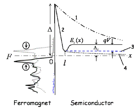
We assume the elastic coherent tunneling, so that the energy , spin and (the component of the wave vector parallel to the interface) are conserved. The current density of electrons with spin through the FM-S junction containing the doped layer (at the point , Fig. 1) can be written as [23, 7]
| (3) |
where is the transmission probability, the Fermi function, the component of velocity of electrons with spin in the ferromagnet in a direction of current; the integration includes a summation with respect to a band index. As distinct from Refs. [23, 7], here we study a strong spin accumulation in the semiconductor. Therefore, we use nonequilibrium Fermi levels, and , describing distributions of electrons with spin in the FM and the S, respectively. This approach is valid when the spin relaxation time is much larger than the relaxation time of electron energy, which is met in practically all semiconductors at room temperature. In particular, the electron density with spin in the S at the FM-S junction is given by
| (4) |
where is a quasi Fermi level at a point , Fig. 1. One can see from (3) that the current if we take , i.e. use the supposition of Refs. [12, 13, 14, 15, 16]. In reality, due to very high electron density in FM metal in comparison with electron density in S, extremely small differ from equilibrium Fermi level for currents under consideration, therefore, as well as in Refs. [23, 7], we can assume that (see below a discussion). Then, we can be rewritten Eq. (3) as
| (5) |
The current (5) should generally be evaluated numerically for a complex band structure [24]. The analytical expressions for can be obtained in an effective mass approximation, . This applies to “fast” free-like d-electrons in elemental ferromagnets [25, 7]. The present barrier has a “pedestal” with a height which is opaque at energies . For we approximate the barrier by a triangular shape and find
| (6) |
where , , is the component of the velocity of electrons in S, , the velocity of electrons in the FM, the “tunneling” velocity, (for comparison, for a rectangular barrier and ).
The preexponential factor in Eq. (6) takes into account a mismatch between effective mass, and , and velocities, and , of electrons in the FM and the S. We consider a bias voltage and . Taking also into account that is nonzero only for the energy when electrons obey a classical statistics, the considered S is nondegenerated. Therefore, using (6) the Eqs. (5) can be written as
| (8) | |||||
Main contributions to the integral come from narrow intervals and . In this region the variables , and are smooth functions and can be replaced by constants with the result
| (10) | |||||
where , and . With the use of Eqs. (2) and (4) we obtain at
| (11) | |||||
| (12) |
We have introduced , the thermal velocity and the main spin factor
| (13) |
which determines the current dependence on materials constants of a ferromagnet.
One can see from Eq. (11) that the total current and its spin components depend on a conductivity of the semiconductor but not the ferromagnet, as in usual Schottky junction theories [22]. However, is proportional to the spin factor and the coefficient , but not the usual Richardson’s factor [22].
Expression (11) is also valid at and determines the spin current from S into FM. At the spin current and results in extraction of spin from nonmagnetic S near the FM-S interface [21].
At the value of and, according to Eq. (11), the spin polarization of the current, , and the spin current at FM-S junction are equal, respectively,
| (14) | |||||
| (15) |
| (16) |
We remind that here where . Thus, depends on bias voltage and differs from that in usual tunneling MIM structures [7], since in the present structure refers to the electron states in FM above the Fermi level, at , i.e. the high-energy equilibrium electrons, which may be highly polarized (see below). Starting with Aronov and Pikus [11], usually one assumes a boundary condition , where
| (17) |
is spin polarization of current in FM. However, there is a spin accumulation in the S and near FM-S boundary in the semiconductor where is a nonlinear function of the current at small current [11] (see also below). Therefore, the greater is , the high is and the smaller is the current [see Eq. (11)]. In other words, a negative feedback is realized which decreases the current polarization and makes it also a nonlinear function of , as we show below. We show that the spin polarizations of the current, , and the electrons, in the semiconductor near FM-S junctions essentially differ and both are low at small bias voltage (and current but increase with the current up to . Moreover, can essentially differ from and can approach 100%.
Indeed, the current in a spin channel is given by the expression [11, 20]
| (18) |
where the electric field; and is the diffusion constant and mobility of the electrons, in considered nondegenerated semiconductors and do not depend on the electron spin . From conditions
| (19) |
we find
| (20) |
Note the injection of spin polarized electrons from FM into S corresponds to a reverse current in the Schottky FM-S junction, i.e. in the considered case and Fig. 1. The spatial distribution of density of electrons with spin in the semiconductor is determined by the continuity equation [11, 15]
| (21) |
With the use of Eqs. (18) and (20), we obtain the equation for . Its solution satisfying a boundary condition at is [11, 20]
| (22) | |||||
| (23) | |||||
| (24) | |||||
| (25) |
where and are the spin-diffusion and the spin drift lengths, respectively. Here defines the degree of spin polarization of nonequilibrium electrons, i.e. a spin accumulation in the semiconductor near the interface,
| (26) |
By substituting (22) into Eqs. (18) and (11), we find that
| (27) |
where . From Eq. (27), one obtains a quadratic equation for with a physical solution, which can be written fairly accurately as
| (28) |
By substituting (28) into Eqs. (11) we find that the total current can be written fairly accurately as
| (29) | |||||
| (30) |
We notice that at a voltage the shallow potential mini-well vanishes and takes the shape shown in Fig. 1 (curve 3). For , a wide potential barrier at remains flat (characteristic length scale nm at cm-3), as in usual Schottky contacts [22]. Therefore the current becomes weakly depending on , since the barrier is opaque for electrons with energies (Fig. 1, curve 4). Thus, Eq. (29) is valid only at and the current at practically saturates at the value
| (31) |
With the using (29) and (24), we obtain from Eq. (28) that spin polarization of electrons at FM-S juction is equal to
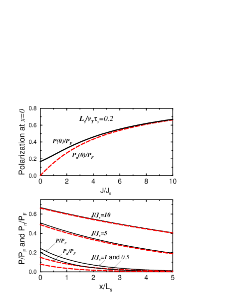
| (32) |
The spin polarization of the current at FM-S interface, according to (11), (27), (24) and (32), is
| (33) | |||||
| (34) |
One can see that strongly differs from at small currents. As expected vanishes with current, the constant of proportionality differs from those obtained in Refs. [11, 15, 17, 19, 20]. At large currents the spin polarization (of electron density) approaches maximum value Unlike the spin accumulation , the current polarization does not vanish at small currents, but approaches a value (see below). Both and approach the maximum only when , Fig. 2. The condition is fulfilled at when According to (30) and (25), the condition for maximal polarization and , can be written as
| (35) |
It can be met most easily for a thin tunneling doped layer with , and semiconductors with a long enough spin-relaxation time. The condition (35) is satisfied for typical parameters at K ( cm2/s, eV, and cm/s) at when s. The spin-coherence time in conventional semiconductors at room temperature is greater than s [1] and can be as long as ns (e.g. in ZnSe [26]). We notice, that when the current spin polarization at small current , since in this case the value for real semiconductor parameters.
Note that the higher the semiconductor conductivity, , the larger the threshold current for achieving the maximal spin injection. In other words, the polarizations and reach the maximum at current in high-resistance low-doped semiconductors rather than in heavily doped semiconductors. Therefore, there is no such thing as a “conductivity mismatch” [14, 18, 19].
According to Eq. (29), at small voltages, the necessary condition can be rewritten as
| (36) |
where is the tunneling contact resistance. Here we have used the Einstein relation for nondegenerate semiconductors. We emphasize that Eq. (36) is opposite to the condition found in Ref. [18] for small currents. Indeed, at small currents only when , i.e. (cf. Ref. [18]). However, at such large tunneling contact resistance the saturation current of the FM-S junction is much smaller than . Therefore, the degree of spin accumulation in the semiconductor is very small, , but this is exactly the characteristic that determines the main spin effects [1, 2, 3, 4]. Note that the conclusion (36) does not depend on the electron concentration in the semiconductor, , and is also valid for heavily doped degenerate semiconductors.
We notice that the quasi Fermi level for electrons with spin in FM extremely small differ from equilibrium Fermi level . It is easy to verify that at current by virtue of smallness of relation , where is electron density in FM metal. Thus, above used assumption is valid.
According to Eq. (13) in the effective mass approximation the spin factor , since usually . In a metal so that where is the density of states of the d-electrons with spin and energy in the ferromagnet. Thus, supposing we find from Eq. (15) . One assumes that the same proportionality between the polarization and the density of states approximately holds in general case of more complex band structures. Note that the polarization of d-electrons in elemental ferromagnets Ni, Co and Fe is reduced by the current of unpolarized s-electrons , where is a factor (roughly the ratio of the number of s-bands to the number of d-bands crossing the Fermi level). Together with the contribution of s-electrons the total polarization is approximately
| (37) |
Such a relation for can be obtained from a usual “golden-rule” type approximation for tunneling current (cf. Refs. [22, 27, 28]). The density of states for minority d-electrons in Fe, Co, and Ni has a larger pick at ( eV) which is much larger than for the majority electrons and for electrons [29] (see Fig. 1). The FM-S junction in Fig. 1 can be tailored to adjust the cutoff energy to the peak in minority electrons. Thus, if one selects then and, according to Eq. (37), the polarization may be close to 100%. (note, that in present case the polarization is negative, ).
We emphasize that the spin injection in structures [3, 9, 10, 11, 12, 13, 14, 15, 16, 17, 18, 19, 20] has been dominated by electrons at the Fermi level and, according to calculation [29], and are such that . We also notice that the condition (35) for parameters of the Fe/AlGaAs heterosructure studed in Refs. [9] ( nm, nm and eV) is satistied when s, that can be fulfilled only at low temperature. Moreover, for the concentration cm-3 lies below where . Therefore, the authors of Refs. [9] were indeed able to observe spin polarization of electrons at low temperatures.
More controlled parameters can be realized in heterostructures in which layer between the ferromagnet and the semiconductor layer made from very thin highly doped -semiconductor with larger electron affinity than the semiconductor. Such heterostructures can be --, -- or -- structures. The , or layer must have the width nm and the concentration cm-3. In this case the superthin barrier forming near the ferromagnet-semiconductor interface is transparent for the electron tunnelling. The barrier height at , or interface is determined by the composition and can be selected as eV. When the donor concentration in , or layer cm-3 the injected electron can not propagate through the low barrier when its width nm.
Summarizing, we showed that (i) the most efficient spin injection at room-temperature occurs in ferromagnetic-semiconductor junctions when an ultrathin heavily doped semiconductor layer (doped layer) satisfying certain conditions is formed between the ferromagnet and the nondegenerate type semiconductor, (ii) the conduction band bottom of the semiconductor, should be close to the peak in the density of minority electron states of elemental ferromagnets Ni, Co and Fe; (iii) the reverse current of such modified Schottky junctions, which determines the spin-injection from ferromagnets into semiconductors, is determined by tunneling and thermoionic emission of spin polarized electrons; (iv) spin injection depends on parameters of both a semiconductor and a ferromagnet, in particular, on velocity of electrons with spin and energy , and a conductivity of the semiconductor (but not the ferromagnet); (v) spin polarizations of current, , and electrons, , in the semiconductor differ from each another and are small at low current; they increase with the total current and reach the maximal possible value only at relatively large current when the spin penetration depth is much larger than the spin diffusion length , and (vi) the smaller the semiconductor conductivity, the lower threshold current for achieving an efficient spin injection. The present theory opens up the way of optimizing the spin-injection structures towards achieving 100% spin polarization in a semiconductor at room temperatures.
We thank D.D. Awschalom, E.I.Rashba, and I. Zutic for useful discussions.
REFERENCES
- [1] S. A. Wolf, D. D. Awschalom, R. A. Buhrman, J. M. Daughton, S. von Molnar, M. L. Roukes, A. Y. Chtchelkanova, D. M. Treger, Science 294, 1488 (2001); Semiconductor Spintronics and Quantum Computation, edited by D. D. Awschalom, D. Loss, and N. Samarth (Springer, Berlin, 2002).
- [2] S. Datta and B. Das, Appl. Phys. Lett. 56, 665 (1990); S. Gardelis, C. G. Smith, C. H. W. Barnes, E. H. Linfield, and D. A. Ritchie, Phys. Rev. B 60, 7764 (1999).
- [3] R.Sato and K. Mizushima, Appl. Phys. Lett. 79, 1157 (2001); X.Jiang, R. Wang, S. van Dijken, R. Shelby, R. Macfarlane, G. S. Solomon, J. Harris, and S. S. P. Parkin, Phys. Rev. Lett. 90, 256603 (2003).
- [4] A. M. Bratkovsky and V. V. Osipov, Phys. Rev. Lett. 92, 098302 (2004); V. V. Osipov and A. M. Bratkovsky, Appl. Phys. Lett. 84, 2118 (2004).
- [5] M.N. Baibich, J. M. Broto, A. Fert, F. Nguyen Van Dau, F. Petroff, P. Etienne, G. Creuzet, A. Friederich, and J. Chazelas, Phys. Rev. Lett. 61, 2472 (1988); A. E. Berkowitz, J. R. Mitchell, M. J. Carey, A. P. Young, S. Zhang, F. E. Spada, F. T. Parker, A. Hutten, and G. Thomas, ibid. 68, 3745 (1992); J. S. Moodera, L.R. Kinder, Terrilyn M. Wong, and R. Meservey, ibid. 74, 3273 (1995).
- [6] J.C. Slonczewski, Phys. Rev. B 39, 6995 (1989).
- [7] A. M. Bratkovsky, Phys. Rev. B 56, 2344 (1997).
- [8] V.V. Osipov, N.A.Viglin, and A.A. Samokhvalov, Phys. Lett. A 247, 353 (1998); Y. Ohno, D. K. Young, B. Beschoten, F. Matsukura, H. Ohno, and D. D. Awschalom, Nature 402, 790 (1999); R. Fiederling, M. Keim, G. Reuscher, W. Ossau, G. Schmidt, A. Waag, and L. W. Molenkamp, ibid. 402, 787 (1999).
- [9] A. T. Hanbicki, B. T. Jonker, G. Itskos, G. Kioseoglou, and A. Petrou, Appl.Phys. Lett. 80, 1240 (2002); A. T. Hanbicki, O. M. J. van’t Erve, R. Magno, G. Kioseoglou, C. H. Li, and B. T. Jonker, ibid. 82, 4092 (2003).
- [10] P. R. Hammar, B. R. Bennett, M. J. Yang, and M. Johnson, Phys. Rev. Lett. 83, 203 (1999); H.J. Zhu, M. Ramsteiner, H. Kostial, M. Wassermeier, H.-P. Schönherr, and K. H. Ploog , ibid. 87, 016601 (2001); W. Y. Lee, S. Gardelis, B.-C. Choi, Y. B. Xu, C. G. Smith, C. H. W. Barnes, D. A. Ritchie, E. H. Linfield, and J.A.C. Bland, J. Appl. Phys. 85, 6682 (1999); T. Manago and H. Akinaga, Appl. Phys. Lett. 81, 694 (2002); A. F. Motsnyi, J. De Boeck, J. Das, W. Van Roy, G. Borghs, E. Goovaerts, and V. I. Safarov, ibid. 81, 265 (2002); H. Ohno, K. Yoh, K. Sueoka, K. Mukasa, A. Kawaharazuka, and M. E. Ramsteiner, Jpn. J. Appl. Phys. 42, L1 (2003).
- [11] A. G. Aronov and G. E. Pikus, Fiz. Tekh. Poluprovodn. 10, 1177 (1976) [Sov. Phys. Semicond. 10, 698 (1976].
- [12] M. Johnson and R.H. Silsbee, Phys. Rev. B 35, 4959 (1987); M. Johnson and J. Byers, ibid. 67, 125112 (2003).
- [13] P. C. van Son, H. van Kempen, and P. Wyder, Phys. Rev. Lett. 58, 2271 (1987); G. Schmidt, G. Richter, P. Grabs, C. Gould, D. Ferrand, and L. W. Molenkamp, ibid. 87, 227203 (2001).
- [14] G. Schmidt, D. Ferrand, L. W. Molenkamp, A. T. Filip and B. J. van Wees, Phys. Rev. B 62, R4790 (2000).
- [15] Z. G. Yu and M. E. Flatte, Phys. Rev. B 66, R201202 (2002).
- [16] J. D. Albrecht and D.L. Smith, Phys. Rev. B 66, 113303 (2002).
- [17] S.Hershfield and H.L.Zhao, Phys. Rev. B 56, 3296 (1997).
- [18] E. I. Rashba, Phys. Rev. B 62, R16267 (2000).
- [19] A. Fert and H. Jaffres, ibid. 64, 184420 (2001).
- [20] Z.G.Yu and M.E. Flatte, Phys. Rev.B 66, 235302 (2002).
- [21] A.M. Bratkovsky and V.V. Osipov, J. Appl. Phys. (2004), to appear; cond-mat/0307656.
- [22] S. M. Sze, Physics of Semiconductor Devices (Wiley, New York, 1981); R. T. Tung, Phys. Rev. B 45, 13509 (1992).
- [23] C. B. Duke, Tunneling in Solids (Academic, New York, 1969).
- [24] S. Sanvito, C.J. Lambert, J.H. Jefferson, and A.M. Bratkovsky, Phys. Rev. B 59, 11936 (1999); O. Wunnicke, Ph. Mavropoulos, R. Zeller, P. H. Dederichs, and D. Grundler, Phys. Rev. B 65, 241306 (2002).
- [25] M.B. Stearns, J. Magn. Magn. Mater. 5, 167 (1977).
- [26] J. M. Kikkawa, I.P. Smorchkova, N. Samarth, D. D. Awschalom, Science 277, 1284 (1997).
- [27] J. G. Simmons, J. Appl. Phys. 34, 1793 (1963); J. G. Simmons, J. Phys. D 4, 613 (1971); R. Stratton, Tunneling Phenomena in Solids, edited by E. Burstein and S. Lundqvist (Plenum, New York, 1969); R. T. Tung, Phys. Rev. B 45, 13509 (1992).
- [28] L. Esaki, Phys. Rev. 109, 603 (1958); M. Julliere, Phys. Lett. 54A, 225 (1975).
- [29] V. L. Moruzzi, J. F. Janak, and A. R. Williams, Calculated Electronic Properties of Metals (Pergamon, New York, 1978); I. I. Mazin, Phys. Rev. Lett. 83, 1427 (1999).