Electromechanical coupling in free-standing AlGaN/GaN planar structures
Abstract
The strain and electric fields present in free-standing AlGaN/GaN slabs are examined theoretically within the framework of fully-coupled continuum elastic and dielectric models. Simultaneous solutions for the electric field and strain components are obtained by minimizing the electric enthalpy. We apply constraints appropriate to pseudomorphic semiconductor epitaxial layers and obtain closed-form analytic expressions that take into account the wurtzite crystal anisotropy. It is shown that in the absence of free charges, the calculated strain and electric fields are substantially differently from those obtained using the standard model without electromechanical coupling. It is also shown, however, that when a two-dimensional electron gas is present at the AlGaN/GaN interface, a condition that is the basis for heterojunction field-effect transistors, the electromechanical coupling is screened and the decoupled model is once again a good approximation. Specific cases of these calculations corresponding to transistor and superlattice structures are discussed.
pacs:
73.21.Ac, 71.20.Nr, 85.30.Tv, 73.20.At, 73.61.Ey, 77.65.LyI Introduction
In previous analyses of the strain in epitaxial layers of AlGaN/GaN, the electrical and mechanical properties of the crystal have been treated as though they are decoupled. Linear elastic theory is assumed to hold, and Hooke’s law is invoked to obtain the relation between the in-plane and axial components of the strain tensor. The standard model decouples the strain tensor from the electric field and enables the separation of the electric field and electronic eigenstate calculations from calculations of the strain field. Historically, there is a solid tradition of using this separability when studying heterostructures of GaAs and associated alloys where the approximation that the strain field is negligibly affected by the electric field is valid.smith
Generally, it is known from thermodynamicsLandau2 that the electrical and mechanical properties of piezoelectric materials are coupled and a simultaneous treatment is called for when the electromechanical coupling is significant. This is the case when the piezoelectric response is large, as it is in AlGaN, especially for high Al fractions. For example, large corrections of the electrostatic and elastic properties have been predicted for AlGaN/GaN transistor structuresjogainew and for free-standing plates of AlNPan1 when a fully-coupled model is used instead of a standard (uncoupled) one.
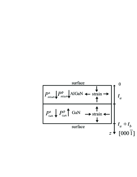
In this paper, we calculate the strain field in a free-standing AlGaN/GaN slab using a fully-coupled model. A free-standing bi-layer slab is chosen as the model structure on which to develop the theory as it can serve as a building block for other, more complicated, structures. For instance, it can be used as a building block for superlattices and quantum wells. In addition, a heterojunction field-effect transistor (HFET) is just a special case of a bi-layer slab in the limit that the GaN layer is much thicker than the AlGaN layer. It will be seen that the fully-coupled strain and electric fields for an HFET can be obtained in this asymptotic limit.
Although the present model is still within the framework of continuum mechanics, it goes beyond the standard continuum elastic theory used in typical strain calculations in semiconductor materials. We obtain the total electric enthalpy for the bi-layer slab and minimize it subject to certain constraints to find both the strain and electric fields. Two constraints are used. One is that the two layers must share a common -plane lattice constant after strain. This lattice constant is unknown at the outset and is deduced only after minimization. The other constraint is set up by the electrostatic potential, and hence the electric field, being forced to satisfy the Poisson equation subject to the boundary conditions at the surface and the common interface. Both the spontaneous and piezoelectric polarizations are included. The effect on the strain and electric fields of a two-dimensional electron gas (2DEG) at the AlGaN/GaN interface, a situation that is essential for channel conduction in the HFET, is also investigated. The model produces expressions for the strain tensor and the electric field in the two layers in closed form.
This paper is organized as follows: In Sec. II, the electric enthalpy for the AlGaN/GaN slab is minimized subject to the constraints derived from the pseudomorphic strain condition and from the Poisson equation. The strain tensor and the electric field are derived in closed form. In Sec. III, the calculated results from the fully-coupled model are contrasted with those from the uncoupled model. The effect on the strain and electric fields of screening from the 2DEG is discussed. The results are summarized in Sec. IV.
II Model description
In the standard strain theory for semiconductor materials, the formal way to calculate the strain field in a generalized strain problem is to minimize the Helmholtz free energyNye ; Landau
| (1) |
in which is the fourth-ranked elastic stiffness tensor, is the strain tensor, and the indices , , , and run over the Cartesian coordinates , , and . Summation over repeated indices is implied throughout. The minimization will, of course, be subject to certain constraints brought about by the boundary conditions at the surfaces and between adjacent materials, as well as any external forces.
In a wide range of semiconductor problems, however, one is concerned with calculating the strain in epitaxial layers grown, at least in principle, pseudomorphically on a thick buffer layer. Typically, the thick layer belongs to, or at least closely resembles, the same crystallographic point group as the epilayers. In this case, a minimization of Eq. (1) is unnecessary, since we can take full advantage of the boundary condition for a free surface which requires that the components of the stress tensor parallel to an outward normal to the surface be zero. For a surface normal to the -axis, this means that , where is the stress tensor. In addition, since the lateral extent of the layers is far greater than their thickness, a one-dimensional (1-D) approximation can be used, wherein for . This condition is equivalent to ignoring the effects of bowing on the local lattice displacement. Under these conditions, the result
| (2) |
is obtained for wurtzite epilayers oriented in the [0001] direction. Here the only unknown is , because a standard approach is to assume that the buffer layer is unstrained and that the epilayer assumes the -plane lattice constant of the buffer, effectively fixing and . Clearly, when , Eq. 2 yields the usual result for the Poisson effect in the case of biaxial strain in an epilayer which is .
The situation for the free-standing bi-layer slab depicted in Fig. 1 in which the two layers are of comparable thicknesses is more complicated, since none of the strain components is known beforehand. To obtain the strain, at least within the standard model, the total mechanical strain energy for the slab must be minimized with respect to subject to the constraints along the interface. There is a further complication in piezoelectric materials such as AlGaN and GaN wherein the electrical and mechanical properties are coupled through the piezoelectric coefficient tensor. Equation (1) is no longer a suitable energy functional for calculating the strain field, since it does not include the electromechanical coupling. Instead, we begin the derivation with the electric enthalpy given byANSI
| (3) |
where E and D are the electric field and electric displacement, respectively, and is the total internal energy given by
| (4) |
in which is the tensor form of the electric permittivity. The electric displacement field components are given by
| (5) |
in which is the piezoelectric coefficient tensor and is the spontaneous polarization.Bernardini The first term in Eq. (5) is recognized as the piezoelectric polarization. The spontaneous polarization is in the direction along the -axis bond. After substitution into Eq. (3), the enthalpy in its final form is
| (6) |
This expression includes the full electromechanical coupling as well as the spontaneous polarization. Differentiating the enthalpy with respect to the strain tensor gives the fully-coupled equation of state
| (7) |
for piezoelectric materials. To obtain the strain and electric fields within a fully-coupled model, Eq. (6) must be minimized with respect to both and subject to the constraints to be discussed shortly for the bi-layer slab of Fig. 1.
Using the Voigt notationNye and expanding Eq. (6), the enthalpy for a wurtzite crystal with the [0001] axis as the principal axis can be written as
| (8) |
where is the electric permittivity assumed here, for simplicity, to be a scalar. The enthalpy for the slab is given by
| (9) |
where and are the thicknesses of the two layers and “a” denotes the AlGaN layer and “b” the GaN layer. It is noted that the elastic and piezoelectric coefficients and the electric permittivity can be substantially different in the two layers. These variations are taken into account in Eq. (9). Because of the rotational symmetry of the slab, and in each layer. The shear terms in the strain tensor, for , turn out to be zero because of the assumption that the strain is piecewise homogeneous. A more realistic assumption would be to expect the strain to diminish away from the interface, resulting in a non-zero that would vary with position along the axis. This situation would be manifested in a bowing of the slab. Such inhomogeneous strains, however, would require a three-dimensional (3-D) numerical calculation that is beyond the scope of the present work.
One of the minimization constraints on Eq. (9) is that the two layers share the same -plane lattice constant which is unknown at the outset. This condition is expressed as
| (10) |
where and are the unstrained -plane lattice of the AlGaN and GaN layers, respectively. Equation (10) presumes ideal growth conditions. Partial relaxation due to dislocations will be the subject of future investigations.
The other constraint is the relationship between the electric and strain fields. This relationship is established in the present work by solving the 1-D Poisson equation given by
| (11) |
where is the electrostatic potential and is the sheet concentration of an ideal 2DEG modeled as a -function at the AlGaN/GaN interface. Equation (11) is solved analytically for subject to the boundary conditions at and and also to the continuity of and the electric displacement across the interface. The general solution of Eq. (11) in each layer is given by
| (12) |
where and are unknown constants. It is evident that there are four unknowns, two in each layer. The ’s are eliminated by enforcing the boundary conditions at and . This condition at the two surfaces presumes that the polarization charge of the materials is terminated by external charges and that the applied bias voltage is zero. Further, it ensures that the electric field in the free space above and below the slab is zero, a reasonable and physically plausible result. The relationship between the two ’s is established from the continuity of the electric displacement and is obtained by integrating Eq. (11) across the interface (see Fig. 1) as follows:
| (13) |
From Eqs. (12) and (13), the relation between the ’s in the respective layers is given by
| (14) |
From Eq. (14) and from the continuity of at , we can solve for all of the remaining unknowns.
With the electrostatic potential now known in terms of the, as yet, undetermined strain tensor, the electric fields in the two layers are then given by
| (15) |
and
| (16) |
where . Equation (9) can be readily minimized with respect to and subject to the constraints expressed in Eqs. (10), (15), and (16) using commercial symbolic-mathematical programs. For convenience, we have also formulated the problem in the form of a matrix equation of the form
| (17) |
in which the matrix elements are obtained by differentiating the energy functional with respect to the unknown strain components. The constraints are already built into Eq. (17) by eliminating , , and from Eq. (9). Equation (17) can be solved either symbolically or numerically. We have provided the symbolic solution as an auxiliary item.EPAPS Appendix A lists the matrix elements.
The fully-coupled model described above reproduces the strain tensor from the standard model in the limit that the piezoelectric stress tensor is set to zero. The results are as follows:
| (18) |
and
| (19) |
for the AlGaN layer and
| (20) |
and
| (21) |
for the GaN layer where the constant factor is defined as
| (22) |
It is further seen from Eqs. (18)–(21) that in the limit , the well-known uncoupled result for the axial strain in an epitaxial AlGaN layer pseudomorphically strained on a thick GaN buffer is recovered:
| (23) |
In this limit, the strain in the GaN layer is reduced to zero, at least ideally, as the thick GaN layer serves as a fixed anchor. The uncoupled electric field in the AlGaN layer in this limit then becomes
| (24) |
We can also extract the fully-coupled results for the strain and electric fields in the limit , i.e. the usual HFET configuration, and compare them with the uncoupled results. In this case, fully-coupled axial strain in the AlGaN layer is given by
| (25) |
and the fully-coupled electric field by
| (26) |
In Eqs. (23), (24), (II) and (26), takes the asymptotic limit as . The first term in Eq. (II) is the result from the standard model. The other two terms are due to electromechanical coupling.
It is worth pointing out that the foregoing results also apply to a free-standing AlGaN/GaN superlattice in which the slab of Fig. 1 forms a period of the superlattice. This outcome follows from enforcing the pseudomorphic boundary condition throughout the entire cross-section of the slab, i.e. for all . In turn, this result is a consequence of the simplifying assumption made at the outset that for . In addition, the electrostatic potential will be subject to periodic boundary conditions at and . We can assume without loss of generality that the potential in the superlattice case can be set to zero at the two ends, as we have done in the present case. A non-zero potential at the two ends in the periodic system simply represents a rigid shift of the potential distribution function and does not change the electric field. Thus a superlattice formed from a stack of slabs discussed in the present work will have identical strains and electric fields within each period as obtained for our model structure.
III Results and discussion
Table 1 shows the material parametersBernardini ; Wright ; Yim ; Maruska ; Tsubouchi ; Shur1 ; Chin used in the calculations. The signs of the polarization parameters are defined in relation to the [0001] direction: a negative sign means that the vector is in the direction.
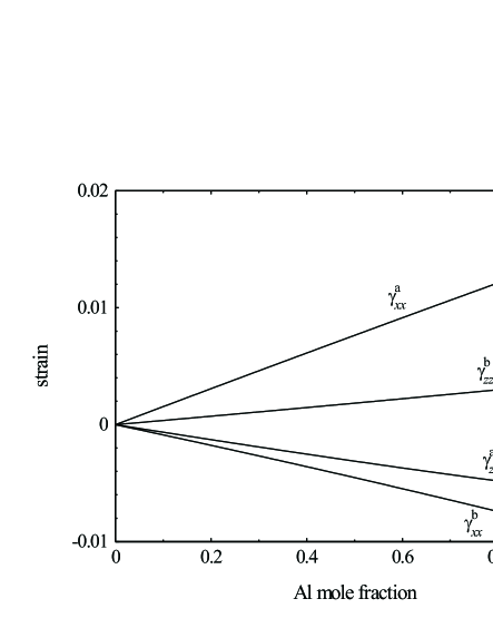
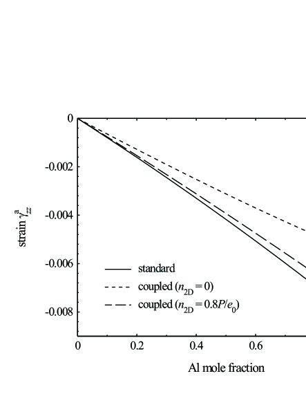
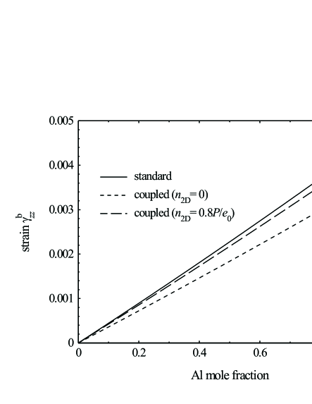
For the model structure of Fig. 1, we choose = 300 Å and = 500 Å. The 300 Å AlGaN layer is typical of most high-power HFETs. It is recognized that the GaN layer used in the model structure is much thinner than that permitted by current technology. For example, using a laser lift-off process and growth via metal-organic chemical vapor deposition (MOCVD), free-standing layers of nitrides can be produced successfully only for relatively thick layersKelly in the vicinity of 5 m. The free-standing layers are even thicker for epilayers grown by hydride vapor phase epitaxy (HVPE), reaching between 250 – 300 m.Kelly2 ; Darak The fully-coupled model presented herein is quite general and, as shown in Sec. II, can readily reproduce the results for thick GaN. Figure 2 shows the calculated strain tensor as a function of the Al fraction using the fully-coupled model for a model structure that is depleted, i.e. . Following standard convention, a positive sign indicates dilation and a negative sign contraction. Unlike the situation of a AlGaN layer on a semi-infinite GaN buffer, both layers are now strained, with the in-plane strain tensile in the AlGaN layer and compressive in the GaN layer.
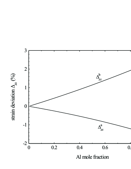
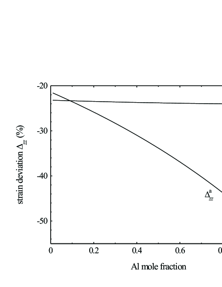
Next we examine the deviation between the fully-coupled and uncoupled models for a depleted slab. This deviation is defined as
| (27) |
where is or , the superscript “a” or “b” refers to a particular layer, and is given by the solution to Eq. (17) for the coupled case and by Eqs. (18) – (21) for the uncoupled case. The calculated results are shown in Figs. 3 and 4 for the in-plane and out-of-plane strains, respectively. It is seen from Fig. 3 that the deviation for is quite small. A possible reason is that the electromechanical coupling of into the equation of state [Eq. (7)] occurs through the piezoelectric coefficient which is much smaller than , as seen from Table 1. The electromechanical coupling of into the equation of state is through which is quite large, especially for AlN. It is clear that the error in the calculated strain along the growth axis is quite significant, reaching 30 % in the AlGaN layer for a mole fraction of 0.3. This error will, in turn, have a significant impact on the calculation of electronic and optical properties that depend on accurate knowledge of the strain. Some examples of such quantities include the eigenstates and the complex dielectric function of the slab.
So far it has been assumed that the slab is depleted with the only charge present being a fixed space charge given by
| (28) |
where and are the piezoelectric polarizations
| (29) |
and
| (30) |
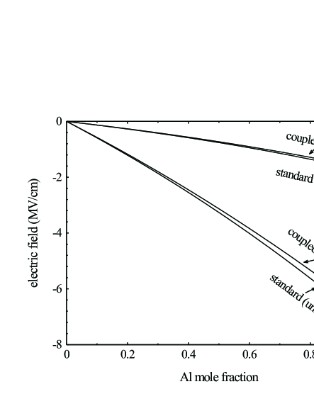
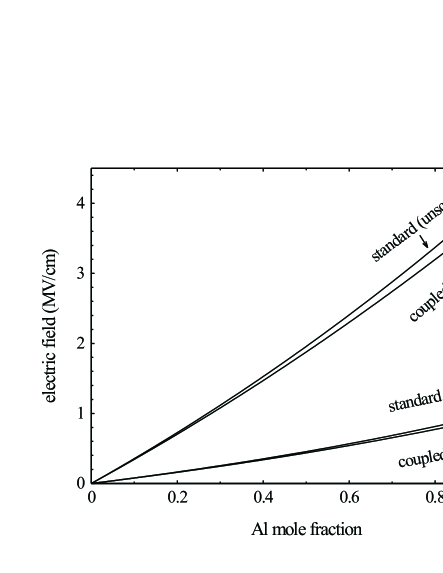
For a cation-faced structure, the standard growth orientation for most HFETs, is positive.Ambacher1 Depending on the growth and surface conditions, donors may be present and may contribute free electrons to the interface. Under certain conditions, the space charge may be partially screened by a 2DEG. For instance, using our own self-consistent Schrödinger-Poisson model,hfetcharge we find that the 2DEG is almost 90 % of the magnitude of the fixed space charge. We assume, conservatively, that and examine the effect of free-electron screening on the electromechanical coupling. Figures 5 and 6 show and , respectively, calculated using the standard and coupled models. The in-plane strains are not shown, since the effect of electromechanical coupling on the in-plane strain components is weak. It is evident from the calculated strains that the effect of coupling is to reduce the magnitude of the strains relative to those of the standard model, especially when the structure is depleted. This result is not surprising, since we would expect the piezoelectric fields to induce forces to oppose any applied forces such as those due to the pseudomorphic interface condition. Another result that is evident from Figs. 5 and 6 is that the 2DEG screening brings the strains of the coupled model closer to those of the standard model. As will be seen shortly, the effect of screening is to reduce the built-in electric fields. This, in turn, will reduce the electromechanical coupling, as seen from Eq. (7).
Figures 7 and 8 show the calculated electric fields in the AlGaN and GaN layers, respectively, using the standard and coupled models. These fields help to explain, in part, the large deviation of the standard strain fields from their coupled counterparts. As an example, for a Al fraction of 0.3, the electric field in the AlGaN layer is about 2 MV/cm, provided that the structure is depleted. Such a large field, if present, will give rise to a strong electromechanical coupling and, therefore, a large discrepancy between the standard and coupled models. When there is a 2DEG, however, the large space charge that gives rise to the electric field is partially neutralized, depending on the magnitude of the 2DEG. For , the field in the AlGaN layer is reduced to about 0.4 MV/cm for a Al fraction of 0.3. Evidence for the smaller field is seen in recent photoreflectance (PR) measurementsGoldhahn ; Shokh on AlGaN/GaN heterostructures in which barrier fields in the vicinity of 0.3 MV/cm were reported for 250 Å thick barriers with Al fractions in the range 0.06 – 0.1. An electric field of opposite sign occurs in the GaN layer with similar trends between the coupled and standard models. Its magnitude is decreased with the thickness of the GaN layer. It is recognized that the calculation of the electric field in the GaN layer is more involved than the classical model presented here allows. The formation of the notch in the conduction band edge in which the 2DEG resides is reproducible only within the scope of a quantum-mechanical calculation. In spite of approximations used, the calculated fields shown here appear to be quite plausible.
IV Summary and Conclusions
In summary, a fully-coupled electromechanical model has been presented for the strain and electric fields in a free-standing bi-layer AlGaN/GaN slab. The electric enthalpy of the slab, with contributions from the piezoelectric and spontaneous polarizations, is minimized subject to the constraints imposed by the pseudomorphic interface condition and the Poisson equation. Closed-form expressions for the strain components and electric field in each layer are obtained. The results for the bi-layer system are also appropriate for freestanding binary superlattices with negligible bowing. Large discrepancies between the standard and coupled models are found for depleted structures due to large built-in electric fields. The electric fields are reduced when the polarization-induced space charge is screened by a 2DEG. As a consequence, the discrepancy between the standard and coupled models is reduced when a 2DEG is present.
Acknowledgements.
The work of BJ was partially supported by the Air Force Office of Scientific Research (AFOSR) and performed at Air Force Research Laboratory, Materials and Manufacturing Directorate (AFRL/MLP), Wright Patterson Air Force Base under USAF Contract No. F33615-00-C-5402.Appendix A Matrix solution of the strain field
The matrix elements required to solve Eq. (17) are given in this appendix. As before, “a” refers to the AlGaN layer and “b” to the GaN layer.
| (31) |
| (32) |
| (33) |
| (34) |
| (35) |
| (36) |
| (37) |
| (38) |
| (39) |
| (40) |
| (41) |
and
| (42) |
References
- (1) D. L. Smith and C. Mailhiot, Rev. Mod. Phys. 62, 173 (1990).
- (2) L. D. Landau, E. M. Lifshitz, and L. P. Pitaevskii, Electrodynamics of Continuous Media, 2-nd ed. (Pergamon Press, Oxford, 1984).
- (3) B. Jogai, J. D. Albrecht, and E. Pan, cond-mat/0306297 (11 Jun 2003) .
- (4) E. Pan and B. Yang, Proc. of the 4th Int. Conference Nonlinear Mech., Shanghai, pp. 479-484 (2002).
- (5) J. F. Nye, Physical Properties of Crystals – Their representation by Tensors and Matrices (Clarendon Press, Oxford, 1985).
- (6) L. D. Landau and E. M. Lifshitz, Theory of Elasticity, 3-rd ed. (Pergamon Press, Oxford, 1986).
- (7) ANSI/IEEE Std 176-1987, IEEE Standard on Piezoelectricity.
- (8) F. Bernardini, V. Fiorentini, and D. Vanderbilt, Phys. Rev. B 56, R10024 (1997).
- (9) See EPAPS Document No. [number will be inserted by publisher ] to view the full analytic solution.
- (10) A. F. Wright, J. Appl. Phys. 82, 2833 (1997).
- (11) W. M. Yim, E. J. Stofko, P. J. Zanzucchi, J. I. Pankove, and M. Ettenberg, J. Appl. Phys. 44, 292 (1973).
- (12) H. P. Maruska and J. J. Tietjen, Appl. Phys. Lett. 15, 327 (1969).
- (13) K Tsubouchi, K. Sugai, and N. Mikoshiba, IEEE Ultrason. Symp. 1, 375 (1981).
- (14) M. S. Shur, A. D. Bykhovski, and R. Gaska, MRS Internet J. Nitride Semicond. Res. 4S1, G1.6 (1999).
- (15) V. W. L. Chin, T. L. Tansley, and T. Osotchan, J. Appl. Phys. 75, 7365 (1994).
- (16) M. K. Kelly, O. Ambacher, R. Dimitrov, R. Handschuh, and M. Stutzmann, Phys. Stat. Sol. (a) 159, R3 (1997).
- (17) M. K. Kelly, R. P. Vaudo, V. M. Phanse, L. Gorgens, O. Ambacher, and M. Stutzmann, Jpn. J. Appl. Phys. 38, L217 (1999).
- (18) V. Darakchieva, T. Paskova, P. P. Paskov, B. Monemar, N. Ashkenov, and M. Schubert, Phys. Stat. Sol. (a) 195, 516 (2003).
- (19) O. Ambacher, B. Foutz, J. Smart, J. R. Shealy, N. G. Weimann, K. Chu, M. Murphy, A. J. Sierakowski, W. J. Schaff, L. F. Eastman, R. Dimitrov, A. Mitchell, and M. Stutzmann, J. Appl. Phys. 87, 334 (2000).
- (20) B. Jogai, J. Appl. Phys. 91, 3721 (2002).
- (21) R. Goldhahn, C. Buchheim, S. Shokhovets, G. Gobsch, O. Ambacher, A. Link, M. Hermann, M. Stutzmann, Y. Smorchkova, U. K. Mishra, and J. S. Speck, Phys. Stat. Sol. (b) 234, 713 (2002).
- (22) S. Shokhovets, R. Goldhahn, G. Gobsch, O. Ambacher, I. P. Smorchkova, J. S. Speck, U. Mishra, A. Link, M. Hermann, and M. Eickhoff, Mat. Res. Symp. Proc. 743, L3.57.1 (2003).
| Material | (Å) | ||||||||
|---|---|---|---|---|---|---|---|---|---|
| AlN | 396111Reference Wright, . | 137111Reference Wright, . | 108111Reference Wright, . | 373111Reference Wright, . | 3.112222Reference Yim, . | 0.58444Reference Tsubouchi, . | 1.55444Reference Tsubouchi, . | 0.081666Reference Bernardini, . | 8.5777Reference Chin, . |
| GaN | 367111Reference Wright, . | 135111Reference Wright, . | 103111Reference Wright, . | 405111Reference Wright, . | 3.189333Reference Maruska, . | 0.36555Reference Shur1, . | 1555Reference Shur1, . | 0.029666Reference Bernardini, . | 10777Reference Chin, . |