Design of realistic switches for coupling superconducting solid-state qubits
Abstract
Superconducting flux qubits are a promising candidate for solid-state quantum computation. One of the reasons is that implementing a controlled coupling between the qubits appears to be relatively easy, if one uses tunable Josephson junctions. We evaluate possible coupling strengths and show, how much extra decoherence is induced by the subgap conductance of a tunable junction. In the light of these results, we evaluate several options of using intrinsically shunted junctions and show that based on available technology, Josephson field effect transistors and high-Tc junctions used as -shifters would be a good option, whereas the use of magnetic junctions as -shifters severely limits quantum coherence.
pacs:
74.50.+r, 85.25.-j, 03.67.Lx, 03.65.YzQuantum computation promises qualitative improvement of computational power as compared to today’s classical computers. An important candidate for the implementation of a scalable quantum computer are superconducting qubits Makhlin ; orlando . After experimental demonstration of basic features e.g. in flux qubits Caspar ; Chiorescu , the improvement of the properties of such setups involves engineering of couplings and decoherence, see e.g. EPJB .
To perform universal quantum computation with a system of coupled qubits it is very much desirable to be able to switch the couplings (although there are in principle workarounds untunable ). It has already been described that for flux qubits, this can be achieved by using a superconducting flux transformer interrupted by a tunable Josephson junction orlando , i.e. a superconducting switch, as shown in Fig. 1. The primary and most straightforward proposal for the implementation of this switch is to use an unshunted DC-SQUID based on tunnel junctions utilizing the same technology as for the qubit junctions. Although this holds the promise of inducing very little extra decoherence, it suffers from two practical restrictions: i) the SQUID loop has to be biased by exactly half a flux quantum in the off-state and ii) the external control parameter is a magnetic flux, which introduces the possibility of flux cross-talk between the qubits and the switch. The combination of i) and ii) implies that even small flux cross-talk will severely perturb the off-state of the switch.
This can be avoided by using different switches: A voltage-controlled device such as a Josephson Field Effect Transistor (JoFET) richter or an SNS-Transistor completely avoids the cross-talk problem. As an intermediate step Blatter , one can improve the SQUID by using a large -Junction, in order to fix the off-state at zero field. Such -junctions can be found in high-Tc systems hightc or in systems with a magnetic barrier sfs . All these junctions are damped by a large subgap conductance because they contain a large number of low-energy quasiparticles.
In this letter, we quantitatively evaluate the coupling strength between two qubits coupled by a switchable flux transformer. We evaluate the strength of the decoherence induced by the subgap current modeled in terms of the RSJ model. Based on this result, we assess available technologies for the implementation of the switch.
We start by calculating the strength of the coupling between the two qubits without a switch and then show how it is modified by the presence of the switch. From Fig. 1 and the law of magnetic induction we find the following equations for the flux through qubit 1 and 2 induced by currents in the qubits and the flux transformer
| (10) |
where is the self-inductance of the qubits (assumed to be identical), is the mutual inductance between the transformer and the qubits and the mutual inductance between the qubits is assumed to be negligible. The fluxes in Eq. (10) are the screening fluxes in the transformer and the two qubits, i.e. the deviations from the externally applied values. Henceforth, we abbreviate Eq. (10) as . These formulas are general and can be applied for any flux through the transformer loop. It is most desirable to couple zero net flux through the device, which can be achieved by using a gradiometer configuration tinkham . For this gradiometer case, we get , which we might insert into (10) and find for the inductive energy
| (11) |
The terms resulting from the off-diagonal elements of (10) can directly be identified as the interqubit coupling strength which enters the Ising-coupling described in Refs. orlando ; PRA . Note, that the dynamics of the qubit flux is dominated by the Josephson energies orlando , to which the diagonal term is only a minor correction.
We now introduce the tunable Josephson junction into the loop. Using fluxoid quantization, we rewrite the Josephson relation tinkham and insert it into eq. (10). The resulting nonlinear equation can be solved in the following cases: i) If (“on” state of the switch) we find with This can be understood as an effective increase of the self-inductance of the loop by the kinetic inductance of the Josephson junction at zero bias. ii) In the case , “off” state, the circulating current is close to the critical current of the switch, hence the phase drop is and we find an analogous form with , i.e. at low the coupling can be arbitrarily weak due to the enormous kinetic inductance of the junction close to the critical current.
We now turn to the discussion of the decoherence induced by the subgap conductance of the tunable junction. The decoherence occurs due to the flux noise generated through the current noise from the quasiparticle shunt. Hence, both qubits experience the same level of noise. The decoherence of such a setup has been extensively studied in Ref. PRA as a function of the environment parameters. In this letter, we evaluate these environment parameters for our specific setup.
We model the junction by the RSJ-model for a sound quantitative estimate of the time scales even though the physics of the subgap conductance is usually by far more subtle than that. We evaluate the fluctuations of the current between two points of the flux transformer loop sketched in figure 1. is the geometric inductance of the loop, is the Josephson inductance characterizing the Josephson contact and is the shunt resistance. The correlation is given by the fluctuation-dissipation theorem where is the admittance of the effective circuit depicted in Fig. 2. Following the lines of Ref. EPJB , this translates into a spectral function of the energy fluctuations of the qubit of the shape with with the important result that the dimensionless dissipation parameter here reads
| (12) |
and a cutoff . Here, is the kinetic inductance of the junction. From (12) we receive in the limit the expression and for , it follows that . From the results of Ref. PRA , we can conclude that poses an upper bound for gate operations to be compatible with quantum error correction. In the following sections we will evaluate for different types of junctions in the switch, a JoFET, an SFS junction and a high- junction by inserting typical parameters. We use the normal resistance to estimate the shunt resistance in the RSJ model. Here, it is important to note that the parameters and of the junction determine the suitability of the device as a (low-noise) switch, which are given by a combination of material and geometry properties. In the following we exemplify the calculation of the dissipative effects with several experimental parameter sets.
For present day qubit technology Bhuwan we can assume nH, nA pH. In the following, we estimate for a number of junction realizations, adjusting the junction area for sufficient critical current.
A Josephson field-effect transistor (JoFET) can be understood as an SNS junction where the role of the normal metal is played by a doped semiconductor. By applying a gate voltage, it is possible to tune the electron density of the semiconductor.
The critical current of such a junction containing channels can be found using the formula of Kulik and Omel’yanchuk tinkham ; kulik_omelyanchuk . is the point-contact resistance. In a JoFET, the back gate essentially controls . The typical normal resistance is around . For a JoFET the critical current of the Josephson junction is A and the Josephson inductance is pH richter .
Inserting the above estimates we get This means that the dissipative effects are weak and a JoFET should be a reasonable switch that poses no new constraints. Besides the obvious technological challenge richter , one drawback of JoFETs is that due to wide junctions with dimensions of around nm they are likely to trap vortices, which can cause 1/f noise by hopping between different pinning sites. However, this can be reduced by pinning e.g. by perforating the junction.
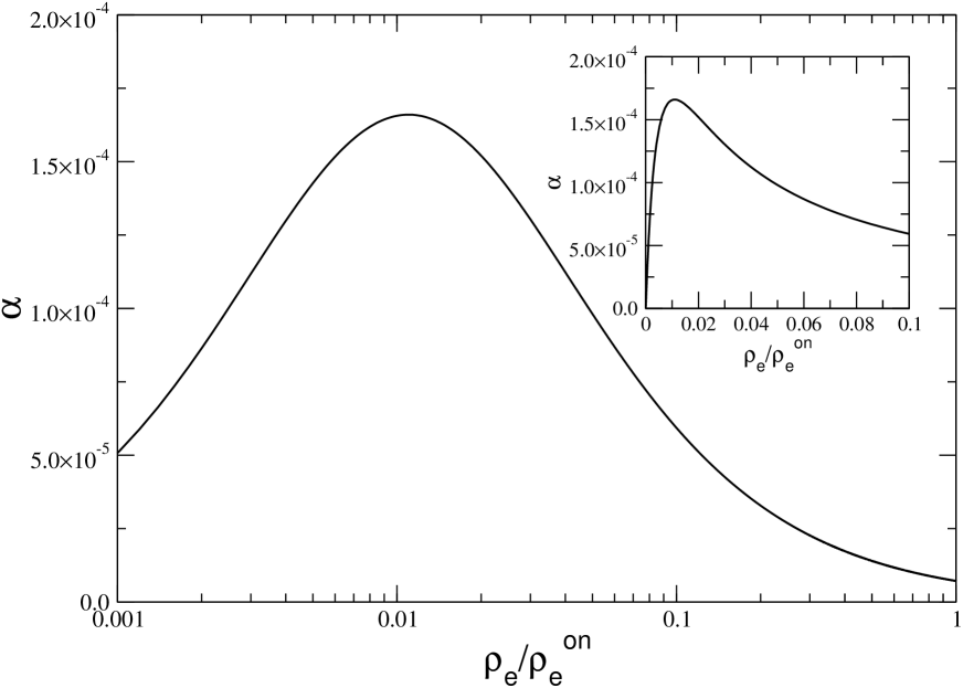
If we go away from the “on” state with the JoFET, we reduce both and linearily by depleting the density of states. Fig. 3 shows that we find that the dissipative effects are strongest during the switching process when , and not in the “on” state of the switch. In the “off” state of the switch (for ) also goes to zero. If the switch is tuned from the “off” state to the “on” state, reaches a local maximum and then decreases again. This makes the JoFET a very attractive switch: It induces an acceptably low level decoherence in the “on” state and can be made completely silent in the “off” state.
An SFS junction in the -state is based on a metallic material, thus the estimate of the shunt resistance in the RSJ model yields a much smaller result than in the case of the JoFET, sfs . The critical current of the SFS junction is mA. Thus, leaving the transformer properties unchanged, we find pH. Using these estimates the strength of the dissipative effects is of the order of . This makes such a device unsuitable at the present level of technology, however, it appears that SIFS junctions kontos are by far closer to the desired values, see Fig. 4.
High- junctions can be realized in different ways. Here, we take from Ref. hightc parameters for a typical noble metal (Au)-bridge junction with a film thickness of about nm. The product mV and nm. We assume that in principle for the -state and the 0-state are the same. For a contact area of around x nm2, mA and . Now the strength of the dissipative effects is easily evaluated to be , which is way better than SFS -junctions and even better than the JoFET.
We estimated the strength of the dissipative effects that will occur due to the switch for several possible switches. These results are summarized in figure 4 for typical parameters of the analyzed systems. We find that the noise properties of a JoFET and -shifters based on High-Tc-materials introduce no important noise source. On the other hand, the parameters found from -shifters based on magnetic materials are much less encouraging.
We would like to thank T.P. Orlando, P. Baars and A. Marx for useful discussions. Work supported by ARO through Contract-No. P-43385-PH-QC.
References
- (1) Yu. Makhlin, G. Schön, and A. Shnirman, Rev. Mod. Phys. 73, 357–400 (2001).
- (2) T.P. Orlando, J.E. Mooij, C.H. van der Wal, L. Levitov, S. Lloyd, J.J. Mazo, Phys. Rev. B 60, 15398 (1999); J.E. Mooij, T.P. Orlando, L. Levitov, L. Tian, C.H. van der Wal, S. Lloyd, Science 285, 1036 (1999).
- (3) C.H. van der Wal, A.C.J. ter Haar, F.K. Wilhelm, R.N. Schouten, C.J.P.M Harmans, T.P. Orlando, S. Lloyd, J.E. Mooij, Science 290, 773 (2000).
- (4) I. Chiorescu, Y. Nakamura, C.J.P.M. Harmans, and J.E. Mooij, Science 299, 1869 (2003).
- (5) C.H. van der Wal, F.K. Wilhelm, C.J.P.M. Harmans, and J.E. Mooij, Eur. Phys. J. B 31, 111 (2003).
- (6) X. Zhou, Z.-W. Zhou, G.-C. Guo, and M.J. Feldman, Phys. Rev. Lett 89, 197903 (2002)
- (7) A. Richter, Adv. Sol. St. Phys. Vol. 40, 321.
- (8) G. Blatter, V.B. Geshkenbein, L.B. Ioffe, Phys. Rev. B 63, 174511 (2001).
- (9) K.A. Delin and A.W. Kleinsasser, Supercond. Sci. Technol. 9, 227 (1996).
- (10) V.V. Ryazanov, V.A. Oboznov, A.Yu. Rusanov, A.V. Veretennikov, A.A. Golubov, and J. Aarts, Phys. Rev. Lett. 86, 2427 (2001).
- (11) M. Tinkham: Introduction to Superconductivity, 2nd ed., McGraw-Hill (1996).
- (12) M.J. Storcz and F.K. Wilhelm, Phys. Rev. A 67 042319 (2003).
- (13) B. Singh and T.P. Orlando, private communication.
- (14) I.O. Kulik and A.N. Omelyanchuk, Sov. J. Low Temp. Phys. 3, 459 (1977)
- (15) T. Kontos, M. Aprili, J. Lesueur, F. Genêt, B. Stephanidis, and R. Boursier, Phys. Rev. Lett. 89 137007 (2002).