The effect of electromechanical coupling on the strain in AlGaN/GaN heterojunction field effect transistors
Abstract
The strain in AlGaN/GaN heterojunction field-effect transistors (HFETs) is examined theoretically in the context of the fully-coupled equation of state for piezoelectric materials. Using a simple analytical model, it is shown that, in the absence of a two-dimensional electron gas (2DEG), the out-of-plane strain obtained without electromechanical coupling is in error by about 30% for an Al fraction of 0.3. This result has consequences for the calculation of quantities that depend directly on the strain tensor. These quantities include the eigenstates and electrostatic potential in AlGaN/GaN heterostructures. It is shown that for an HFET, the electromechanical coupling is screened by the 2DEG. Results for the electromechanical model, including the 2DEG, indicate that the standard (decoupled) strain model is a reasonable approximation for HFET calculataions. The analytical results are supported by a self-consistent Schrödinger-Poisson calculation that includes the fully-coupled equation of state together with the charge-balance equation.
pacs:
73.21.Ac, 71.20.Nr, 85.30.Tv, 73.20.At, 73.61.Ey, 77.65.LyI Introduction
The piezoelectric and spontaneous polarization properties of the AlxGa1-xN material system makes it attractive for certain wide bandgap device applications. Heterojunction field-effect transistors (HFETs) made from AlGaN/GaN possess two-dimensional electron gas (2DEG) concentrations on the order of at the AlGaN/GaN interface. Owing to the polarization effects, the 2DEG can be established at zero gate bias and achieved without intentional doping.[1, 2, 3, 4, 5, 6] A back doping design[7] can further increase the 2DEG concentration to approximately . The dense 2DEGs result in r.f. device power densities in the range 6 – 12 W/mm, making AlGaN/GaN HFETs attractive for high-power applications.
The formation of the 2DEG can be traced directly to the large built-in polarization fields in the material system. In addition to the piezoelectric polarization due to the strain induced by the lattice mismatch, there is a spontaneous polarization in the direction along the -axis which can be several times larger than the piezoelectric polarization. These polarizations induce local electric fields which, in turn, cause a notch to form in the conduction band edge at the interface. Electrons congregate in the notch, either from surface states or from unintentional dopants and traps, forming the 2DEG.
In previous HFET analyses, the electrical and mechanical properties of the epitaxial layers have been treated independently. The standard elastic theory is applied and Hooke’s law is assumed to hold in obtaining the strain tensors in each material layer. In effect, this assumption decouples the strain tensor from the Poisson and Schrödinger equations and renders the task of computing the free charge distribution and band structure more tractable. In reality, however, the electrical and mechanical properties of piezoelectric materials are coupled as seen from thermodynamics[8] and are best treated using a unified approach, especially since the piezoelectric response is large in AlGaN for high Al fractions.
In other work, large modifications to the elastic properties have been predicted for buried group III-nitride nanostructures[9] and free-standing plates of AlN.[10] The latter is a geometry closely related to the AlGaN barrier layer of the HFET. As a direct comparison, we take an AlN plate experiencing biaxial strain equivalent to the strain of a pseudomorphic AlN layer on GaN, or . The resulting strain using an uncoupled calculation in the absence of spontaneous polarization is and the electric field is MV/cm. In the coupled calculation, we obtain and MV/cm. Based on these substantial differences there is strong motivation to make a detailed analysis of a transistor structure including a detailed analysis of the spontaneous polarization moment and free carrier distributions.
In the present work, the strain and electric fields obtained from the fully-coupled model are contrasted with those from the standard model for a representative HFET structure. The deviations from the standard model are discussed in detail. The theory uses the fully-coupled piezoelectric equation of state to obtain the strain field. A simple analytical model is then used to obtain the interaction between the polarization-induced electric field and the strain tensor. Also included is the effect of 2DEG charge-screening on the electromechanical coupling. The results from the analytical model are supported by those from a self-consistent Schrödinger-Poisson model that includes charge balance and free hole states.
This paper is organized as follows: In Sec. II, the strain tensor is derived from the fully-coupled equation of state. The Poisson equation is solved analytically for a bi-layer AlGaN/GaN slab and the strain components and electric field in the barrier material is derived in closed form. In Sec. III, the calculated deviations of the standard model relative to the fully-coupled model are shown. The effect of screening from the 2DEG is discussed. The results from a fully-coupled numerical model are presented. The results are summarized in Sec. IV.
II Model description
The fully-coupled equation of state for piezoelectric materials is expressed as[11]
| (1) |
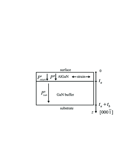
in component form where is the stress tensor, is the fourth-ranked elastic stiffness tensor, is the strain tensor, is the third-ranked piezoelectric coefficient tensor, is the electric field vector, and the indices , , , and run over the Cartesian coordinates , , and . Summation over repeated indices has been suppressed. Eq. (1) in the absence of piezoelectric coupling () is recognized as Hooke’s law relating stress to strain. The fully-coupled model is now applied to the representative HFET structure shown in Fig. 1. A one-dimensional (1-D) approach is used where the strain in the bi-layer slab is assumed to be piecewise homogeneous. This approximation means that is diagonal for the coordinates defined in Fig. 1 and that and are, to first order, uniform in each layer. The strain induces a piezoelectric polarization given by
| (2) |
From straightforward electrostatics we know that Eqs. (1) and (2) are coupled through the Poisson equation which is written in our notation as
| (3) |
where is the electrostatic potential, is the electric permittivity, is the charge distribution and includes both ionic and free charges, is the spontaneous polarization, and has been defined in Eq. (2). In the absence of shear strains, and are directed in the direction for a cation-faced structure as shown in Fig. 1, and with the sixfold rotational symmetry along the -axis, . From Eq. (2), the piezoelectric polarization along for wurtzite materials then becomes
| (4) |
It is assumed that is determined by the atomic alignment in the -plane across the AlGaN/GaN interface. This pseudomorphic boundary condition gives
| (5) |
in the AlGaN layer and in the GaN layer, where and are the -plane lattice constants in the AlGaN and GaN layers, respectively. In reality, besides the force exerted on the AlGaN layer by the GaN layer, one would also expect the AlGaN layer to exert a force on the GaN layer, causing some strain on the GaN side of the interface. This local distortion of the lattice would be a maximum at the junction and become vanishingly small towards the interior of the GaN. Such refinements, however, would require a three-dimensional (3-D) modeling of the electromechanical problem, as it would have to include non-zero and position-dependent shear terms in the strain tensor. This is beyond the scope of the present work and is not essential for our investigation.
Thus, within the present work, is assumed to be decoupled from the electrical properties, essentially fixed by the bonding arrangement at the interfacial plane, with serving as the principal vehicle for electromechanical coupling. From Eq. (1) and from the foregoing assumptions, the normal component of the stress tensor is given by
| (6) |
From the boundary conditions for a free surface, the stresses along the outward normal must be zero. As a consequence, Eq. (6) then gives for the 1-D case
| (7) |
which is the out-of-plane strain, where . From Eq. (7), it is seen that the first term is consistent with the Poisson ratio of the standard model for and a new coupled term representing the electromechanical coupling. To date, the latter has not been included in AlGaN/GaN HFET models. The extent of the coupling will depend on the Al mole fraction and the electric field in the layers, which, in turn, will depend on the charge distribution and boundary conditions used to solve Eq. (3). The actual problem is quite complicated and involves the self-consistent solution of the equation of state in conjunction with the Poisson, Schrödinger, and charge balance equations. To illustrate the concept of electromechanical coupling without obscuring much of the underlying physics, a simple example has been contrived from which analytical results can be extracted so that the effect of coupling can be easily quantified. The charges assumed herein are the polarization space charges and a sheet electron distribution at the AlGaN/GaN interface. Ordinarily, the electron distribution should be calculated quantum-mechanically from the electron eigenstates, as described in Ref. [12]. In order to illustrate these effects analytically, the 2DEG is modeled here as a function localized at the AlGaN/GaN interface. These induced electrons may be accounted for by surface charges such as donor states, by deep-level traps in the AlGaN and GaN layers, or by unintentional dopants. The exact origin of the induced 2DEG is still unknown, but its presence is well-established from previous work.[1] As will be seen later, representative values for the induced 2DEG are used. The 1-D Poisson equation then becomes
| (8) | |||
| (9) |
where is the areal 2DEG concentration and is the magnitude of the electronic charge. Equation (8) is integrated to obtain subject to the boundary conditions at and and also to the continuity of and the electric displacement across the interface. The condition at the two surfaces presumes that the polarization charge of the materials is terminated by external charges and that the applied bias voltage is zero. The general solution in each layer, obtained by integrating Eq. (8) twice, is given by
| (10) |
where
| (11) |
and is layer-dependent because of the varying elastic and piezoelectric coefficients, and and are unknown constants. Thus there are four unknowns, two in each layer. The ’s are eliminated by enforcing the boundary conditions at and . It should also be noted that in the GaN buffer because of the simplifying assumptions made previously. The relationship between the two ’s is established from the continuity of the electric displacement and is found by integrating Eq. (8) across the AlGaN/GaN interface (see Fig. 1) encompassing the 2DEG. This boundary condition gives the relation between the electric fields in the two layers as
| (12) |
From Eq. (12), we obtain the relation between the ’s in the respective layers as
| (13) |
From Eq. (13) and from the continuity of across the interface, we can solve for all of the remaining unknowns.
The results are greatly simplified in the limit , a condition that is met for most HFETs. In this limit, the electrostatic potential in the AlGaN layer is given by
| (14) | |||
| (15) |
and is constant in the GaN layer. From Eq. (14), the electric field in the AlGaN layer is given by
| (16) | |||
| (17) |
The electric field within the standard model is obtained by replacing with in Eq. (16). It is seen that for growth along , the electric field in the AlGaN from the coupled model is smaller that of the standard model, since is always positive. The vertical strain component within the fully-coupled model is obtained from
| (18) | |||
| (19) |
The first term in Eq. (18) is the typical result obtained from uncoupled elastic theory. The remaining terms are due to electromechanical coupling.
Besides the simple analytical approach described in this work, a previously-published numerical Schrödinger-Poisson model[12, 13] has been modified to include full coupling. The elements of the strain tensor enter the Schrödinger equation via deformation potential theory. One of these elements, , is now a function of the electrostatic potential calculated from the Poisson equation. In turn, the electrostatic potential is a function of the piezoelectric polarization, itself a function of . With each Schrödinger-Poisson iteration, the strain must be updated via Eq. (7). Also included is the charge-balance equation as described in Ref. [12]. The calculation is regarded as having converged when the maximum change in the electrostatic potential between the current and the previous iteration is less than 0.01 meV.
III Results and discussion
This section contains calculations used to compare the uncoupled and coupled models for a model HFET structure. The presence of the 2DEG and its effect on the problem are investigated. Table I shows the material parameters[14, 15, 16, 17, 18, 19, 20] used in the calculations. The signs of the polarization parameters are defined in relation to the [0001] direction: a negative sign means that the vector is in the direction.
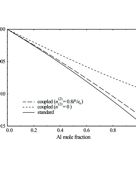
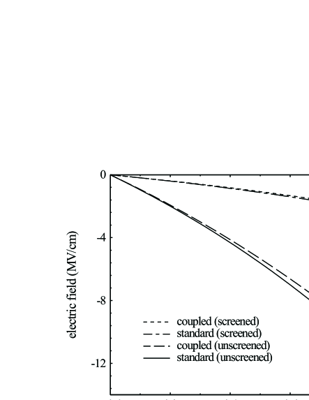
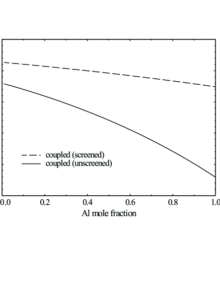
The calculated strain for both the standard and fully-coupled models as a function of the Al fraction of the barrier layer is shown in Fig. 2. It is seen that the electromechanical coupling changes significantly in the absence of a 2DEG. It is also noted that the coupling reduces relative to the standard model. This result is evident from Eq. (7) in which it is seen that the coupling opposes the contraction of material along the axis when there is tensile strain in the plane. A realistic comparison between the two approaches should include the mobile charge drawn to the interface by the polarization space charge. The net polarization space charge at the interface is given by , and for a 30% Al alloy composition is approximately . The 2DEG can be expected to neutralize the space charge to some extent. In Fig. 2, is taken to be , although it will be seen shortly from a Schrödinger-Poisson solution that the neutrality factor is closer to 0.9. With screening from the 2DEG included, the discrepancy between the two models is reduced. This result is due to the reduction in the polarization-induced electric field caused by screening and is shown more clearly in Fig. 3. The magnitude of the 2DEG chosen here is representative of the induced electrons seen in actual HFET devices.[1] We do not, however, explore the origin of the 2DEG in this simple approach, as the only purpose in including the 2DEG is to show that electron screening has a strong influence on the electromechanical coupling.
Next we examine the deviation between the coupled and uncoupled models. The deviation in the out-of-plane strain component is defined as
| (20) |
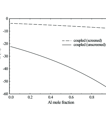
where is given by Eq. (18) for both the screened and unscreened cases. The calculated is shown in Fig. 4. For a typical HFET with an Al mole fraction of 0.3, the error is about 30% if the effect of the 2DEG is neglected, as compared to 17% for free-standing plates of AlN. It is clear that if the AlGaN layer is considered in isolation, the standard model gives a large error in the strain tensor. In an HFET structure, however, the importance of the AlGaN/GaN interface cannot be overestimated. This interface introduces additional physics, the most important being the 2DEG. Effectively, the presence of a large 2DEG restores the validity of the standard model.
Fig. 5 shows the difference in when the spontaneous polarization is excluded. It is well-known that the spontaneous polarization is the larger of the two polarizations in the AlGaN/GaN material system. For example, for a Al fraction of 0.3, the space charge induced by the discontinuity of the spontaneous polarization is about as compared to about for the piezoelectric polarization. The difference increases for higher Al fractions. Accordingly, with just the piezoelectric polarization included, the electromechanical coupling is underestimated. This is because the electric field is reduced compared to Fig. 3. Once again, however, the screening from the 2DEG reduces the coupling.
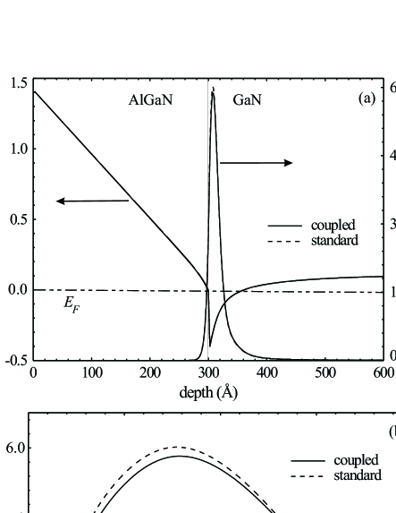
Fig. 6(a) shows the conduction band edge and the free electron distribution obtained from the Schrödinger-Poisson calculation that includes the full electromechanical coupling. The structure is a standard HFET design consisting of 300 Å of N on a thick GaN buffer. The 2DEG is assumed to come from surface donor states[12] having an activation energy of 1.4 eV below the conduction band edge at the surface, effectively pinning the surface potential at 1.4 V. The resulting 2DEG concentration after convergence is about . This magnitude is about , almost neutralizing the polarization-induced space charge. As an example, the electric field in the N layer in the absence of a 2DEG is about 3.1 MV/cm from Fig. 3. The fully-coupled Schrödinger-Poisson model gives a field of about 0.45 MV/cm and the standard Schrödinger-Poisson model a field of about 0.46 MV/cm. Within numerical errors, the 2DEG is almost unchanged between the coupled and standard models as shown more clearly in Fig. 6(b). Consequently, there is little change in the conduction band edge between the two models. The calculated eigenstates from the Schrödinger equation and the electrostatic potential from the Poisson equation show little change relative to the standard model after both models have converged to a solution.
IV Summary and conclusions
In summary, a fully-coupled electromechanical model has been presented for the strain in AlGaN/GaN HFETs. The model goes beyond the standard Hooke’s law description and uses the fully-coupled equation of state for the stress-strain relationship. Using a simple analytical model for the HFET, it is shown that the present model gives rise to significant changes in the strain field and, consequently, to the electronic properties of the device in relation to the standard model in the absence of free charges. When free charges are present in the form of a 2DEG, the built-in electric field is reduced through the screening of the fixed space charge. This effect, in turn, reduces the electromechanical coupling and brings the results from the standard and fully-coupled models into closer agreement.
Acknowledgements.
The work of BJ was partially supported by the Air Force Office of Scientific Research (AFOSR) and performed at Air Force Research Laboratory, Materials and Manufacturing Directorate (AFRL/MLP), Wright Patterson Air Force Base under USAF Contract No. F33615-00-C-5402.REFERENCES
- [1] O. Ambacher, B. Foutz, J. Smart, J. R. Shealy, N. G. Weimann, K. Chu, M. Murphy, A. J. Sierakowski, W. J. Schaff, L. F. Eastman, R. Dimitrov, A. Mitchell, and M. Stutzmann, J. Appl. Phys. 87, 334 (2000).
- [2] J. Antoszewski, M. Gracey, J. M. Dell, L. Faraone, T. A. Fisher, G. Parish, Y.-F. Wu, and U. K. Mishra, J. Appl. Phys. 87, 3900 (2000).
- [3] Y. Zhang, I. P. Smorchkova, C. R. Elsass, S. Keller, J. P. Ibbetson, S. Denbaars, U. K. Mishra, and J. Singh, J. Appl. Phys. 87, 7981 (2000).
- [4] J. P. Ibbetson, P. T. Fini, S. P. DenBaars, J. S. Speck, and U. K. Mishra, Appl. Phys. Lett. 77, 250 (2000).
- [5] S. L. Rumyantsev, N. Pala, M. S. Shur, R. Gaska, M. E. Levinshtein, M. A. Khan, G. Simin, X. Hu, and J. Yang, J. Appl. Phys. 88, 6726 (2000).
- [6] C. P. Jiang, S. L. Guo, Z. M. Huang, J. Yu, Y. S. Gui, G. Z. Zheng, J. H. Chu, Z. W. Zheng, B. Shen, and Y. D. Zheng, Appl. Phys. Lett. 79, 374 (2001).
- [7] N. Maeda, K. Tsubaki, T. Saitoh, T. Tawara, and N. Kobayashi, Mat. Res. Symp. Proc. 743, L9.3.1 (2003).
- [8] J. F. Nye, Physical Properties of Crystals – Their representation by Tensors and Matrices (Clarendon Press, Oxford, 1985), p. 179.
- [9] E. Pan, J. Appl. Phys. 91, 3785 (2002).
- [10] E. Pan and B. Yang, Proc. of the 4th Int. Conference Nonlinear Mech., Shanghai, pp. 479-484 (2002).
- [11] J. Zelenka, Piezoelectric Resonators and their Applications (Elsevier, Amsterdam, 1986), Vol. 24, p. 33.
- [12] B. Jogai, J. Appl. Phys. 91, 3721 (2002).
- [13] B. Jogai, Phys. Stat. Sol. (b) 233, 506 (2002).
- [14] A. F. Wright, J. Appl. Phys. 82, 2833 (1997).
- [15] W. M. Yim, E. J. Stofko, P. J. Zanzucchi, J. I. Pankove, and M. Ettenberg, J. Appl. Phys. 44, 292 (1973).
- [16] H. P. Maruska and J. J. Tietjen, Appl. Phys. Lett. 15, 327 (1969).
- [17] K Tsubouchi, K. Sugai, and N. Mikoshiba, IEEE Ultrason. Symp. 1, 375 (1981).
- [18] M. S. Shur, A. D. Bykhovski, and R. Gaska, MRS Internet J. Nitride Semicond. Res. 4S1, G1.6 (1999).
- [19] F. Bernardini, V. Fiorentini, and D. Vanderbilt, Phys. Rev. B 56, R10024 (1997).
- [20] V. W. L. Chin, T. L. Tansley, and T. Osotchan, J. Appl. Phys. 75, 7365 (1994).
| Material | (Å) | ||||||
|---|---|---|---|---|---|---|---|
| AlN | 108a | 373a | 3.112b | 0.58d | 1.55d | 0.081f | 8.5g |
| GaN | 103a | 405a | 3.189c | 0.36e | 1e | 0.029f | 10g |
