Effect of Impurities in the Channel of a Spin Field Effect Transistor (SPINFET)
Abstract
We show that the conductance of Spin Field Effect Transistors (SPINFET) [Datta and Das, Appl. Phys. Lett., 56, 665 (1990)] is affected by a single (non-magnetic) impurity in the transistor’s channel. The extreme sensitivity of the amplitude and phase of the transistor’s conductance oscillations to the location of a single impurity in the channel is reminiscent of the phenomenon of universal conductance fluctuations in mesoscopic samples and is extremely problematic as far as device implementation is concerned.
1 Introduction
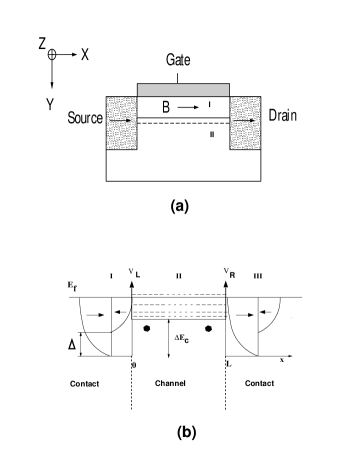
In a seminal paper published in 1990, Datta and Das [1] proposed a gate controlled electron spin interferometer which is an analog of the standard electro-optic light modulator. Their device (later dubbed ”Spin Field Effect Transistor” or SPINFET) consists of a one-dimensional semiconductor channel with ferromagnetic source and drain contacts (Fig. 1(a)). Electrons are injected into the channel from the ferromagnetic source with a definite spin orientation, which is then controllably precessed in the channel with a gate-controlled Rashba interaction [2], and finally sensed at the drain. At the drain end, the electron’s transmission probability depends on the relative alignment of its spin with the drain’s (fixed) magnetization. By controlling the angle of spin precession in the channel with a gate voltage, one can modulate the relative spin alignment at the drain end, and hence control the source-to-drain current (or conductance). This is the principle of the SPINFET.
There have been some studies of spin transport in such a device. Mireles and Kirczenow [3, 4] carried out a study of ballistic spin transport, but they overlooked two crucial features that are always present in a real device structure. First, there is an axial magnetic field along the channel caused by the ferromagnetic source and drain contacts which are magnetized in the same direction. This field can be quite strong ( 1 Tesla) [5] and dramatically alters the dispersion relations of the subbands in the channel, causes spin mixing, and has a serious effect on spin transport. Second, there will always be a few impurities in the channel (even if they are remote impurities) associated with channel doping or unintentional defects. We show that even a single (non-magnetic) impurity can cause spin relaxation in the presence of the axial magnetic field.
2 Theoretical Approach
We first consider the quasi one-dimensional semiconductor channel of a SPINFET in the absence of any impurities. The channel is along the x-axis (Fig. 1(a)) and the gate electric field is applied along the y-direction to induce a Rashba spin-orbit coupling in the channel. This system is described by the single particle effective-mass Hamiltonian [6]
| (1) |
where is the unit vector along the y-direction in Fig. 1(a) and is the vector potential due to the axial magnetic field along the channel (x-direction) caused by the ferromagnetic contacts. In (1), is the Bohr magneton ( ) and is the effective Landé g-factor of the electron in the channel. The quantity is the Rashba spin-orbit coupling strength which can be varied with the gate potential. The confining potentials along the y- and z-directions are denoted by and , with the latter being parabolic in space.
In (1), represents an interfacial potential barrier between the ferromagnetic contacts and the semiconducting channel. If the contact neighborhood consists of heavily doped semiconductor material in close proximity to a metallic ferromagnet, the Schottky barriers at the interface will be very narrow and electrons from the contacts can tunnel fairly easily into semiconducting channel resulting in a nearly-ohmic contact. We model these ultra-narrow Schottky barriers as delta-barriers given by:
| (2) |
where and are assumed equal ( = = ). In practice, the strength of the barrier depends on the ferromagnetic materials and also on the doping level in the channel. These barriers have a beneficial effect; they can facilitate coherent spin injection across a metallic ferromagnet and a semiconducting paramagnet interface [7, 8] which is crucial for the SPINFET.
In (1), we have neglected a few effects for the sake of simplicity. We have neglected the normal Elliott-Yafet interaction [9] because it is weak in quasi one-dimensional structures (where elastic scattering is strongly suppressed). We have also neglected the Dresselhaus interaction [10] since it does not relax spin when the initial spin polarization is along the axis of the wire [11, 12]. The Dresselhaus interaction can however be easily included in the Hamiltonian and is left for future work.
The choice of the Landau gauge = (0, -Bz, 0) allows us to decouple the y-component of the Hamiltonian in (1) from the x-z component. Furthermore, in the absence of any impurity scattering potential (), the Hamiltonian in the semiconducting channel is translationally invariant in the x-direction and the wavevector is a good quantum number. The eigenstates of the system can then be determined using plane waves traveling in the x-direction [13]. The two-dimensional Hamiltonian in the plane of the channel (x-z plane) is therefore given by
| (3) | |||||
where is the curvature of the confining potential in the z-direction, , and is the potential barrier between the ferromagnet and semiconductor. We assume that includes the effects of the quantum confinement in the y-direction (Fig.1(a)).
To model localized non-magnetic impurities (i.e., which do not by themselves flip the spin) we use a standard model of delta-scatterers
| (4) |
for an impurity located at a distance from the left ferromagnet/semiconductor interface with scattering strength (assumed to be spin independent). In our numerical examples, we consider the case of both attractive ( negative) and repulsive ( positive) impurities. While (1) and (3) represent a ballistic channel with no scattering, addition of the scattering potential in (4) to (1) or (3) will result in a Hamiltonian describing a weakly disordered channel in which impurity scattering takes place. The eigenstates of this (spin-dependent) Hamiltonian can then be found using a transfer matrix technique to extract the electron wavefunction. From this wavefunction, we can calculate the (spin-dependent) transmission probability through the channel and ultimately the (spin-dependent) channel conductance. The details of the calculations have been presented elsewhere [13]. The linear response conductance of the spin interferometer (for injection from either the +x or -x polarized bands in the left contact) is found from the Landauer formula.
We model the ferromagnetic contacts by the Stoner-Wohlfarth model (Fig.1.(b)). The +x-polarized spin (majority carrier) and -x-polarized spin (minority carrier) band bottoms are offset by an exchange splitting energy . The solutions of the Schrödinger equation for injection from minority and majority spins from the left magnetic contact then be written throughout the entire device leading to the corresponding transmission probabilities and the conductance of the interferometer based on the Landauer formula (see [13]). The strength of the barrier at the ferromagnet/semiconductor interface is characterized by the following parameter
| (5) |
Typical values of vary in the range of 0 to 2 [14]. Using and = 1.05x cm-1, we get a barrier strength = 16 eV for Z = 2.
3 Numerical Examples
We consider a spin interferometer consisting of a quasi one-dimensional InAs channel between two ferromagnetic contacts. The electrostatic potential in the z-direction is assumed to be harmonic (with = 10 meV in (3). A Zeeman splitting energy of 0.34 meV is used in the semiconductor channel assuming a magnetic field B = 1 Tesla along the channel. This corresponds to a factor of 3 and an electron effective mass which is typical of InAs-based channels [1]. The Fermi level and the exchange splitting energy in the ferromagnetic contacts are set equal to 4.2 and 3.46 eV, respectively [15].
The Rashba spin-orbit coupling strength is typically derived from low-temperature magnetoresistance measurements (Shubnikov-de Haas oscillations) in 2DEG created at the interface of semiconductor heterostructures [16]. To date, the largest reported experimental values of the Rashba spin-orbit coupling strength has been found in InAs-based semiconductor heterojunctions. For a normal HEMT heterojunction, Sato et al. have reported variation of from 30- to 15 eV-m when the external gate voltage is swept from 0 to -6 V (the total electron concentration in the 2DEG is found to be reduced from 5- to 4.5 over the same range of bias).
Tuning the gate voltage varies both the potential energy barrier and the Rashba spin-orbit coupling strength . Both of these variations lead to distinct types of conductance oscillations. The variation of causes the Fermi-level in the channel to sweep through the resonant energies in the channel, causing the conductance to oscillate. These are known as Ramsauer oscillations and have been examined by us in detail in [13]. The variation of , on the other hand, causes spin precession in the channel leading to the type of conductance oscillation which is the basis of the spin interferometer, as originally visualized by Datta and Das [1]. In [13] we found that the Ramsauer oscillations are much stronger and can mask the oscillations due to spin precession, unless the structure is designed with particular care to eliminate (or reduce) the Ramsauer oscillations.
In the numerical examples below, we assumed that the Rashba spin-orbit coupling strength is constant (i.e., independent of the gate potential) and equal to the maximum reported value of 30 eV-m (best case scenario). We also used a value of Z = 0.25 corresponding to a value of and in (2) equal to 2 eV-. The scattering strength of the single impurity in the channel was set equal to = 0.25 eV- (the plus and minus sign corresponding to repulsive and attractive impurity, respectively).
First, we consider the case of a single repulsive scatterer (impurity) whose location is varied from the left to the rigth side of the channel in steps of 10 . Figure 2 shows that variation of the conductance with the impurity location for three different values of in the channel, i.e, gate potential on the SPINFET. It is seen that the condutance of the interferometer is a strong function of the impurity location. Figure 2 shows that the condutance modulation (difference between maximum and minimum conductance values) of the interferometer is about 0.9, 0.21, and 0.2 , for equal to 4.191, 4.188, and 4.185 eV, respectively. The same calculation were repeated for the case of an attractive impurity with the same magnitude of the scattering strength and the conductance modulation as a function of the impurity location are shown in Fig.3. In this case, the condutance modulation (difference between maximum and minimum conductance values) of the interferometer is about 0.76, 0.16, and 0.17, for equal to 4.191, 4.188, and 4.185 eV, respectively.
4 Conclusions:
In this paper, we have shown how the conductance of gate controlled spin interferometers proposed in [1] is strongly dependent on the location of a single impurity in the semiconducting channel (Figs. 2 and 3). The extreme sensitivity of the amplitude and phase of conductance oscillations of a SPINFET to impurity location is reminiscent of the phenomenon of universal conductance fluctuations of mesoscopic samples [17]. This will hinder practical applications of electron spin interferometers since it will lead to such problems as large threshold variability, random device characteristics, and general irreproducibility.
The work of S. B. was supported by the National Science Foundation.
References
- [1] S. Datta and B. Das, Appl. Phys. Lett., 56, 665 (1990).
- [2] E. I. Rashba, Sov. Phys. Semicond., 2, 1109 (1960); Y. A. Bychkov and E. I. Rashba, J. Phys. C, 17, 6039 (1984).
- [3] F. Mireles and G. Kirzcenow, Phys. Rev. B, 64, 024426 (2001).
- [4] F. Mireles and G. Kirzcenow, preprint cond-mat/0210391 at www.arxiv.org (2002).
- [5] J. Wróbel, T. Dietl, K. Fronc, A. Lusakowski, M. Czeczott, G. Grabecki, R. Hey and K. H. Ploog, Physica E, 10, 91-96 (2001).
- [6] A.V. Moroz and C.H.W.Barnes, Phys. Rev. B, 60, 14272 (1999); Phys. Rev. B 61, R2464 (2000).
- [7] E. I. Rashba, Phys. Rev. B, 62, 16267 (2000).
- [8] H.B. Heersche, Th. Schapers, J. Nitta, and H. Takayanagi, Phys. Rev. B, 64, 161307 (2001).
- [9] R. J. Elliott, Phys. Rev., 96, 266 (1954).
- [10] G. Dresselhaus, Phys. Rev., 100, 580 (1955).
- [11] A. Bournel, V. Delmouly, P. Dollfus, G. Tremblay and P. Hesto, Physica E, 10, 86 (2001); A. Bournel, P. Dollfus, P. Bruno and P. Hesto, Eur. Phys. J, AP 4, 1 (1998).
- [12] S. Pramanik, S. Bandyopadhyay and M. Cahay, Phys.Rev.B (in press).
- [13] M. Cahay and S. Bandyopadhyay, preprints cond-mat/0301052 and cond-mat/0305622 at www.arxiv.org (2003). Also, Phys. Rev. B (in press).
- [14] Th. Schäpers, G. Engels, J. Lange, Th. Klocke, M. Hollfelder, and H. Luth, J. Appl. Phys., 83, 4324 (1998).
- [15] We use the same values as in F. Mireles and G. Kirczenow, Europhys. Lett., 59, 107 (2002).
- [16] J. Nitta, T. Akazaki, H. Takayanagi, and T. Enoki, Phys. Rev. Lett., 78, 1335 (1997); Th. Schäpers, J. Nitta, H.B. Heersche, and H. Takayanagi, Phys. Rev. B, 64, 125314 (2001); Y. Sato, T. Kita, S. Gozu and S. Yamada, J. Appl. Phys., 89, 8017 (2001); Y. Sato, S. Gozu, T. Kita and S. Yamada, Physica E, 12, 399 (2002).
- [17] S.C. Feng, P.A. Lee and A.D. Stone, Phys. Rev. Lett. 56, 1960 (1986); P.A.Lee, A.D.Stone, and H.Fukuyama, Phys. Rev. B.35, 1039 (1987).

