Control of Coulomb blockade in a mesoscopic Josephson junction using single electron tunneling
Abstract
We study a circuit where a mesoscopic Josephson junction (JJ) is embedded in an environment consisting of a large bias resistor and a normal metal - superconductor tunnel junction (NIS). The effective Coulomb blockade of the JJ can be controlled by the tunneling current through the NIS junction leading to transistor-like characteristics. We show using phase correlation theory and numerical simulations that substantial current gain with low current noise ( fA/) and noise temperature ( 0.1 K) can be achieved. Good agreement between our numerical simulations and experimental results is obtained.
pacs:
74.78.Na, 85.25.Am, 85.35.GvMesoscopic Josephson junctions (JJ) display interesting phenomena owing to the conjugate nature of phase and charge Tinkham . Coulomb effects cause delocalization of the macroscopic phase variable across the tunnel junction, which leads to the formation of energy bands ALZ . As the band width grows rapidly with the band index, a mesoscopic JJ makes it possible to construct novel devices where the operation is based on controlling the transitions between energy levels of the junction, thereby controlling the effective Coulomb blockade of the device sep1 ; has1 . The control is made using a small tunnel current of single electrons. Thus, the device distinguishes from the ordinary Coulomb blockade devices, like single electron transistors (SETs), where the current is adjusted by an external, capacitively-coupled voltage review .
We have investigated the circuit where a mesoscopic Josephson junction (JJ) is embedded in an environment consisting of a large bias resistor and a normal metal - superconductor tunnel junction (NIS). The JJ is biased in the regime where the system becomes a two-level system with two distinct Coulomb blockade strengths. The effective Coulomb blockade of the JJ is controlled by the tunneling current through the NIS junction, which leads to transistor-like characteristics. This device, called the Bloch oscillating transistor (BOT) has1 , provides a low-noise current amplifier whose input impedance level makes it an intermediate device between the ultimate low temperature amplifiers, the SQUID and the SET science .
In this Article, we present experimental results on the basic properties of BOTs, and compare them with computer simulations based on time dependent phase correlation theory for electron and Cooper pair tunneling. We show that this provides a way to model the devices quantitatively. Noise properties of the devices are discussed, the conclusion being that ultra low-noise current amplifiers (current noise fA/ referred to input) can be built on the basis of controlled JJs. The simulated results are shown to be in a good agreement with our experimental findings.
Schematically our device is shown in Fig. 1 (left frame). A Josephson junction (JJ) connects a superconducting island to the emitter electrode (E). A Normal-Insulator-Superconductor (NIS) junction connects the normal base electrode (B) to the island. Furthermore, a high-impedance, thin film resistor connects the island to the collector electrode (C). When the isolation resistance , charge fluctuations on the JJ are small and the dynamics of the junction consists purely of Bloch reflections at the Brillouin zone boundary, interrupted by occasional Zener tunneling between the bands Zener .
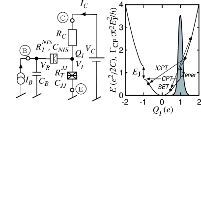
Fundamentally, the operation of a BOT is understood on the basis of the band structure of a Josephson junction. The energy versus (quasi)charge of a JJ is shown with a thick uniform curve in the right frame of Fig. 1. When the collector is voltage biased by , the ”island” charge tends to relax through towards the value , where . At , Cooper pair (CP) tunneling returns the system back to the state . Repetition of this Bloch oscillation cycle produces a net current from the collector to the emitter. The competing process for the CP tunneling at is Zener tunneling up to the second energy band, where Bloch oscillations do not occur and the current flow stops (Coulomb blockade voltage ). From the second band the system may return back to the first one by single-electron tunneling through the base junction. Thus, as a result of a single electron tunneling event through the NIS junction, a sequence of Cooper pair pulses is injected through the JJ, which leads to a current gain equaling the average number of electrons in the CP sequence. This kind of action is below referred to as regular BOT operation.
The above picture is, however, an overidealization in most experimental cases. In a real situation all input electrons do not produce output current pulses, but rather cause intraband transitions. It is also hard to fabricate large enough thin film resistances to achieve coherent Bloch oscillations. Qualitatively, the picture of the two-level system still works, but the measured current gains are clearly less than the calculated values PhysicaE . When becomes relatively small, , charge fluctuations grow and inelastic Cooper pair tunneling may take place clearly before the Brillouin zone boundary. This makes the dynamics more complicated and our present experiments and simulations are aimed at clarifying this question.
| (fF) | (fF) | / | ||||
|---|---|---|---|---|---|---|
| 1 | 8.1 | 27.3 | 23 | 0.28 | 0.95 | 22 / 78 |
| 2 | 7.8 | 5.8 | 50 | 0.6 | 1.0 | 83 / 83 |
In our computational model the island charge as function of time is obtained by integrating the equation
| (1) |
where the first term represents the charge relaxation through the collector resistor, and the last two terms represent tunneling current in the NIS and JJ, respectively. contains only quasiparticle current while includes both quasiparticle and Cooper pair tunneling. The base junction is current biased, as in the experiments, but the gate capacitance pF (see Fig. 1) converts it effectively into voltage bias NOTE .
To integrate Eq. (1) in the presence of finite Josephson coupling and electromagnetic environment, we compute the Cooper pair tunneling through the JJ () and quasiparticle tunneling through both junctions (, ) using the phase-fluctuation -theory dev1 ; ing1 . As a modification to the standard theory, we use time dependent voltages and across the JJ and NIS junctions, respectively. is given by
| (2) |
A basically similar modelling approach has been employed by Kuzmin et al. Kuzmin96 when investigating the role of Zener tunneling on the IV-curves of ultra small Josephson junctions. The difference is that we include the effect of quantum fluctuations in our model on top of the thermal noise which was employed in Ref. Zaikin92 only.
According to the -theory, tunneling does not happen strictly at , but is rather represented with a finite distribution, which is schematically shown in Fig. 1. Within this picture, one can still use the concept of band structure, the interpretation being that values correspond to the first band, and to the second band. The band gaps, where Zener tunneling takes place, are now reflected in the probabilities at which the junction may pass from the lower to the higher band (see below).
The most critical assumption is made while computing the Cooper pair tunneling rate, for which the lowest order theory is valid when ing1 . For the samples analyzed in this paper, and , so that second order effects may be expected to be small. The Cooper pair tunneling rate can then be computed as
| (3) |
where the function is defined as
| (4) |
The phase correlation function which takes into account the fluctuations of the phase on the junction. is calculable from the real part of the environmental impedance ing1 . Here we have also made the assumption that the effect of the environment is exclusively due to the collector resistance note , for which the function was calculated numerically.
In the limit , the CP tunneling rate as given by Eq. 3 becomes a Gaussian distribution centered around ing1 . If furthermore , the distribution narrows to a delta spike which equals the equation obtained from the band model by neglecting the effect of the environment sch1 . Hence, the basic features of the band model are embedded in the peaked tunneling probabilities. In a proper band model, however, the capacitance of the JJ entering Eq. (1) would be nonlinear and given by . In our model, we take the capacitance as constant, which is valid in the limit only.
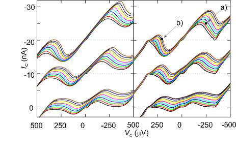
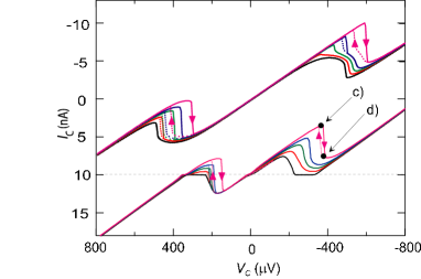
Our sample parameters are given in Table I. Details of sample manufacturing and experimental techniques can be found in Ref. science . Measured and computed -curves for sample I with various are shown in Fig. 2, each at several values of . When , a weak Coulomb blockade is visible at zero bias. The peak in current at non-zero voltages reflects Cooper pair tunneling processes, which are enhanced by single-electron current through the base. The current gain is found to be maximized in the region with negative slope: at ( nA) and at ( nA). From our simulations we get ( nA) and 2.5 ( nA), respectively. The relatively small maximum gains are caused by large current fluctuations owing to k. Fig. 3 displays -curves for sample II with . Both the measured data science and the simulated -curves display hysteretic behavior. The computed curves in the regular BOT regime are seen to display growing hysteresis with increasing base current, in accordance with the measured data. Especially with large , the current peak is at slightly lower voltages in the computed curves than in the measured data indicating that the computed probability of Zener tunneling is larger than in reality. This is a sign that our simplified picture of the energy band structure fails for large .
The nonsymmetrical nature of the curves in Fig. 2 suggests that the mechanism for current gain is different at opposite biasing polarities. This is illustrated in the time traces of in Figs. 4a and 4b. In the regular biasing case (, Fig. 4a) single-electron tunneling is seen to drive the system downwards from the upper band and, thus, it tries to restore Bloch oscillations, i.e. the dynamics is essentially similar to the original BOT operation even though incoherent tunneling phenomena modifies it strongly. When , on the contrary, tends to drive the system into the second band, which leads to a suppression of 2e-oscillations as seen in Fig. 4b. The recovery of 2e-oscillations now takes place through incoherent 2e-tunneling, the tunneling probability of which is determined by the ”tail” of -function.
Time domain plots of for the two hysteretic -branches (see Fig. 3) are shown in Figs. 4c and 4d. On the upper branch (Fig. 4c) the dynamics is again regular BOT dynamics, essentially similar to that of Fig. 4a. Now it is obvious that the system almost never relaxes to its stationary state, since the inverse of -time constant is small compared to the tunneling rate . Single electron tunneling still clearly enhances Cooper pair tunneling. At the lower branch, the system seldom returns to the lowest band, and the base current mostly consists of tunneling events causing intraband transitions only. Therefore, Cooper pair tunneling is less likely and the collector current remains small. Two stable solutions can coexist since . Now, due to the current biased base electrode, and can each dynamically assume two different average values, while their difference remains the same leading to equal base currents in both cases.

In our simulations, the transition from non–hysteretic to hysteretic behavior can be crossed by increasing . This is because increasing enhances the stability of the type of solution presented in Fig. 4(c) by increasing the rate according to Eq. (3). Near the hysteresis point, the ratio of base tunneling currents, , made of contributions causing either interband transitions () or intraband transitions () is found to vary steeply, for example as a function of . Consequently, a small change in the input current induces a large change in the output current, because of the conversion of base current between the types and . Large gain may then be obtained with ultra low noise. The output noise current is independent of source impedance if . In this case the noise temperature can be written
| (5) |
where denotes the input impedance and is the output current noise converted to the input. Near the hysteresis point, may grow without limit, which makes it possible to reduce . Note, however, that this takes place at the cost of input impedance and maximum acceptable input signal amplitude. Experimentally, we have found a sample with white noise of 10 fA referred to the input. This implies a noise temperature smaller by a factor of five compared to the shot noise approximation . The result was measured on a sample having a Josephson coupling energy of order , i.e. slightly out of the validity range of our computational model. In our simulations, current noise values of order 1 fA and noise temperatures below 0.1K have been reached using experimentally realizable parameters.
As mentioned in the beginning, our analysis is based on perturbation theory in and the results are strictly valid in the limit . Nevertheless, we believe that our simulations are principally valid at values of . More serious problems occur when the width of the lowest band becomes exponentially narrow as for samples with science . In this case, the dynamics is dominated by transitions between higher bands, rather than the two lowest ones. As long as there are two major bands involved allowing to use a two band approximation, our simulated results will be qualitatively correct.
In summary, we have shown that novel devices can be constructed using interlevel transitions, driven by single electron tunneling. The single electron current can be used either to drive the JJ in to the blockade state, or out from the blockade. Both methods are seen to yield substantial current gain, though at slightly different values of bias voltage. Comparison of our experimental and theoretical results show that time-dependent -theory can be employed quite successfully to model the behavior of such devices. The essential features of BOT dynamics were found to be recovered even in the presence of relatively strong incoherent Cooper pair tunneling and the JJ could still be understood as a two-level system, whose switching is controlled by single charge tunneling. Furthermore, our simulations indicate that intraband transitions play a significant role in these three terminal devices. The devices may give substantial gain by conversion of base current between interlevel and intraband types. This leads to noise powers that are substantially less than the values obtained from the input shot noise approximation.
We acknowledge fruitful discussions with R. Lindell, T. Heikkilä, F. Hekking, G.-L. Ingold, A. Niskanen, M. Paalanen, M. Sillanpää, M. Kiviranta and A. Zaikin. This work was supported by the Academy of Finland and by the Large Scale Installation Program ULTI-3 of the European Union.
References
- (1) See, e.g., M. Tinkham, Introduction to Superconductivity, 2nd ed. (McGraw Hill, New York, 1996).
- (2) D. Averin, K.K. Likharev, and A.B. Zorin, Sov. Phys. JETP 61, 407 (1985); K.K. Likharev and A.B. Zorin, J. Low Temp. Phys. 59, 348 (1985).
- (3) H. Seppä and J. Hassel, cond-mat/0305263
- (4) J. Hassel and H. Seppä, IEEE Trans. Appl. Supercond. 11, 260 (2001).
- (5) For a recent review, see K.K. Likharev, Proc. IEEE 87, 606 (1999).
- (6) J. Delahaye, J. Hassel, R. Lindell, M. Sillanpää, M. Paalanen, H. Seppä, and P. Hakonen, Science 299, 1045 (2003).
- (7) A.D. Zaikin and I.N. Kosarev, Phys. Lett. A 131, 125 (1988).
- (8) J. Delahaye, J. Hassel, R. Lindell, M. Sillanpää, M. Paalanen, H. Seppä, and P. Hakonen, Physica E, in print.
- (9) was calculated using the equation It was assumed that .
- (10) M.H. Devoret, D. Esteve, H. Grabert, G.-L. Ingold, H. Pothier and C. Urbina, Phys. Rev. Lett. 64, 1824 (1990).
- (11) G.-L. Ingold and Yu. V. Nazarov, in Single Charge Tunneling, edited by H. Grabert and M.H. Devoret (Plenum Press, New York 1992), pp. 21-106.
- (12) L. S. Kuzmin, Yu. A. Pashkin, D. S. Golubev, and A. D. Zaikin, Phys. Rev. B 54, 10074 (1996)
- (13) D. Golubev and A.D. Zaikin, Phys. Lett. A 164, 337 (1992).
- (14) i.e. the fluctuation due to charge tunneling through both junctions has been neglected.
- (15) G. Schön and A.D. Zaikin, Phys. Rep. 198, 237 (1990).