Geometrical Dependence of High-Bias Current in Multiwalled Carbon Nanotubes
Abstract
We have studied the high-bias transport properties of the different shells that constitute a multiwalled carbon nanotube. The current is shown to be reduced as the shell diameter is decreased or the length is increased. We assign this geometrical dependence to the competition between electron-phonon scattering process and Zener tunneling.
PACS numbers: 73.63.Fg, 73.50.Fq, 72.10.Di
Building electronic devices at the molecular scale has motivated intense research for the last years. Carbon nanotubes have been used as building blocks for devices such as nanotube-nanotube junctions [1, 2] or field-effect transistors [3, 4] that have been integrated in logic circuits [5, 6, 7]. Recently nanotubes have also attracted widespread attention as future interconnects[8, 9, 10, 11], since their current-carrying capacities are several orders of magnitude larger than in present-day interconnects. The current in metal single-wall nanotubes (SWNT) saturates at A, which corresponds to a current density exceeding A/cm2 [12].
An important question that remains to be addressed is how the current saturation grows with the section of an interconnect made of nanotubes. The interconnect may be made larger by selecting SWNTs assembled in a bundle. However, the intertube transmission is weak and leads to a bad current distribution over the whole bundle when the current is injected in one tube. Another approach is to choose multiwalled nanotubes (MWNTs) with many concentric shells. The intertube transmission within a single MWNT is larger. The interface of two neighbor shells is maximum and equal to the entire shell surface. Recently, it has been shown that most of the shells contribute to the current at large bias [13] and that the current of each shell saturates like in SWNTs [14, 15]. Remarkably, the saturation value was reported to be close to what is obtained for SWNTs and to be independent on the shell diameter. This is very surprising since more subbands are expected to carry current in large shells. MWNT shells can be much larger than SWNTs, reducing substantially the energy separation between subbands.
In this Letter, we present studies of the high-bias transport in MWNTs with different electrode separations . We find that the current saturation per shell varies between and A. For the shortest separation ( nm), the current is shown to increase as a function of diameter. For longer separations (m), the diameter dependence is much weaker and more difficult to observe. We propose that this geometrical dependence is due to a weak variation of the number of current carrying subbands within each shell that results from the competition in the electron transmission between the electron-phonon scattering process and Zener tunneling. The Landauer formula is applied that incorporates these two processes and the numerical calculations reproduce well the experimental results. Interestingly, the model describes the experimental observation that the high-bias current does not depend on the metal or the semiconducting character of the shell at large diameters.
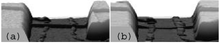
The MWNTs were synthesized by arc-discharge evaporation and carefully purified [16]. The MWNTs are sonicated in dichloroethane and dispersed onto an oxidized Si substrate. Atomic force microscopy is used to image, select and locate nanotubes that are then contacted with Cr/Au electrodes by electronic lithography. An example of a device is shown in Fig 1(a). Typical two-point resistances at low-bias vary in the range to k.
The electronic properties of different shells in a MWNT are probed using the electrical-breakdown method developed by Collins [14, 15]. The shells are selectively removed stepwise by injecting a large current in the MWNT. The bias voltage is increased until a sharp step in the current is detected that corresponds to the failure of one shell. Then, the bias voltage is quickly put down to 0 in ms. The removed shell has been shown to be the outermost one which is in direct contact with air and therefore most subject to a rapid oxidation initiated by the current [15]. We remove shells until no more current is detected. The final diameter has then decreased to typically nm as seen on the AFM picture in Fig. 1(b). The image shows that the peeling is uniform along the tube, except near the electrodes. Note that the failure is apparently different for the last shells since they are not evaporated. Failure may be local and situated at a small gap, too short to be observed with AFM.
We have designed an experiment where a series of electrodes is attached to a single long MWNT with various separations from to nm. Fig. 2(a-c) show the result of the electrical-breakdown method applied to the different sections of this MWNT. Let us first consider the current-voltage characteristics () of the pristine sample given by the upper curve. It appears that the high-bias current is significantly larger in the shortest section. This result can be enlightened by analyzing the current carried by the different shells of the MWNT that are obtained by comparing the successive s. Inspection of Fig. 2(a-c) shows that the current increase in the 200 nm section is the combined effect of more jumps and larger jumps.
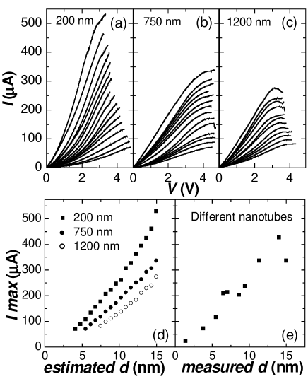
We discuss first the jump number. This 15 nm diameter MWNT is expected to consist of shells. The jump number is however smaller and dependent. It is reduced from 17 to 13 when passes from 200 to 1200 nm. A smaller number of jumps might be due to a smaller number of shells and to a thinner diameter. However, this is unlikely since AFM imaging indicates a uniform diameter over the entire length. This observation suggests rather that some shells do not participate to the current, especially in the longer sections. Such an interpretation is supported by the following observation in Fig. 2(d), where the maximum current of each is plotted as a function of the diameter . The diameter has not been measured by AFM at each step but estimated assuming that the diameter decreases each time by twice the interlayer distance Å. The extrapolated curves should pass by A at nm, the saturation of a SWNT. This is not the case. Rather, the extrapolations have negative current values at nm, which indicates that is overestimated and suggests that some shells do not participate to the current.
As mentioned before, the current jumps for the shortest length are larger in amplitude. The jump averages are 28.7, 19.1 and 17.4 A for respectively the 200, 750 and 1200 nm lengths. Remarkably, the curves in Fig. 2d deviate from a linear behavior. The deviation is best seen for the nm length. It shows that large-diameter shells contribute more to current. This finding has been observed in more than MWNTs. Other examples are shown in Fig. 3(a) and (b), where the current jump is plotted as a function of . Both curves show that is larger for larger . However, the slope is much weaker for the nm length and is hardly observed due the measurement noise.
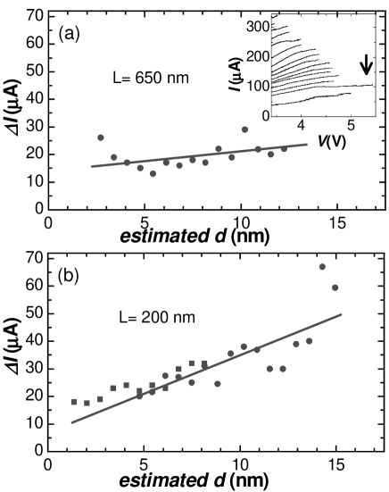
We note that an accurate determination of the current jump is difficult. Inset of Fig. 3(a) shows that the bias at which the shell fails increases irregularly and that the s are not smooth. We define the current-jump as the current difference at a bias given by the maximum voltage recorded for the two successive s. Another approach could have been to take the maximum of the difference or the difference of the maximums. However, the observation of a current increase with diameter is not altered by the choice of the estimation procedure. Importantly, the current jump estimation is precise enough to obtain close slopes of for different MWNTs with same length as seen in Fig. 3(b).
We now discuss the possible origins of these geometrical dependences in the shell current. We review first the electron-phonon scattering process that causes the current to saturate at A in metal SWNTs [12]. An electron that is accelarated by an electric field will gain energy until an optical phonon of energy is emitted ( 0.16eV). At this point, the coupling to the phonon is so strong that the electron is backscattered. Using a Landauer-type argument the current saturation is shown to be proportional to the phonon energy, A. The mean free path is equal to the distance an electron must travel to be accelerated to , [12]. The total transmission trough the whole tube is obtained by dividing by
| (1) |
where V is the voltage applied between the electrodes. Eq. (2) is valid for large .
At first sight, the current jump variations might be explained from the energy variation of phonons as a function of diameter. However, calculations have shown that optical phonon energy changes barely with tube diameter [17]. An alternative mechanism is thus needed to account for the current-jump variation.
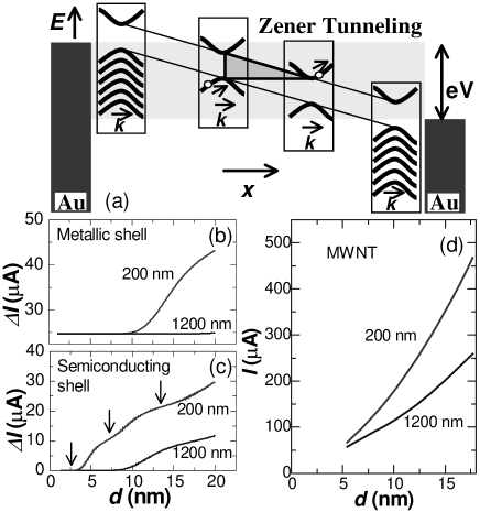
We propose that the current sensitivity to diameter results from the contribution of Zener tunneling [18]. Fig 4(a) shows a scheme that represents the potential variation in space of the band structure. The potential drop should be in principle determined by the self-consistent solution of the Poisson equation and the nonequilibrium electron density. We assume here that the voltage drop is linear, a good approximation when multiple electron-phonon scattering processes occur [19].
An electron that enters a non-crossing subband from the left electrode reaches at some point the top of the valence band and tunnels to the conduction band. The Zener-tunneling transmission [20] is given by
| (2) |
where we have assumed a linear voltage drop. is the effective mass and the gap that goes like .
Now, we compare the two transmissions as a function of diameter. The phonon transmission is independent on and at V. For a large semiconducting shell of nm diameter and nm, we obtain for tunneling between the upper valence band and the lower conduction band. The effective mass has been estimated using the thigh-binding model for a zig-zag tube. The comparison between and shows that the current is limited by phonons. Zener reflexion is here unimportant and no difference in current is expected between metal and semiconducting shells in agreement with experiment. The situation changes for small-diameter shells. For nm we estimate so that the current is now limited by Zener tunneling [21].
To put the above analyze on a more quantitative basis, we use the Landauer formula to estimate the high-bias current of a shell. Since the considered transmissions are weak, the total transmission of the subband is given by . is the energy separation between the valence band to the conduction band, where is counted from the neutrality point. Note that alternative processes such as tunneling from the valence band to the first conduction band changes barely the results presented below. The current is given by . The integral is calculated between and . The use of the Landauer formula in presence of inelastic scattering in the non-equilibrium regime is rather crude since it does not account for the exclusion principle. But it allows to give some physical insight. A model based on Boltzmann equation as in [12] that incorporates Zener tunneling is probably needed for more accuracy.
Fig 4(b) and (c) show the calculated current as a function of diameter of metal and semiconducting shells. The current increases with diameter and decreases with length, in agreement with experiment. Indeed, larger diameters decrease the subband gap and enable better Zener transmission. Similarly, the tunneling transmission becomes weaker for longer nanotubes as the Zener barrier length increases.
Fig. 4(d) shows the calculated current as a function of the diameter of MWNTs. We assume that MWNTs consist of shells that carry current in parallel. The current through the MWNT is the sum of the current of a series of shells with diameter ranging from nm to . For each shell an average is taken on the current of a semiconducting and a metal shell with the statistical weights . The resemblance to the experiment is remarkable. parameter has been used[22].
Here, we discuss the number of subbands within a shell that carry significantly current. The calculated curve in Fig. 4c has 3 plateaus indicated by arrows. They correspond to situations where 0, 1 and respectively 2 subbands carry current. These subbands are close to the neutrality point and the Zener barrier is negligible compared to phonon scattering, . The other subbands that have no contribution to the current correspond to deeper valence bands with large . Zener reflection has thus a dramatic role in the high bias transport in MWNTs. About subbands in a nm shell are counted for V and have to be taken into account for the current estimation, but very few contribute effectively.
Fig. 4(c) shows the current of semiconducting shells as a function of diameter. It appears that thin diameter shells do not carry current. This happens when . Moreover, the diameter at which semiconducting shells start to conduct becomes larger for longer tubes. This may explain the discussed experimental observation that the number of jumps is reduced for longer section. Such an interpretation is further supported as follows. Inset of Fig. 3(a) shows that the indicated by an arrow fails at a bias larger than the others. Such s have been observed several times but mostly for the last . At the failure the current is typically A and corresponds to several shells. We propose that the outermost shell is semiconducting in this situation and do not carry current. The current has to pass through inner shells that are protected from oxygen and that can sustain higher voltages. At the failure, the breakdown is mostly so violent that all the shells fail together.
We finish with a discussion on the performances of large-diameter MWNTs as interconnects. We have shown that the number of current-carrying subbands within a shell depends weakly on the diameter and the length and stays typically close to one. Thus, the current saturation of MWNTs is expected to vary roughly linearly with the shell number and thus the diameter. This is observed in Fig. 2(e), where the maximum current as a function of diameter is plotted for 10 samples. The functional form is not quadratic as it would be expected for a plain wire. This makes current-carrying capacities of MWNTs less efficient as interconnects when they become larger. However, the current carrying capacity of large MWNTs still surpasses Cu wires ( A/cm2). For example, the current of a nm diameter MWNT is estimated to be times larger.
The authors wish to thank N. Regnault, P. Morfin and C. Delalande. The research has been supported by the CNRS, DGA, ACN programs, Paris and Paris .
∗ corresponding author: bachtold@lpmc.ens.fr
REFERENCES
- [1] M. S. Fuhrer , Science 288, 494 (2000).
- [2] Z. Yao, H. W. C. Postma, L. Balents, and C. Dekker, Nature 402, 273 (1999).
- [3] S. J. Tans, A. R. M. Verschueren, C. Dekker, Nature 393, 49 (1998).
- [4] R. Martel , Appl. Phys. Lett. 73, 2447 (1998).
- [5] A. Bachtold, P. Hadley, T. Nakanishi, C. Dekker, Science 294, 1317 (2001).
- [6] V. Derycke, R. Martel, J. Appenzeller, P. Avouris, Nano. Lett. 1, 453 (2001).
- [7] X. Liu , Appl. Phys. Lett. 79, 3329 (2001).
- [8] P.L. McEuen, M.S. Fuhrer, H. Park, IEEE Trans. on Nanotech. 1, 78 (2002).
- [9] B.Q. Wei, R. Vajtai, P.M. Ajayan, Appl. Phys. Lett. 79, 1172 (2001).
- [10] F. Kreupl , Microelectron. Eng. 64, 399 (2002)
- [11] J. Li , Appl. Phys. Lett. 82, 2491 (2003).
- [12] Z. Yao, C.L. Kane, C. Dekker, Phys. Rev. Lett. 84, 2941 (2000).
- [13] This is in contrast to low-bias and low-temperature measurements. A. Bachtold , Nature 397, 673 (1999).
- [14] P. G. Collins, M. S. Arnold, Ph. Avouris, Science 292, 706 (2001).
- [15] P. G. Collins , Phys. Rev. Lett. 86, 3128 (2001).
- [16] J.M. Bonard, , Adv. Mater. 9, 827 (1997).
- [17] O. Dubay, G. Kresse, Phys. Rev. B 67, 035401 (2003).
- [18] M.P. Anantram, Phys. Rev. B 62, R4837 (2000).
- [19] The voltage drops are neglected at the nanotube-electrode interface. Indeed large contact resistances are observed to have no influence on the current saturation.
- [20] S.M. Sze, in , (Wiley Interscience, 1981).
- [21] For nm, meV and kg. For nm, meV and kg.
- [22] The calculations show that the current does not really saturate for short tubes such as nm long in contrast to the longer ones. The calculations reproduce well the s shown in Fig. 1(a-c).