[
Gate-Induced Mott Transition
Abstract
For a strongly correlated material, VO2, near a critical
on-site Coulomb energy =1, the abrupt Mott metal-insulator
transition (MIT) rather than the continuous Hubbard MIT is
observed by inducing internal optical phonon-coupled holes (hole
inducing of 0.018) into conduction band, with a gate field of
fabricated transistors. Observed gate effects, change of the MIT
drain-source voltage caused by a gate field, are the effect of
measurement due to inhomogeneity of channel material and is an
average over the measurement region of the true gate effect based
on the large conductivity (or effective mass) near the MIT
predicted by the Brinkman-Rice picture. A discontinuous gate
effect such as digital is observed, which is a characteristic of
the transistor and a possible condition of a very high-speed
switching transistor.
PACS numbers: 71.27. +a, 71.30.+h
] In a strongly correlated system, a metal-insulator transition (MIT) near a critical on-site Coulomb energy, =1, has long been controversial in terms of whether the transition is Mott’s abrupt (or first-order) MIT or Hubbard’s continuous (or second-order) MIT . This is because it is unclear whether experimental observations of the abrupt MIT (Mott transition) follow Mott’s prediction, although a first-order MIT with temperature was observed by McWhan . Rather than the abrupt MIT, Boriskov and Kumai measured the nonconduction-conduction transition (NCT) with an electric field for VO2 and an organic material, respectively. Oka found the NCT with an electric field could be described in terms of a universal Landau-Zener quantum tunnelling through a theoretical consideration based on the Hubbard model. Newn regarded the NCT in a Mott-Hubbard insulator as the Hubbard MIT for a transistor based on the NCT. However, the Mott MIT, which differs from the NCT, has not been observed for a very low doping of charges (hole content of 0.018 for VO2), as predicted by Mott . The very low doping is a decisive key determining an order (first or second) of two kinds of the MIT.
An abrupt MIT breaks down an energy gap between sub-bands in a main band. The energy gap is formed by a strong correlated on-site Coulomb energy. The abrupt MIT in a strongly correlated metal with an electronic structure of one electron per atom was theoretically demonstrated by Brinkman and Rice; this is called the Brinkman-Rice (BR) picture . The abrupt MIT with band filling was also developed through extension of the BR picture by Kim . The extended BR picture was based on a fractional charge justified by means of measurement in an inhomogeneous metallic system .
In this letter, we observe the abrupt MIT (or Mott transition), inducing internal optical phonon-coupled hole charges (hole content of 0.018) into conduction band with a gate field of a fabricated field-effect transistor. This reveals a difference between the abrupt MIT and the continuous MIT. Note that artificial hole doping of 0.018 is not possible other than the method applying the gate field.
In the extended BR picture , the effective mass, , of a carrier is given by
| (1) |
where is the bare electron mass, is , is the strength of Coulomb energy between carriers when =1, and 0 is band filling. When , Eq. (1) is well fitted in a real metallic system and the effect of measurement (or average) for an inhomogeneous system . An electric conductivity, .
The material at =1 in Eq. (1) can be assumed as a paramagnetic insulator (or Mott insulator). The metal at a critical value (=) of just below =1 shows the best metallic characteristics . The MIT from a metal at both and =1 (1) to the insulator at both =1 and =1 (=1) is abrupt (or a jump); this is an idea for observing the Mott transition near =1. Holes corresponding to the difference (critical hole content, ) between and =1 are induced into a conduction band having electrons by a gate electric field; this is regarded as the decrease of the Coulomb energy . Then, the energy gap breaks down and the metallic system becomes inhomogeneous because of the induced holes . The number of the induced holes can be regarded as , predicted by Mott from 0.25 . Here, is the Bohr radius and corresponds to about 0.018 of the number of carriers in the half-filled band, when one electron in the cell volume, 59.2210-24 cm3, of VO2 is assumed; =0.018. Further, a gate electric field of a transistor induces holes in optical phonon-coupled-hole levels in a Mott insulator, a channel material, into conduction band . The process in which optical phonon-coupled holes change to carriers has been revealed . The hole levels are attributed to impurities such as oxygen deficiency, which indicates that VO2 is inhomogeneous, as proved experimentally by Kumai .
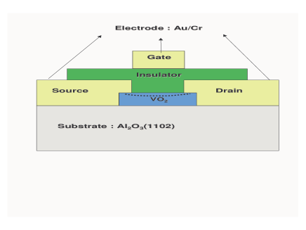
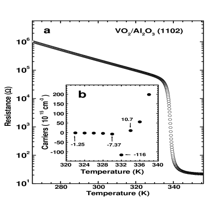
We fabricate transistors to observe the Mott transition on the basis of the above theory. The schematic diagram of the transistor is shown in Fig. 1. Thin films of the Mott insulator, VO2, with a sub-energy gap of about 1 in the -main band have been deposited on Al2O3 substrates by laser ablation. The thickness of the VO2 film is about 900. The resistance of the film decreases with increasing temperature and shows an abrupt MIT at a transition temperature, =340 K (68∘C) (Fig. 2a). This is the same as that measured by Borek . The decrease of the resistance up to 340 K indicates an increase of hole carriers, and two kinds of electron and hole carriers coexist near =340 K (Fig. 2b). From 332 to 340 K, the number of carriers is not clear because of mixing of electrons and holes. We speculate that the number of hole carriers can be at =340 K on the general basis that an exponential decrease of the resistance with temperature in semiconductor physics indicates an exponential increase of carriers. In the metal regime above 340 K, carriers are electrons (Fig. 2).
Gate insulators, amorphous Ba0.5Sr0.5TiO3 (BSTO), Si3N4 and SiO2 were used. BSTO and Si3N4 were deposited on the VO2 film at a VO2 surface temperature, 400∘C and 150∘C, respectively. The thickness and the dielectric constant of the BSTO and Si3N4 films were about 1200, 43 and 2000, 7, respectively. Transistors of channel length, = 3, and gate width, , were fabricated by lithography processes. The gate width of a transistor based on Si substrate is . Au/Cr electrodes were prepared for Ohmic contact. Characteristics of the transistors were measured by a precision semiconductor parameter analyzer (HP4156B). To protect transistors from excess current, the maximum current was limited.
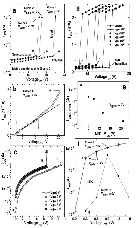
Figure 3a shows the drain-source current, , vs the drain-source voltage, , characteristics of transistor 1 with a gate insulator of BSTO. The measured gate current, , between the gate and the source is an order of 10 at gate voltages of =0, -2 and -10V, which indicates that there is sufficient insulation between the gate and the source. Fig. 3b shows a NCT below the MIT- of point A of curve 1 measured by an applied electric field between the source and the drain at VG=0V. This was observed by using a two-terminal structure by Boriscov and Kumai who used an organic Mott-insulator. The two groups suggested that the NCT occurs due to an applied field and an induced current , not an increase of sample temperature due to leakage current. The abrupt MIT of curve 1 has been measured more than 1,500 times without breakdown. follows the Ohmic behavior up to 12V, but shows nonlinear electric conduction in the total regime below the MIT- of point A (Fig. 3b). The nonlinear conduction behavior is regarded as semiconducting behavior due to the increase of hole carriers by Zener’s impact ionization, as observed by the Hall effect (Fig. 2b). It was revealed through a theoretical consideration that the Ohmic behavior is described in terms of a universal Landau-Zener quantum tunnelling [8]. The NCT is an insulator-semiconductor transition. We suggest that the abrupt MIT at point A occurs when the number of hole carriers produced by impact ionization becomes the number of predicted by Mott. The semiconduction in Fig. 3a is regarded as the doping process in which (or ) of holes are induced by electric field. Moreover, at the jumped point in curve 1, the current density is about =3105 A/cm2, which is current collective motion observed in metal.
Curves 2 and 3 are vs characteristics measured at gate voltages, VG= -2 and -10, respectively. The abrupt MITs also occur at transition points B and C. The sharp transitions indicate that transistor 1 was well fabricated. The abrupt MIT at point B, which is caused by the induced charges of , occurs suddenly at =-2V, such as digital, as indicated in Eq. (1). This is the most unique characteristic of this transistor. The gate effect, a change of the MIT- caused by a gate field, is small, which is that the channel material in the measurement region is inhomogeneous (see, ). When only homogeneous region is measured, the true gate effect becomes maximum due to the maximum conductivity (or the maximum effective mass) near the MIT as indicated in the BR picture; MIT- 0. The gate effect increases as homogeneity of the VO2 film increases. Thus, the observed gate effect is an average of the true gate effect over the measurement region. (or ) may be attained by the gate effect and the impact ionization on the ground of the large transition .
Figure 3c shows current-voltage characteristics of transistor 2 with a gate insulator of an amorphous Si3N4. The gate-source current is 3.610-12A through the Si3N4 at =-2V and =0.1V. An off-current is 1.310-7A at point D. The abrupt MITs occur at point F of =13V (or =4.3MV/m) at =0V and point G of =9V (or =3MV/m) at =-2V. The gate effect at point G at =-2V is similar to that of transistor 1; there is no gate effect at -2V0. The discontinuous gate effect is a possible condition of a very high-speed transistor. Namely, transconductance related to a switching speed can be regarded as maximum.
Figure 3d shows vs near the abrupt MIT of transistor 3 with a gate insulator of SiO2. Its structure is a VO2/SiO2/WSi/Si substrate. Its characteristics are given as follows. First, the gate effect at =14V and =-10V, is due to hole inducing of ; this is the abrupt MIT with band filling near =1 in Eq. (1) and due to the jump of the gate voltage. Second, the MIT- increases with an increasing negative gate voltage (or field), which is the decrease of the conductivity (or the effective mass in Eq. (1)); this is due to the continuous change of the gate voltage. Moreover, the increase of the inducing hole content greater than the critical content, , decreases and the electrical conductivity, , because of ; is maximum at . From current density of =, an electric field, , increases with a decreasing to constant ), as shown at transition points in Figs. 3a, 3c and 3d, ; . We also observed that the MIT- decreases with an increasing positive gate voltage. Third, in the metal regime over =2mA shows Ohmic’s law which differs from the behavior in Fig. 3b. At the jumped point, current density is =0.9105 A/cm2, which is current collective motion measured in metal. Thus, Fig. 3d follows the behavior of Eq. (1) when =1.
We suggest conditions of a good transistor fabrication by comparing transistors 1 and 2. The off-current ( at a very low and =0V) and the MIT-VDS values of transistor 1 are lower and higher, respectively, than those of transistor 2; =20.8V (or =7MV/m) of point A and =13V (or =4.3 MV/m) of point F. The smaller VDS results from the higher off-current arising from an oxygen deficiency of VO2 when the gate insulator is deposited. The off-current is caused by the excitation of the optical phonon-coupled holes. When the number of total holes in the hole levels is given by , where is the number of optical phonon-coupled holes and is the number of holes freed from the levels, decreases with increased , because is constant. In oxide materials, is about 5.510 which corresponds to 0.034 to -band charges . The larger off-current is attributed to the increase of . For the abrupt MIT, =0 should be satisfied, where , as predicted by Mott. Hence, the decrease of contributes to the reduction of the MIT- (Fig. 3e). In Fig. 3c, the smaller MIT- of transistor 2 is due to the smaller = induced by the gate electric voltage (field) than that of transistor 1. For a good transistor, off-current can be decreased when the deposition temperature or oxygen content of VO2 film is slightly increased. In addition, when gate length is less than 100nm, is much less than 1V.
Figure 3f shows the magnified part below =1.5V of the curves in Fig. 3a. A current signal such as noise in curve 1 without is measured when the resistance of the VO2 film between the source and the drain is large. When are applied, curves 2 and 3 show a high gain current of about 250 times at =0.3V, which is the gate effect observed in a semiconductor transistor. The high gain represents a significant difference between this transistor with the abrupt MIT and the Mott transistor developed with a Mott-Hubbard insulator, Y1-xPrxBa2Cu3O7-δ, by Newn’s Although they regard a transition for the Mott transistor as the Hubbard MIT, the transition is the NCT. Their transistor is not the Mott transistor.
In conclusion, the abrupt Mott MIT near =1 is first observed by inducing of internal holes of 0.018 with gate fields, while the continuous Hubbard MIT does not exist in Mott and Mott-Hubbard insulators. Generally, the reason that the continuous MIT is observed in strongly correlated systems including high- superconductors is because the continuous behavior in both Eq. (1) and Fig. 3d is observed when a doped content, . The measured gate effects predicted by Eq. (1) due to inhomogeneity of channel material is an average of the true gate effect. Furthermore, the transistor developed here is a true Mott transistor without short channel effects proposed in metal-oxide-semiconductor field-effect transistors and will be very useful for nano-devices.
We thank Dr. Soo-Hyeon Park at KBSI for Hall-effect measurement, Dr. Gyungock Kim for valuable discussions on the Zener transition, and Dr. J. H. Park for fabrication of Si3N4 films by using CVD. HT Kim, the leader of this project, developed the concept, and wrote the paper. BG Chae and DH Youn deposited VO2 and BSTO films, performed the transistor fabrication process, and measured characteristics. KY Kang prepared the laser-ablation and lithography equipment and generated this project with HT Kim. SL Maeng evaluated transistor characteristics, the shielding measurement system, and Si3N4 film fabrication.
REFERENCES
- [1] htkim@etri.re.kr, kimht45@hotmail.com
- [2] N. F. Mott (Taylor and Frances Press, 1990).
- [3] X. Y. Zhang, M. J. Rozenberg, and G. Kotliar, Phys. Rev. Lett. 70, 1666 (1993).
- [4] M. Imada, A. Fujimori, and Y. Tokura, Rev. Mod. Phys. 70, 1039 (1998).
- [5] F. Fazekas (World Scientific Press, 1999).
- [6] D. B. McWhan, T. M. Rice, and J. P. Remeika, Phys. Rev. Lett. 23, 1384 (1969).
- [7] P. P. Boriscov, A. A. Velichko, A. L. Pergament, G. B. Stefanovich, and D. G. Stefanovich, Techni. Phys. Lett. 28, 406 (2002).
- [8] R. Kumai, Y. Okimoto, and Y. Tokura, Science 284, 1645 (1999).
- [9] T. Oka, R. Arita, and H. Aoki, cond-mat/0304036.
- [10] D. M. Newns, J. A. Misewich, C. C. Tsuei, A. Gupta, B. A. Scott, A. Schrott, Appl. Phys. Lett. 73, 780 (1998).
- [11] W. F. Brinkman, T. M. Rice, Phys. Rev. B2, 4302 (1970).
- [12] H. T. Kim, Physica C 341-348, 259 (2000).
- [13] H. T. Kim, (Kluwer Press, 2002), NATO Science Series Vol. II/67, p. 137; cond-mat/0110112.
- [14] Y. Tokura , Phys. Rev. Lett. 70, 2126 (1993).
- [15] I. L. Botto, M. B. Vassallo, E. J. Baran, and G. Minelli, Mater. Chem. Phys. 50, 267 (1997).
- [16] H. T. Kim, H. Minami, and H. Uwe, (Springer-Verlag Press, 1995) p. 169; cond-mat/0303442.
- [17] S. M. Sze, Chapter 7, (John Wiley and Sons, 1981).
- [18] R. Zimmermann, R. Claessen, F. Reinert, P. Steiner, and S. Hfner, J. Phys.: Condens. Matter 10, 5697 (1998).
- [19] M. Borek, F. Qian, V. Nagabushnam, and R. K. Singh, Appl. Phys. Lett. 63, 3288 (1993).
-
[20]
K. Sega, H. Kasai, and H. Sakata, Mater. Chem. Phys. 53, 28
(1998).