Drain Voltage Scaling in Carbon Nanotube Transistors
Abstract
While decreasing the oxide thickness in carbon nanotube field-effect transistors (CNFETs) improves the turn-on behavior, we demonstrate that this also requires scaling the range of the drain voltage. This scaling is needed to avoid an exponential increase in Off-current with drain voltage, due to modulation of the Schottky barriers at both the source and drain contact. We illustrate this with results for bottom-gated ambipolar CNFETs with oxides of 2 and nm, and give an explicit scaling rule for the drain voltage. Above the drain voltage limit, the Off-current becomes large and has equal electron and hole contributions. This allows the recently reported light emission from appropriately biased CNFETs.
Recently, it has been shown experimentally [5, 6] as well as theoretically [7, 8] that typical carbon nanotube field-effect transistors (CNFETs) [9] operate by changing the transmissivity of the Schottky barrier (SB) at the contact between the metal electrode and the nanotube (NT). Due to the sharp edge at the metal-NT contact and the quasi 1D-channel of the NT, this barrier can be thinned sufficiently with gate voltage to allow thermally-assisted tunneling of electrons or holes. This working principle has important implications for device performance, e.g. it leads to a different scaling of the turn-on gate voltage with oxide thickness than for conventional transistors.[6, 10]
Typically, CNFETs have had thick gate oxides, requiring large gate voltage for turn-on, and could be operated at drain voltages of V or more. The performance of CNFETs can be systematically improved by reducing the thickness of the gate oxide.[6, 10, 11, 12] However, we find that this places new constraints on the drain voltage. If the drain voltage is not scaled appropriately, reducing the oxide thickness can lead to minority-carrier injection at the drain, giving unacceptable Off-currents. The simultaneous electron and hole currents in this regime are of great interest for light-emission devices,[13] which have requirements opposite to SB-CNFETs. We derive explicit requirements for drain voltage scaling to obtain optimal device performance.
Our back-gated CNFET devices are produced using a two-step oxidation process which allows the formation of small ultra-thin oxide areas on which NTs are contacted, while keeping most of the substrate covered with thicker field oxide. The fabrication begins with nm thick silicon nitride on top of a degenerately doped silicon wafer which serves as the backgate. Electron beam lithography (EBL) and reactive ion etching are used to pattern and remove the nitride except in micrometer-sized areas. The exposed silicon is covered by nm thick, thermally grown field oxide. Silicon nitride is dissolved in phosphoric acid, and precisely controlled dry oxidation is used to deposit another nm or nm of silicon dioxide. Carbon nanotubes[14] are dispersed on these substrates, and source and drain connections to NTs located in areas of thin oxide are patterned using standard EBL and lift-off.
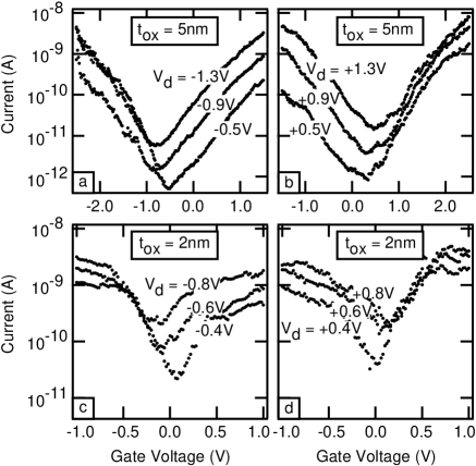
We focus on ambipolar devices, in particular those where the Fermi level at the metal-NT contact falls in the middle of the bandgap. Figure 1 shows typical transfer characteristics of current () vs. applied gate voltage () for different drain voltages () and oxide thicknesses (). All curves show the typical ambipolar characteristics, with hole current to the left of the minimum and electron current to the right. The gate voltage for minimum current shifts noticeably with drain voltage. Furthermore, we observe that at positive the curves almost overlap for the electron current while they split for the hole current, and vice versa for negative .
The minimum current as a function of , i.e. the Off-current (), rises steeply with increased absolute value of . While the Off-current increase is clear in CNFETs with nm, it is particularly worrisome for devices with nm where performance deteriorates already at V. (We note for comparison that the concurrently measured current leakage between the gate and source/drain electrodes are below fA and pA for CNFETs with nm and nm, respectively.)
In order to understand these observations we use a semiclassical approach to calculate the total current through the device. For ballistic transport in the NT,[15] we can calculate the current with the Landauer-Büttiker formula:
| (1) |
where is the Fermi function. The energy-dependent transmission through the device is controlled by the SBs at the source and drain contact. The transmission through the SBs are evaluated within the WKB approximation, using the idealized band structure [16] for a NT with EeV and diameter of nm.
The shape of the SBs at the source and drain contact depend on the electrostatic potential along the NT. We calculate the potential by solving the Laplace equation for a device geometry with a bottom gate at from the NT and a grounded top electrode which is far from the NT. Neglecting charge on the NT is a good approximation for the Off-state and the turn-on regime.[7, 10]
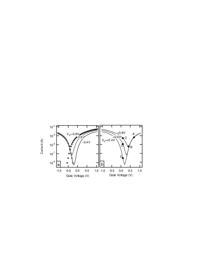
Figure 2 shows the calculated transfer characteristics at various drain voltages, for a device geometry as in the experiment. The effect of drain voltage on the current characteristics for ideally ambipolar devices is clearly captured by the model. We see the splitting of the curves for the electron branch at negative and for the hole branch at positive as in the experiment. Moreover, in the model, the gate voltage giving minimum current is exactly half the applied drain voltage, and the current is symmetric about this gate voltage . The shift of the current minimum in the experiment, Fig. 1, is in approximate agreement with this prediction. (The quantitative current is sensitive to details of the contact geometry, and the sharper turn-on in the theory may result from an assumed geometry more favorable than the actual one.[10])
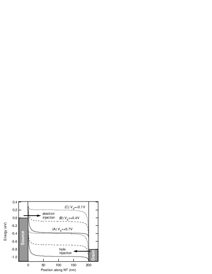
Calculated band diagrams for different voltage regimes are displayed in Fig. 3. In the long channel limit () the electric field, as well as the transmissivity of the source and drain contacts, should only depend on the two potential differences and . In a sense, the device acts as two SBs connected by a field-free region in the bulk of the nanotube. At large positive , labeled by point A in Fig. 2(b) and the solid line in Fig. 3, the CNFET is in the On-state. Because at point A, the band bending at the drain is insignificant, and the current is controlled by the source barrier.[7, 8] As the gate voltage is decreased, the SB at the source becomes wider and thus the electron tunneling current is lowered. However, the potential drop at the drain electrode, , increases. At (B) both SBs have the same shape and there is an equal contribution of electron and hole injection. If is close to or above the turn-on voltage, these currents can be significant and the device cannot be turned off. (In this regime, electron-hole recombination can lead to polarized light emission from an individual semiconducting nanotube.[13])
For symmetric source and drain contacts, as in the calculation, the electron current rises monotonically with exactly as the hole current increases monotonically with , Fig. 2(a). Therefore, the total current becomes minimal at . As the gate voltage is further decreased (C) the hole current at the drain dominates the current through the device. This drain field induced current results in a severely deteriorated Off-current. We calculate that for V, the On/Off ratio () decreases from about at nm to less than at nm.
However, for operation of the devices as transistors an On/Off ratio of about is desirable. Using an analytic model for the scaling of the current with [10], we obtain an explicit rule for to meet this criterion. The upper limit is given by V for the simulated bottom-gate devices. The scaling as is a consequence of the same scaling for the turn-on voltage.[10] (For experimental CNFETs the allowed may be a little larger due to a less favorable contact geometry, but the same scaling rule will still hold.) For nm, we find that to have an On/Off ratio of at least requires V.
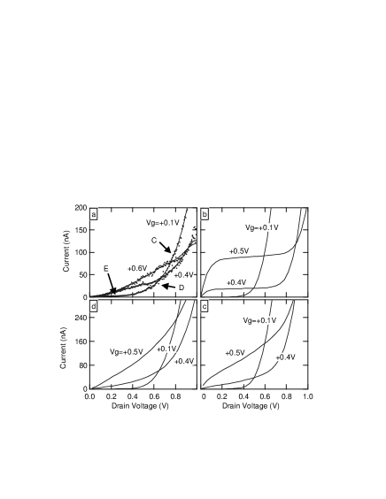
The drain voltage induced minority carrier current also affects the device output characteristics ( vs. ) as shown in Fig. 4(a). Instead of being Off near zero gate voltage [regimes D and E in Figs. 2 and 4(a)], a large potential difference at the drain induces an exponential increase of the current (regime C) in the device. This can result in crossing of vs. at different values of , a behavior not observed in conventional transistors. The corresponding increase in Off-current puts an upper bound on the useable range of at about V, in agreement with our estimate for the feasible On/Off ratio.
Figure 4(b) shows that the general crossover trend of vs. curves at different is captured by the simulations of a long channel device which mirrors the geometry of the measured CNFET. However, the experimental data more closely resembles the short-channel device obtained when the NT length is decreased (from nm) to nm [Fig. 4(c)]. Apparent short-channel effects in our devices occur at larger ratios than in the simulations, perhaps due to differences in geometry, or to other unrecognized effects. The closest agreement [Fig. 4(d)] can be obtained by assuming that the impact of the gate is slightly better at the source than the drain, due to e.g. slight variations in oxide thickness or contact geometry. It is important to note that while these details of the geometry affect the output characteristics, they do not change our conclusions on the exponential increase in Off-current or the splitting of the vs. curves with .
Our discussion has been limited to a midgap line-up of the metal Fermi energy with the NT bands, and a bandgap of eV. However, we confirmed that the drain voltage induced current is a significant issue for ultra-thin oxide CNFETs even for asymmetric line-ups or different band gaps. Thus the limit in drain voltage will scale quite generally as the turn-on gate voltage, which gives a square-root scaling for the device geometries we have studied. [10] Above the drain voltage limit, the device can be used as a light source [13] by operating it at the Off-voltage () where the current consists of equal electron and hole contributions.
We thank Jörg Appenzeller for valuable discussions, Shalom Wind for experimental advice, Jim Bucchignano for e-beam lithography and Bruce Ek for expert technical assistance. The devices were prepared with help of ASTL and CSS facilities at T. J. Watson Research Center. S. H. thanks the Deutsche Forschungsgemeinschaft for financial support under Grant number HE3292/2-1.
REFERENCES
- [1]
- [2] These authors contributed equally to this work.
- [3] Electronic address: tersoff@us.ibm.com
- [4] Electronic address: avouris@us.ibm.com
- [5] R. Martel, V. Derycke, C. Lavoie, J. Appenzeller, K. K. Chan, J. Tersoff, and Ph. Avouris, Phys. Rev. Lett. 87, 256805 (2001).
- [6] J. Appenzeller, J. Knoch, V. Derycke, R. Martel, S. J. Wind, and Ph. Avouris, Phys. Rev. Lett. 89, 126801 (2002).
- [7] S. Heinze, J. Tersoff, R. Martel, V. Derycke, J. Appenzeller, and Ph. Avouris, Phys. Rev. Lett. 89, 106801 (2002).
- [8] T. Nakanishi, A. Bachtold, and C. Dekker, Phys. Rev. B 66, 073307 (2002).
- [9] S. J. Tans, A. Verschueren, and C. Dekker, Nature (London) 393, 49 (1998); R. Martel, T. Schmidt, H. R. Shea, T. Hertel, and Ph. Avouris, Appl. Phys. Lett. 73, 2447 (1998).
- [10] S. Heinze, M. Radosavljević, J. Tersoff, and Ph. Avouris, cond-mat/0302175.
- [11] A. Bachtold, P. Hadley, T. Nakanishi, and C. Dekker, Science 294, 1317 (2001).
- [12] A. Javey, H. Kim, M. Brink, Q. Wang, A. Ural, J. Guo, P. McIntyre, P. McEuen, M. Lundstrom, and H. J. Dai, Nature Mat. 1, 241 (2002).
- [13] J. A. Misewich, R. Martel, Ph. Avouris, J. C. Tsang, S. Heinze, and J. Tersoff, Science 300, 783 (2003).
- [14] The nanotubes with mean diameter of nm were grown by laser ablation as described in A. Thess et al., Science 273, 483 (1996). They were used without further processing and dispersed in dichloroethane by a brief exposure to ultrasound.
- [15] M. Fuhrer, H. Park, and P. L. McEuen, IEEE Trans. Nanotech. 1, 78 (2002).
- [16] J. W. Mintmire, and C. T. White, Phys. Rev. Lett. 81, 2506 (1998).