Surface Junction in Bi2Sr2CaCu2O8+d Single Crystals
Abstract
As nature junction geometry of the -wave cuprate superconductor/insulator/the mixture of -wave and -wave cuprate superconductor, the upmost surface junction of intrinsic Josephson junction stack fabricated on Bi2Sr2CaCu2O8+d single crystals was measured and discussed. We successfully observed half-integral microwave induced steps as well as integral steps with resistively shunting technology, which shows the evidence of second order supercurrent, consistent with Tanaka’s theory.
pacs:
74.50.+r, 74.72.Hs, 74.80.DmPairing symmetry in the cuprate superconductor is an important and controversial topic. The recent development of phase-sensitive test, combined with the refinement of several other symmetry-sensitive techniques, has for the most part settled this controversy in favor of predominantly -wave symmetry for a number of optimally hole- and electron-doped cuprates Tsuei00 . Especially for Bi2Sr2CaCu2O8+d (BSCCO), the phase-sensitive test results suggest that the -wave component of the order parameter should be vanishingly small Kirtley96 . Considering the crystal structure of BSCCO, -wave and -wave pair states correspond to two distinct irreducible representations and therefore are not allowed to mix Klemm98 . As a result, BSCCO should be pure -wave pairing symmetry. However, a few -axis tunneling experiments between BSCCO and -wave superconductor Pb (BSCCO/Pb junction) consistently unveiled the finite supercurrent of first order. The results show -wave component in BSCCO should be small but nonzero Kleiner97 ; Mossle99 . However, the evidence of -wave is proven only in the upmost cuprate layer which couples to Pb. The question raised from the contradiction is: Is the -wave component intrinsic or induced from -wave state under some specific condition? Theoretical studies suggest that -wave paring symmetry may be induced in a d-wave superconductor, under certain conditions, by spatial inhomogeneities such as surfaces, interfaces, or defects Alvarez96 ; Zapotocky97 ; Martin98 ; Zhu98 . Reasonable explanation is that the -wave component of pairing state exists only in the surface cuprate layer of BSCCO, which is induced from -wave state by the surface effects.
According to a theory by Tanaka, second order -axis pair tunneling is possible for a junction between -axis -wave and pure -wave superconductors Tanaka94 . In other words, half-integer Shapiro steps should be observable in such a junction under microwave irradiation. In the results of -axis BSCCO/Pb junctions so far reported, the observed supercurrent is dominantly of first order, and microwave induced Shapiro steps only occur at voltages . Same results have also been observed in other junctions of similar type Sun94 ; Kleiner96 ; Lesueur97 ; Woods99 . In essence, all the junctions mentioned above are coupled by the -axis pairing tunneling between -wave conventional superconductor and the cuprate superconductor with the mixture of -wave and -wave pairing symmetry (s/I/s+d), which was discussed theoretically in detail Tanaka97 . Nevertheless, the -axis pairing tunneling between the -wave cuprate superconductor and the cuprate superconductor with the mixture of -wave and -wave pairing symmetry (d/I/s+d) has not been discussed yet both in theory and experiment. Natural geometry of d/I/s+d junction, noteworthy but neglected, is the upmost surface junction of intrinsic Josephson junction (IJJ) stack fabricated on BSCCO single crystals, which was discussed in a few papers without consideration of the mixture of -wave states and -wave states Kim99 ; Doh00a ; Doh00b . In this letter, we report and discuss the measurements of the surface junction and the observation of microwave induced steps with resistively shunting method.
BSCCO single crystals were grown using floating zone technique in a four lamp arc-imaging furnace. After cleaving from a bulk crystal, the fresh surface was deposited with a 70 nm layer of gold to obtain a clean surface between single crystal and normal electrode as well as to protect the surface from any contamination during further process of fabrication and measurements. To make the contact resistance ohmic, the cleaved flake was annealed in fresh O2 flow for 10 minutes at 6000C, then it was fixed on Si substrate by Polyimide. With conventional photolithography and Ar ion etching, one mesa with - plane sizes of covered with gold and photoresist was formed. The junction number in the stack is controlled by the etching time and rate. Finally a layer of SiO was deposited as insulator to protect and separate the mesa. After lift-off, one electrode was connected to the top gold of the mesa, while two other electrodes were connected to the ground plane of the mesa. All the transport measurements described below were carried out with three-probe configuration.
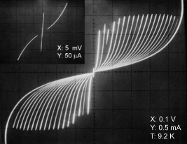
In our experiments, the samples were measured in a liquid helium Dewar flask. Shown in Fig. 1 is the typical curve of the samples. The multiple quasi-particle branches were developed with the increase of bias current. The junction number is counted as 20 corresponding to the number of the branches. The critical current Ic of most junctions is nearly 1.5 mA at 9.2 K except one, the critical current I of which is only 0.11 mA, one magnitude order smaller than the majority. The curve of this novel junction is magnified and shown as the inset of main figure. Its supercurrent is a little slantwise due to the linear contact resistance. This junction disappeared when the temperature rose to T=30K (35%Tc, Tc is the critical temperature of the bulk crystal.) Doh etc. proved by progressively ion-beam etching experiment that the novel junction is the upmost surface junction which forms by the upmost two cuprate layers Doh00a . The d-wave states in cuprate superconductor may induce to -wave states by spatial inhomogeneities such as surfaces, interfaces, or defects. As a result, the pairing symmetry of the upmost cuprate layer changes from -wave states to s+d mixed states with broken time-reversal symmetry due to the effect of surface. Moreover, the superconductivity of the upmost cuprate layer is also suppressed. Consequently, the critical temperature and critical current of the surface junction with the structure of d/I/s+d are greatly suppressed in comparison with the conventional d/I/d IJJ.
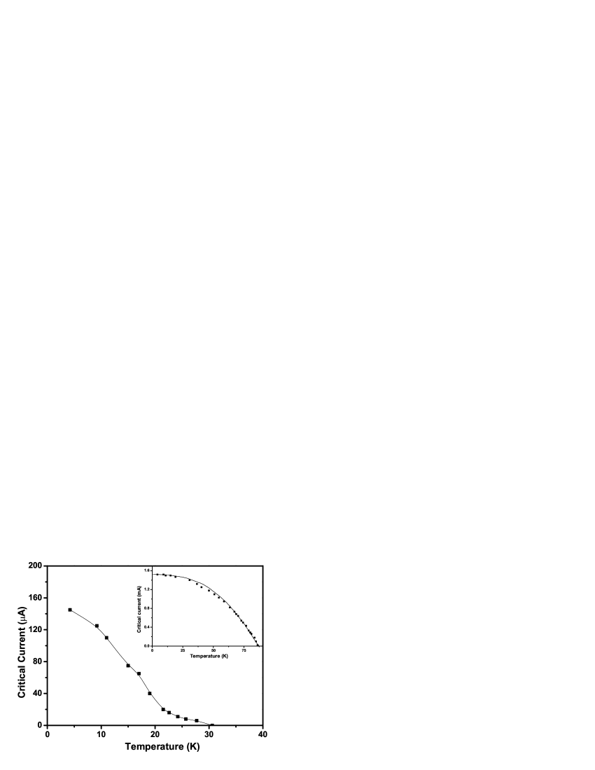
The characteristics of critical current of the surface junction varied with temperature was measured and shown in Fig. 2. As comparison, of conventional IJJ is also shown as the inset of Fig. 2. the solid line in the inset is theoretical calculation of for -axis d/I/d junction by Tanaka etc Tanaka97 . The experimental result is consistent with it. However, the evident deviation was found in the surface d/I/s+d junction. It can be fitted by abnormal temperature dependence instead of when the temperature is close to Tc.
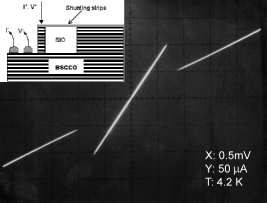
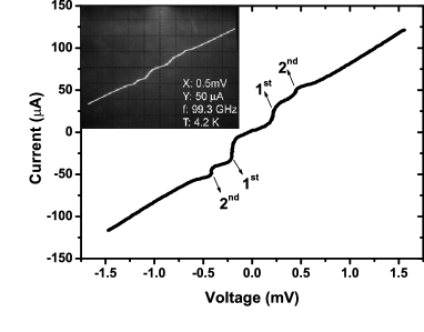
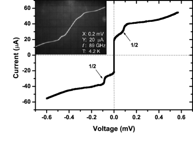
To investigate the detailed feature of the surface d/I/s+d junction, the microwave response was measured. However, with microwave irradiation at GHz and lower frequency, no microwave-induced steps were observed. Because Shapiro steps are only observable when in heavy under-damped Josephson junction Kautz81 ; Wang01a . And the plasma oscillation frequency of the surface junction is estimated to be 100 GHz from , where the critical current density is about 300 A/cm2, the thickness of inter-layer d is 12 Å for BSCCO, and the relative dielectric constant is 3.5 Walkenhorst97 . To observe microwave-induced steps, resistively shunted technology was adopted. It has been well established that Shapiro steps can be observable in resistively shunted IJJ Wang00 ; Wang01b . In this letter, we use a gold stripe to shunt the mesa, the inset of Fig. 3 is the schematic figure of the resistively shunted IJJ. For the critical current of the surface junction is lowest in the stack, the surface junction will be firstly shunted. Detailed discussion of resistively shunting theory was published elsewhere Wang01b . I-V curves shown in Fig. 3 shows typical behavior of RSJ model with a linear contact resistor about in series. The resistance is subtracted in the following figures. With microwave irradiation at 99.3 GHz, the Microwave-induced steps up to second order were observed and shown in Fig. 4. The interval between the first order steps is 410 V, which fits the Josephson voltage-frequency relationship very well. It proves the microwave-induced steps are of the first order supercurrent, which derives from the pair coupling between -wave component in the surface layer and inner -wave layer. Fig. 5 shows the microwave response of the resistively shunted surface junction when the frequency of microwave irradiation changed to 89 GHz. Only two steps were obtained, the interval between them is about 185 V, which fits exactly at . The half-integral steps prove the existence of the second order supercurrent, which originates from the pair coupling between -wave component in the surface layer and -wave in the inner cuprate layer. It is consistent with the prediction of Tanaka Tanaka94 . When the power of microwave source increases, the half-integral steps disappear and conventional Shapiro steps appear. It suggests that the second order supercurrent is more sensitive to microwave irradiation than first order supercurrent derived from -axis pair tunneling between d-wave states. However, because of the low content of -wave states in the mixture s+d states, the microwave induced half-integral steps were concealed by the conventional Shapiro steps with the increase of the microwave power.
In summary, as natural geometry of d/I/s+d junction, the surface junction in intrinsic Josephson junctions stack was measured and discussed. The temperature dependence of critical current shows a significantly difference from the intrinsic d/I/d Josephson junction and follows abnormal temperature dependence when the temperature is close to Tc. With resistively shunting method, the surface junction shows typically RSJ model, the half-integral microwave induced steps were observed as well as conventional integral Shapiro steps, which shows the existence of second order supercurrent and supports strongly Tanaka’s theory.
We thank W. Y. Zhang, J. Li for valuable discussions, H. B. Wang for his technical instruction. This work was supported by the Ministry of Science and Technology of China (Grant No. G19990646), partially carried out at Laboratory of Electronic Intelligent Systems, Research Institute of Electronic Communication, Tohoku University, Japan.
References
- (1) C. C. Tsuei and J. R. Kirtley, Rev. Mod. Phys. 72, 969 (2000)
- (2) J. R. Kirtley et al., Europhys. Lett. 36, 707 (1996)
- (3) R. A. Klemm, C. T. Rieck, and K. Scharnberg, Phys. Rev. B 58, 1051 (1998)
- (4) R. Kleiner et al., Physica C 282, 2435 (1997)
- (5) M. Mössle and R. Kleiner, Phys. Rev. B 59, 4486 (1999)
- (6) J. J. Vicente Alvarez, G. C. Buscaglia, and C. A. Balseiro, Phys. Rev. B 54, 16168 (1996)
- (7) M. Zapotocky, D. L. Maslov, and P. M. Goldbart, Phys. Rev. B 55, 6599 (1997)
- (8) A. M. Martin and J. F. Annett, Phys. Rev. B 57, 8709 (1998)
- (9) J. X. Zhu and C. S. Ting, Phys. Rev. B 57, 3038 (1998)
- (10) Y. Tanaka, Phys. Rev. Lett. 72, 3871 (1994)
- (11) A. G. Sun, D. A. Gajewski, M. B. Maple, and R. C. Dynes, Phys. Rev. Lett. 72, 2267 (1994)
- (12) R. Kleiner et al., Phys. Rev. Lett. 76,(1996) 2161
- (13) J. Lesueur et al., Phys. Rev. B 55 (1997) 3398
- (14) S. I. Woods et al., IEEE Trans, Appl. Supercond. 9, (1999) 3917
- (15) Y. Tanaka and S. Kashiwaya, Phy. Rev. B 56, 892 (1997)
- (16) N. Kim, Y. -J. Doh, H. -S. Chang, and H. -J. Lee, Phys. Rev. B 59, 14639 (1999)
- (17) Y. -J. Doh, H. -J. Lee, and H. -S. Chang, Phys. Rev. B 61 3620 (2000)
- (18) Y. -J. Doh, J. Kim, K. -T. Kim, and H. -J. Lee, Phys. Rev. B 61, R3834 (2000)
- (19) R. L. Kautz, J. Appl. Phys. 52, 3528 (1981)
- (20) H. B. Wang, P. H. Wu, and T. Yamashita, Phys. Rev. Lett. 87, 107002 (2001)
- (21) W. Walkenhorst et al., Phys. Rev. B 56, 8396 (1997)
- (22) H. B. Wang et al., Appl. Phys. Lett. 77, 1017 (2000)
- (23) H. B. Wang et al., Physica C 362, 108 (2001)