Quantum Coherence of Image-Potential States
Abstract
The quantum dynamics of the two-dimensional image-potential states in front of the Cu(100) surface is measured by scanning tunneling microscopy (STM) and spectroscopy (STS). The dispersion relation and the momentum resolved phase-relaxation time of the first image-potential state are determined from the quantum interference patterns in the local density of states (LDOS) at step edges. It is demonstrated that the tip-induced Stark shift does not affect the motion of the electrons parallel to the surface.
pacs:
73.20.At, 68.37.Ef, 72.15.Lh, 72.10.FkThe image-potential states are model states for the study of electronic interactions of electrons at surfaces, a topic that has far reaching consequences for many surface processes. The self interaction of electrons near metallic surfaces gives rise to eigenstates which are confined along the surface normal by the classical image potential on the vacuum side of the crystal surface and by the band structure of the crystal on the other side Echenique78 . The lifetime of electrons injected or excited into an image-potential state is limited mainly by their interaction with bulk electrons. This has been studied in great detail in recent years by energy- and time-resolved two-photon photoemission spectroscopy (2PPE) Hoefer98 ; Hoefer02 ; Fauster99 ; Fauster95 . Theoretical understanding of the involved electron-electron scattering processes has established that the lifetime of image-potential-state electrons is determined by interband scattering with bulk electrons and by intraband contributions Hoefer02 ; Chulkov98 .
The high LDOS of the image-potential states near the surface makes them accessible to STM. They appear at rather high sample bias voltages of . The electric field between tip and sample induces a Stark shift of the eigenenergies to higher values. Interest in image-potential states modified by the presence of an STM tip has focused so far on the fact that the energetic positions of the states are sensitive to the electronic structure of the surface Binnig85 ; Himpsel95 . Spectroscopy of image-potential states by STM has been used to achieve chemical contrast on the nanometer scale for metals on metal surfaces, e.g. Cu on Mo(110) Himpsel95 or Fe/Cr surface alloys Kuk99 .
In this letter, we present for the first time STM measurements of the dynamical properties of the image-potential states in front of the surface. Due to elastic scattering at point defects and step edges of the electrons injected into these states, modulations of the LDOS emerge. Using STS, we determine the energies for the first four image-potential states as well as the dispersion relation and the phase coherence length of the Stark-shifted image-potential state on Cu(100). This opens up the possibility to study these quantities locally in nanostructures. In the case of surface state electrons at metal surfaces the local dynamics has been studied by STS in great detail Li98a ; Buergi99 ; Kliewer00 ; Vitali03 . The results show a good agreement between photoemission and STS experiments on the one side and theory on the other side Kliewer00 ; Vitali03 . A similar comparison is missing in the case of image-potential states.
We used a Cu(100) single crystal sample, carefully prepared by sputtering and annealing cycles in UHV (base pressure ). After cleaning the sample was transferred in situ into a home-built STM operating at . Spectroscopic measurements were performed using a lock-in technique with a modulation of the sample voltage of at a frequency of . All bias voltages are sample potentials measured with respect to the tip.
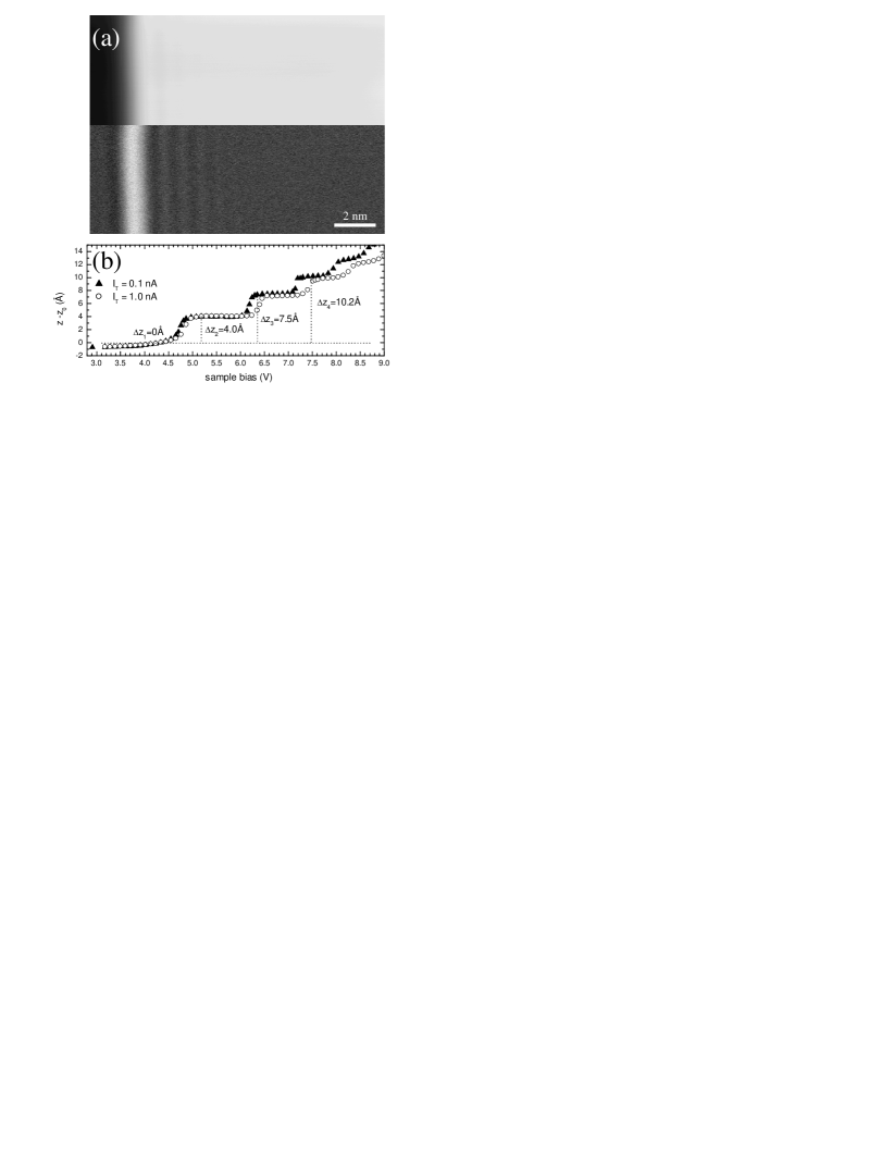
Fig. 1(a) shows a typical STM image of an artificially created step edge. The upper half is a topographic image and the lower half shows the simultaneously acquired -map taken at the same bias voltage. It reveals the quantum interference pattern of the image-potential state created by elastic scattering of the electrons injected by the tip into the image-potential state. Circular standing waves were also observed at point defects. (Not shown here.) We will later present a detailed analysis of these patterns leading to the dispersion relation and the momentum resolved linewidth of the Stark-shifted image-potential state.
The energies of the Stark-shifted image-potential states can be measured using spectroscopy as shown in Fig. 1(b). For this experiment the feedback loop is kept active while sweeping the bias voltage. To maintain a constant current the tip is retracted with increasing bias voltage as more and more states become available to the tunneling electrons. We have taken -spectra at currents of to . The spectra show a series of steps, where each step is due to the contribution of a new image-potential state to the tunneling current allowing us to identify the first four image-potential states. Their energies relative to the vacuum level of the sample are obtained from the bias voltages , at which the steps occur by
| (1) |
where Fauster95 is the work function of Cu(100) and the elementary charge. Note that the states appear above the vacuum level of the substrate but nevertheless they are bound in -direction by the tip and crystal potential respectively. From the absence of any features in below we identify the step at as the state . The energies are considerably larger compared to the unperturbed states which form a Rydberg series below starting at Chulkov99 ; Hoefer02 .
As can be seen from a comparison of the two spectra shown in Fig. 1(b), the states shift to higher energies for higher tunneling currents due to the decreased tip-sample distance. Measurements with different tips, i.e. tips that have been modified by field emission and gentle dipping into the surface, reveal a dependence of the energy levels on the tip properties which is stronger for the higher states. While the state remains at a bias voltage of , we observe the higher states to shift by as much as () and (). This yields a much stronger dependence of the energy levels on tip properties than on tunneling conditions, i.e the current at which the spectroscopy is performed.
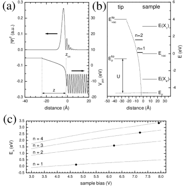
To understand these findings we performed model calculations using a one-dimensional potential as introduced by Chulkov et al. Chulkov99 . This potential reproduces the Rydberg series of the image-potential states and the positions of the projected band edges at the point () in the Cu(100) surface Brillouin zone. We integrated the Schrödinger equation in real space employing the model potential for a 25 layer crystal. The influence of the tip is modelled by adding as function of the bias voltage a linearly increasing potential to the image potential of the crystal reaching from the point (see Ref. Chulkov99, ) to the point where is the tip-sample distance. A similar ansatz has been used in Ref. Limot03, . Since the change in tip-sample distance is given by the plateaus (Fig. 1(b)) we use and treat as the only adjustable parameter in the model assuming equal work functions of tip and sample. This choice was made in favor of discussing the average electric field in the junction Binnig85 since it allows to separate as externally controllable parameter from details of the potential. The model potential and the probability distribution of the resulting wave function are shown in Fig. 2(a). Fig 2(b) shows schematically the resulting energy level diagram. In such a simple model, the energies of the image-potential states in the electric field of the STM tip are reproduced for all observed. This is shown in Fig. 2(c), where the calculated energies are plotted as a function of the applied bias voltage for corresponding to the measurement with a tunneling current of . The agreement is excellent. To reproduce the energy levels for the measurement at a current of a is found. We emphasize that there is no need for an n-dependent ”surface-corrugation parameter” as was employed earlier Binnig85 . To arrive at the expected smaller values of to Gim87 one has to improve the treatment of the tip electrode. The detailed inclusion of the image potential at the surface of the tip in a calculation using two Cu(100) model potentials facing each other yielded values which were lower than the ones found above. On the other hand, the radius of curvature of the tip can be neglected. Only for unrealistically sharp tips with the potential near the tip will fall off appreciably more quickly than the linear potential. We conclude that to explain the variation of the with different tips the contact potential and not the tip radius is the decisive quantity. From the experimental point of view it is quite likely that the tungsten tip is coated with copper, since it is frequently prepared by slightly dipping it into the surface. Both, the composition and the morphology of the very end of the tip can lead to a lower work function compared to that of the Cu(100) surface, which can be compensated by a reduced .
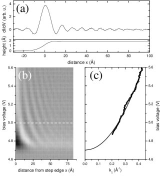
In the following, the dynamics of the the image-potential-state electrons in front of the surface will be discussed in detail. Due to elastic scattering of these electrons at point defects and step edges, modulations of the LDOS are created through quantum interference (Fig. 1(a) and Fig. 3(a)). This allows to study the dynamics of the states with non-vanishing momentum parallel to the surface locally. The analysis of the interference pattern of electrons scattered at a step edge enables the determination of their wave vector and phase coherence length as a function of energy. The interference pattern is measured through the signal which is proportional to the LDOS at the given energy. In Fig. 3(b) is measured for bias voltages ranging from to at increasing distances from the step edge. The resulting curves are represented as a grey scale map, where horizontal line sections are the energy resolved electron density oscillations as shown in Fig. 3(a). The density oscillations reveal the parabolic dispersion relation of the state with and (Fig 3(c)). However, with the help of the calculations presented above, the influence of the tip on the dispersion of the image-potential state can be corrected for. Since the data are collected in open feedback mode, i.e. the distance between tip and sample is kept constant, one needs only to compensate for the shift of the energy at with changing electric field during the bias voltage sweep. The dependence of the state’s energy on the applied bias voltage close to is approximately linear. From the calculations shown in Fig. 2(c) we get . Using this correction, we obtain an effective mass of . This agrees perfectly with the effective mass of the image-potential state as determined by 2PPE Fauster95 . Similarly we find an effective mass of the state of . An increase in the effective mass for was also observed by 2PPE Weinelt02 .
The standing wave pattern decays with increasing distance from the step edge due to geometric factors and to a loss of coherence Buergi99 . The decaying LDOS pattern formed by the image-potential states near a step edge can be described by
| (2) |
where is an overall proportionality constant, the reflectivity of the step edge, the phase coherence length, the wave vector of the electron parallel to the surface plane, and the Bessel function of zeroth order.
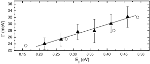
To determine the lifetime of an electron in the image-potential state we have analyzed quantitatively the quantum interference pattern and measured the phase coherence length as a function of energy on large defect free terraces. The scattering processes thus studied are those experienced in the absence of any defects Buergi99 ; Vitali03 . Inelastic scattering at the step edge leads to a reduced overall amplitude of the standing waves described by in Eq. 2. Care was taken to account for instrumental broadening through the applied bias modulation when measuring the signal which also induces a decay of the wave pattern Buergi99 . The obtained phase coherence lengths of are converted into linewidths through by using the measured and according to the dispersion relation (Fig. 3). The results shown in Fig. 4 agree excellently with the -resolved linewidths found by 2PPE measurements Hoefer02 . In agreement with theory, we find to increase linearly with energy, although the rate of obtained from the fit in Fig. 4 is lower than the theoretical prediction Hoefer02 . The comparison of our results with the 2PPE measurements demonstrates that the presence of the tip does not alter substantially the dynamical properties of electrons in the image-potential states. Although the state shifts by as much as due to the presence of the electric field, it is still located near the center of the wide directional band gap of Cu(100). There is thus no significant change in the coupling to the bulk electrons, which is the main contribution to the linewidth.
In conclusion, we observed for the first time density modulations of image-potential-state electrons in the vicinity of steps and point defects on Cu(100). The quantum interference patterns allow us to determine the dispersion relation of the states which experience a Stark shift due to the electric field in the tunneling junction. Furthermore we measured the phase coherence length of the electrons on clean terraces. Both, the dispersion relation and the phase coherence length agree well with the results of non-local photoemission experiments. This shows that the motion of the electrons parallel to the surface is not noticeably affected by the field of the STM tip. Due to the local character of the measurement the STM can therefore be used to study the dynamical behavior of image-potential-state electrons confined laterally to nanostructures and to characterize the scattering properties of surface defects and adsorbates.
References
- (1) P.M. Echenique and J.B. Pendry, J. Phys. C 11, 2065 (1978).
- (2) U. Höfer et al., Science 277, 1480 (1997).
- (3) W. Berthold et al., Phys. Rev. Lett. 88, 056805 (2002).
- (4) Ch. Reuß et al., Phys. Rev. Lett. 82, 153 (1999).
- (5) Th. Fauster and W. Steinmann, in Photonic Probes of Surfaces, edited by P. Halevi (North Holland, Amsterdam, 1995), pp. 347-411.
- (6) E. V. Chulkov et al., Phys. Rev. Lett. 80, 4947 (1998).
- (7) G. Binnig et al., Phys. Rev. Lett. 55, 991 (1985).
- (8) T. Jung, Y. W. Mo, and F. J. Himpsel, Phys. Rev. Lett. 74, 1641 (1995).
- (9) Y.J. Choi et al., Phys. Rev. B 59, 10918 (1999).
- (10) J. Li et al., Phys. Rev. Lett. 81, 4464 (1998).
- (11) L. Bürgi, O. Jeandupeux, H. Brune, and K. Kern, Phys. Rev. Lett. 82, 4516 (1999).
- (12) J. Kliewer et al., Science 288, 1399 (2000).
- (13) L. Vitali et al., Surf. Sci. 523, L47 (2003).
- (14) E.V. Chulkov, V.M. Silkin, P.M. Echenique, Surf. Sci. 437, 330 (1999).
- (15) L. Limot et al., cond-mat/0301568 (unpublished).
- (16) J.K. Gimzewski and R. Möller, Phys. Rev. B 36, 1284 (1987).
- (17) To enhance the contrast, the average value of each horizontal line has been subtracted.
- (18) M. Weinelt, J. Phys.: Condens. Matter 14, R1099 (2002)