Influence of impurity-scattering on tunneling conductance in d-wave superconductors with broken time reversal symmetry
Abstract
Effects of impurity scattering on tunneling conductance in dirty normal-metal/insulator/superconductor junctions are studied based on the Kubo formula and the recursive Green function method. The zero-bias conductance peak (ZBCP) is a consequence of the unconventional pairing symmetry in superconductors. The impurity scattering in normal metals suppresses the amplitude of the ZBCP. The degree of the suppression agrees well with results of the quasiclassical Green function theory. When superconductors have -wave pairing symmetry, the time-reversal symmetry is broken in superconductors and the ZBCP splits into two peaks. The random impurity scattering reduces the height of the two splitting peaks. The position of the splitting peaks, however, almost remains unchanged even in the presence of the strong impurity scattering. Thus the two splitting peaks never merge into a single ZBCP.
1 Introduction
Charge transport in unconventional superconductors shows remarkable properties which cannot be expected in conventional -wave superconductors. One of the striking effects is the zero-bias conductance peak (ZBCP) in normal-metal/unconventional superconductor junctions[1]. In hybrid structures consisting of high-TC superconductors, a number of experiments observed the ZBCP [7, 8, 2, 3, 4, 5, 6, 9, 10]. The zero-energy state (ZES) [11] formed at a surface of the unconventional superconductor is responsible for the ZBCP [1]. The interference effect of a quasiparticle in the presence of the sign-change in the pair potential is the origin of the ZES [12, 13, 14, 15, 16, 17, 18]. The ZES is also responsible for the low-temperature anomaly of the Josephson current in unconventional superconductor junctions [19, 20, 21, 22, 23, 24, 25] and anomalies of the charge transport in ferromagnet/unconventional superconductor junctions [26, 27, 28, 29, 30, 31].
Since the ZES is a result of the interference effect of a quasiparticle, it is sensitive to the time-reversal symmetry (TRS) of systems. Actually it has been confirmed in normal-metal/-wave superconductor junctions that the ZBCP splits into two peaks by applying magnetic fields [32, 33, 34, 35]. It has been also pointed out that the ZBCP splits into two peaks when the TRS is broken in superconductors [32, 36, 37, 38, 39, 40]. Theories showed a possibility of - [41] or [42]-wave broken time-reversal symmetry states (BTRSS) at surfaces of superconductors. If such BTRSS’s are stable at the surface of superconductors, they may bring significant influences on transport properties [43, 44]. Experimental results, however, are still controversial. Some experiments reported the split of the ZBCP in the absence of magnetic field [45, 46, 47, 48],others did not show the zero-field splitting even in low temperatures [49, 2, 5, 3, 9, 50]. Moreover a experiment of the Josephson junctions concluded the absence of the BTRSS at interfaces of -wave junctions [51]. Thus it is very important to theoretically address the origin of the splitting. There are several factors which determine the magnitude of splitting of the ZBCP: the transmission probability of the junctions [39], the roughness of the interface [52], the impurity scattering in superconductors [53] and the impurity scattering in normal metals. Among them, effects of the impurity scattering in normal metals has not been studied yet. We note that effects of random potentials on the split of the ZBCP are also unclear within theoretical studies at present. Some theories based on the quasiclassical Green function method [54, 55, 56, 57] did not show the splitting [58, 59, 60, 61, 62, 63], whereas others concluded the split of the ZBCP by a numerical simulation [52] and an analytic calculation [53]. When the BTRSS is formed at the NS interface, a group of experiment predicted that the two splitting peaks may merge into a single ZBCP by the impurity scattering [64].
In dirty normal-metal/insulator/superconductor (DN/I/S) junctions, there are many theoretical studies (see a review [65]) on conventional -wave superconductor junctions such as numerical methods [66, 67, 68], the random matrix theory [65, 69, 70] and the quasiclassical Green function approach [71, 72, 73, 74, 75, 76, 77]. These studies show a wide variety in line shapes of the conductance depending on the Thouless energy and the resistance of DN. In particular, the ZBCP is an important conclusion in the low transparent junctions even in the -wave junctions. We note that the interference of a quasiparticle while traveling the diffusive metals causes the ZBCP in the -wave junctions. Recently, the full resistance () of the disordered junctions is derived from a microscopic theory [78]. By applying this theory to -wave junctions, we show various transport properties which reflect the unconventional pairing symmetry in superconductors. When the axis of high- superconductors is oriented 45 degrees from the interface normal, at the zero temperature can be expressed as [78], where is the resistance of a diffusive metal and is the resistance of a clean junction. The resistance of the disordered junction is given by the simple summation of the two resistance, which indicates the absence of the proximity effect [79, 80, 81]. At the present stage, however, there is no corresponding studies in DN/I/-wave superconductor junctions with the BTRSS.
In this paper, effects of the randomness on the ZBCP in DN/I/S junctions are studied numerically by using the recursive Green function method. We mainly consider the -wave pairing symmetry in superconductors. For comparison, we also discuss the conductance in the - and -wave junctions which are the two limitting cases of the -wave junctions. First we confirm the proximity effect in -wave junctions. The total resistance at the zero-bias in disordered -wave junctions shows the reentrant behavior as a function of , which is consistent with the quasiclassical theory. We also confirm that the resistance in disordered -wave junctions increases monotonically with the increase of [82, 83] since there is no proximity effect. The calculated results are consistent with the quasiclassical theory [78]. In -wave junctions, we show that the proximity effect appears when -wave component becomes dominant. In junctions, the ZBCP splits into two peaks because of the BTRSS and the impurity scattering reduces the height of the splitting peaks. The two splitting peaks, however, do not merge into a single peak. In the light of our theory, the single sharp ZBCP observed in experiments [2, 3, 5] is a strong evidence for the formation of the pure -wave symmetry state at the interface.
This paper is organized as follows. In Sec. II, the model and method are presented. The numerical results are shown in Sec. III. In Sec. IV, we summarize this paper.
2 Model and Method
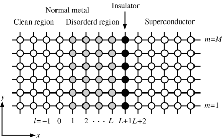
Let us consider a normal-metal / superconductor junction on the two-dimensional tight-binding model as shown in Fig. 1, where labels a lattice site. We assume the periodic boundary condition in the direction and the width of the junction is , where is the lattice constant. The BCS Hamiltonian of the system is expressed as,
| (1) |
where () is the creation (annihilation) operator of an electron at with spin or and is the Fermi energy. The summation runs over nearest neighbor sites and is the nearest neighbor hopping-integral. We assume that the on-site potential is zero far from the interface in the normal metal and in the superconductor, (i.e., for and ). In the disordered region, , the potential is given by random number uniformly distributed in the range of
| (2) |
The insulating barrier is described by the potential for all . When a superconductor has the -wave pairing symmetry, the pair potential is given by
| (3) |
When the axis of a high- superconductor is oriented by 45 degrees from the interface normal, the pair potential is given by
| (4) |
We note that the tight-binding lattices do not correspond to the two-dimensional CuO2 plane in high- superconductors. The tight-binding model represents the two-dimensional space. In our model, we introduce the pair potential between the next nearest neighbor sites to describe junctions under consideration. An alternative way is keeping the pair potential between the nearest neighbor sites and rotating the square lattice by 45 degrees. There are no essential differences between results in the two models when we focus on the formation of the ZES. This is because the ZES is a consequence of the -wave symmetry of the pair potential. The BTRSS is characterized by the -wave symmetry and the pair potential is described by
| (5) |
where is a parameter which characterizes the degree of the time-reversal symmetry breaking. When -wave component appears only at a surface of a superconductor, we describe the pair potential as
| (6) |
where is comparable to the coherence length of -wave superconductors [39, 41]. In a normal metal, the pair potential is taken to be zero.
The BCS Hamiltonian in Eq. (1) can be diagonalized by applying the Bogoliubov transformation,
| (7) |
where () is creation (annihilation) operator of a Bogoliubov quasiparticle. We omit the spin index of the wavefunction () since we do not consider the spin-dependent potential. In this way, the Bogoliubov-de Gennes (BdG) equation is derived on the tight-binding lattice. We solve the BdG equation by using the recursive Green function method [84, 79]. The Green function is defined in a matrix form
| (8) |
where is the eigen value of the BdG equation, is the vector with components and -th (-th) component is (). The differential conductance of the junction is calculated to be
| (9) |
with , where is the bais voltage applied to the NS junction [82, 85]. When is a matrix, means the summation of . The conductance in this method is identical to that in the well known conductance formula [86, 87]. By averaging over different configuration of randomness, the mean value of conductance is obtained. The conductance in normal conductors can be also calculated in the conventional recursive Green function method [84]. The advantage of the method is wide applicability to various systems such as, the clean (ballistic) junctions, the dirty (diffusive) junctions and the junctions in the localization regime [88].
3 Results
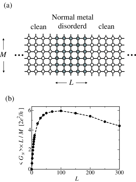
Throughout this paper, we fix the Fermi energy at , the amplitude of the pair potential in the -wave component at and the impurity potential at . In order to determine the mean free path at the Fermi energy, we first calculate the normal conductance as a function of the length of the disordered region in Fig. 2(b). The ensemble average is carried out over 500 samples with different random impurity configurations. When is small, . Thus the disordered region is in the quasiballistic transport regime and is proportional to as shown in . In the diffusive regime, coincides with the conductivity which is independent of sample size. Thus in Fig 2(b) corresponds to the diffusive regime and the mean free path is estimated to be about 6 . For large , the disordered region is in the localization transport regime and the conductance decreases with in proportional to , where is the localization length of an electron.
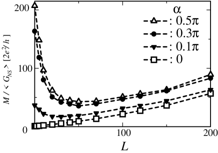
In Fig. 3, we show the resistance at the zero-bias in DN/I/S junctions as a function of . We assume pairing symmetry in superconductors as shown in Eq. (5), where . The results for correspond to the resistance in -wave junctions. The resistance for first decreases with the increase of . Cooper pairs penetrate into normal metals and have a finite amplitude. This is a source of the proximity effect. As a consequence, the reflectionless tunneling suppresses the resistance at the zero-bias. For large , the resistance increases linearly with . The reentrant behavior of the resistance for is the direct consequence of the proximity effect. The results for correspond to the resistance in -wave functions. The resistance does not show the reentrant behavior and increases almost linearly with the increase of . In this case, the proximity effect is absent. The amplitude of the Cooper pairs becomes almost zero because the contribution of the pair potential with positive sign and that with negative sign cancel out with each other. For , the proximity effect appears because of the -wave component in the pair potential and the resistance show the weak reentrant behavior as a function of . For , the reentrant behavior becomes rather remarkable and the results are close to those in the -wave junctions. According to the quasiclassical Green function theory, the resistance of the -wave junctions can be simply given by
| (10) |
where is the resistance in DN and is the resistance of the clean junction. The summation of these two resistance gives the full resistance of the disordered junctions because there is no proximity effect. The absence of the proximity effect is responsible for the anomaly in the Josephson current through diffusive metals [80, 81].
In Fig. 4, we show the conductance in clean N/I/S junctions as a function of the applied bias voltage, where and . For , junctions become -wave junctions and the conductance has two peaks at which reflect the singularity of the density of states in -wave superconductors. Junctions with correspond to -wave junctions and the results show the ZBCP owing to the ZES at the junction interface. For , the ZBCP splits into two peaks because the TRS is broken by the -wave component in the pair potential [32]. The degree of the splitting increases with increasing . The calculated results basically remain unchanged when we assume the -wave component only at the interface. Since the splitting was observed in several experiments [45, 46, 47, 48], the zero-field splitting of the ZBCP has been believed to be an evidence of the BTRSS. On the other hand, other experiment [49, 2, 5, 3, 9, 50] did not show the zero-field splitting. Thus the experimental results are still controversial at present. There are some reasons which explain the contradiction in experiments. One of them is the sample quality of the junction. Actually a group of experiment insists that the zero-field split would be found when the sample quality is good enough and the measurement is done in sufficiently low temperatures. If this prediction is true, the impurity scattering might unify the splitting peaks. We try to check this prediction as follows.
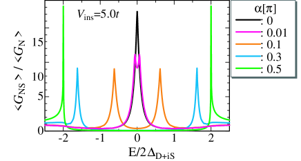
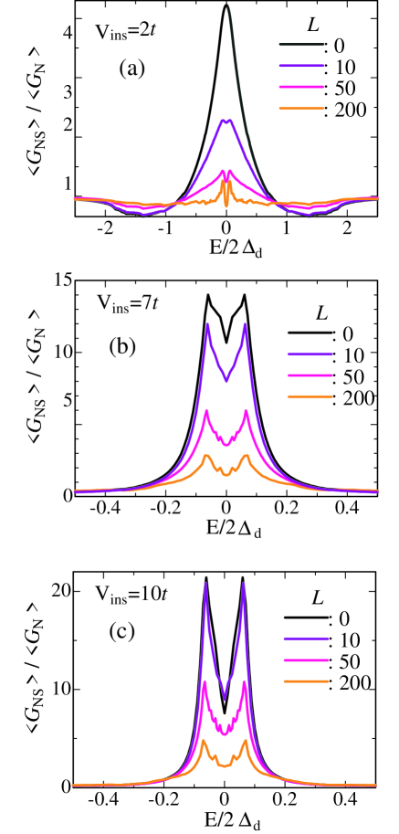
We introduce the impurity potential in normal metals of -wave junctions. In Fig. 5, the conductance is plotted as a function of the bias voltage for several , where = 2, 7 and 10 in (a), (b) and (c), respectively. The -wave component is introduced only at the NS interface and in Eq. (6) is chosen to be lattice constants. The amplitude of the -wave pair potential is fixed at . When the transparency of the interface is high, the ZBCP in clean junctions does not split into two peaks even in the presence of the -wave component as shown in (a). The splitting can be seen in the disordered junctions as shown in the results for finite . Thus the impurity scattering in normal metal seems to assist the splitting of the ZBCP. At the same time, the amplitude of the conductance decreases with increasing . In highly transparent junctions, the calculated results indicate the opposite conclusion to the experimental prediction. When the transparency of the junction becomes low, the ZBCP splits into two even in clean junctions as show in (b) and (c). The amplitude of the conductance decreases with the increase of the resistance of normal metals as well as those in (a). It is important that the degree of the splitting are not changed by the impurity scattering. In low transparent junctions, our results are also contradict to the experimental prediction. We conclude that the impurity scattering in low transparent junctions does not merge the splitting peaks into a single ZBCP.
4 Conclusions
We numerically calculated the differential conductance in dirty normal metal/ insulator/ superconductor junctions by using the recursive Green function method. In superconductors, we assumed pairing symmetry which breaks the time-reversal symmetry of the junctions. In pure -wave (pure -wave) junctions, we confirmed the presence (absence) of the proximity effect, which agrees with the quasiclassical Green function theory. In the case of the symmetry, the proximity effect recovers when the pair amplitude of the -wave symmetry becomes dominant. In highly transparent clean junctions, we found the single ZBCP even in the absence of the time-reversal symmetry [39]. The ZBCP, however, splits into two peaks owing to the impurity scattering. The -wave component splits the zero-bias conductance peak into two peaks in low transparent junctions even in the clean limit. The amplitudes of the splitting peaks decreases with the increase of the impurity scattering in normal metals. The peak position, however, remains unchanged even in the presence of the strong impurity scattering. Thus we conclude that the impurity scattering does not merge the two splitting peaks.
Acknowledgements.
This work was partially supported by the Core Research for Evolutional Science and Technology (CREST) of the Japan Science and Technology Corporation (JST). The computational aspect of this work has been performed at the facilities of the Superconputer Center, Institute of Solid State Physics, University of Tokyo and the Computer Center. J.I. acknowledges support by the NEDO international Joint Research project ”Nano-scale Magnetoelectronics”.References
- [1] Y. Tanaka and S. Kashiwaya: Phys. Rev. Lett. 74 (1995) 3451.
- [2] L. Alff, H. Takashima, S. Kashiwaya, N. Terada, H. Ihara, Y. Tanaka, M. Koyanagi and K. Kajimura: Phys. Rev. B 55 (1997) 14757.
- [3] J. Y. T. Wei, N.-C. Yeh, D. F. Garrigus and M. Strasik: Phys. Rev. Lett. 81 (1998) 2542.
- [4] W. Wang, M. Yamazaki, K. Lee and I. Iguchi: Phys. Rev. B 60 (1999) 4272.
- [5] I. Iguchi, W. Wang, M. Yamazaki, Y. Tanaka, and S. Kashiwaya: Phys. Rev. B 62 (2000) R6131.
- [6] S. Kashiwaya and Y. Tanaka: Rep. Prog. Phys. 63 (2000) 1641.
- [7] S. Kashiwaya, Y. Tanaka, M. Koyanagi, H. Takashima and K. Kajimura: Phys. Rev. B 51 (1995) 1350.
- [8] S. Kashiwaya, Y. Tanaka, M. Koyanagi and K. Kajimura: Phys. Rev. B 53 (1996) 2667.
- [9] A. Sawa, S. Kashiwaya, H. Obara, H. Yamasaki, M. Koyanagi, Y. Tanaka and N. Yoshida: Physica C 339 (2000) 107.
- [10] H. Kashiwaya, A. Sawa, S. Kashiwaya, H. Yamazaki, M. Koyanagi, I. Kurosawa, Y. Tanaka, and I. Iguchi: Physica C 357-360 (2001) 1610.
- [11] C. R. Hu: Phys. Rev. Lett. 72 (1994) 1526.
- [12] M. Matsumoto and H. Shiba, J. Phys. Soc. Jpn. 64 (1995) 1703.
- [13] Y. Nagato and K. Nagai, Phys. Rev. B 51 (1995) 16254.
- [14] Y. Ohashi, J. Phys. Soc. Jpn. 65 (1996) 823; Y. Ohashi and S. Takada, J. Phys. Soc. Jpn. 65 (1996) 246.
- [15] Y. Tanuma, Y. Tanaka, M. Yamashiro and S. Kashiwaya : Phys. Rev. B 57 (1998) 7997; Y. Tanuma, Y. Tanaka, K. Kuroki and S. Kashiwaya: Phys. Rev. B 64 (2001) 214510; Y. Tanuma, K. Kuroki Y. Tanaka, R. Arita, S. Kashiwaya and H. Aoki: Phys. Rev. B 66 (2002) 094507; Y. Tanuma, K. Kuroki Y. Tanaka, and S. Kashiwaya: Phys. Rev. B 66 (2002) 174502.
- [16] M. Yamashiro, Y. Tanaka and S. Kashiwaya: Phys. Rev. B 56 (1997) 7847; M. Yamashiro, Y. Tanaka Y. Tanuma and S. Kashiwaya: J. Phys. Soc. Jpn. 68 (1999) 2019; M. Yamashiro, Y. Tanaka N. Yoshida and S. Kashiwaya: J. Phys. Soc. Jpn. 67 (1998) 3224.
- [17] Y. Tanaka, H. Tsuchiura, Y. Tanuma and S. Kashiwaya: J. Phys. Soc. Jpn. 71 (2002) 271; Y. Tanaka, Y. Tanuma K. Kuroki and S. Kashiwaya: J. Phys. Soc. Jpn. 71 (2002) 2102.
- [18] H.X. Tang, Jian-Xin Zhu and Z.D. Wang: Phys. Rev. B 54 (1996) 12509; Jian-Xin Zhu H. X. Tang and Z.D. Wang: Phys. Rev. B 54 (1996) 7354.
- [19] Y. Tanaka: Phys. Rev. Lett. 72 (1994) 3871; Y. Tanaka and S. Kashiwaya: Phys. Rev. B 53 (1996) 11957; Phys. Rev. B 56 (1997) 892; Phys. Rev. B 58 (1998) R2948.
- [20] Y. S. Barash, H. Burkhardt and D. Rainer, Phys. Rev. Lett. 77 (1996) 4070.
- [21] Y. Tanaka and S. Kashiwaya: J. Phys. Soc. Jpn. 68 (1999) 3485; J. Phys. Soc. Jpn. 69 (2000) 1152.
- [22] Y. Tanaka, T. Hirai, K. Kusakabe and S. Kashiwaya: Phys. Rev. B 60 (1999) 6308; T. Hirai, K. Kusakabe and Y. Tanaka Physica C 336 (2000) 107; K. Kusakabe and Y. Tanaka; Physica C 367 (2002) 123; K. Kusakabe and Y. Tanaka; J. Phys. Chem. Solids 63 (2002) 1511.
- [23] Y. Asano: Phys. Rev. B 64 (2001) 224515.
- [24] Y. Asano and K. Katabuchi: J. Phys. Soc. Jpn. 71 (2002) 1974.
- [25] Y. Asano, Y. Tanaka, M. Sigrist and S. Kashiwaya: cond-mat/0212353.
- [26] J-X. Zhu, B. Friedman, and C. S. Ting: Phys. Rev. B 59 (1999) 9558.
- [27] S. Kashiwaya et al.: Phys. Rev. B 60 (1999) 3527.
- [28] I. Zutic and O. T. Valls: Phys. Rev. B 60 (1999) 6320.
- [29] N. Yoshida, Y. Tanaka, J. Inoue, and S. Kashiwaya: J. Phys. Soc. Jpn. 68 (1999) 1071.
- [30] T. Hirai, N. Yoshida, Y. Tanaka, J. Inoue and S. Kashiwaya: J. Phys. Soc. Jpn. 70 (2001) 1885.
- [31] N. Yoshida, H. Itoh, T. Hirai, Y. Tanaka, J. Inoue and S. Kashiwaya: Phsica C 367 (2002) 135.
- [32] M. Fogelström, D. Rainer, and J. A. Sauls: Phys. Rev. Lett. 79 (1997) 281; D. Rainer, H. Burkhardt, M. Fogelström, and J. A. Sauls: J. Phys. Chem. Solids 59 (1998) 2040.
- [33] Y. Tanaka, H. Tsuchiura, Y. Tanuma and S. Kashiwaya: J. Phys. Soc. Jpn. 71 (2002) 271.
- [34] Y. Tanaka, H. Itoh, H. Tsuchiura, Y. Tanuma, J. Inoue, and S. Kashiwya: J. Phys. Soc. Jpn. 71 (2002) 2005.
- [35] Y. Tanaka, Y. Tanuma, K. Kuroki and S. Kashiwaya: J. Phys. Soc. Jpn. 71 (2002) 2102.
- [36] S. Kashiwaya, Y. Tanaka, M. Koyanagi and K. Kjimura, J. Phys. Chem. Solids 56 (1995) 1721.
- [37] Y. Tanuma, Y. Tanaka, M. Ogata and S. Kashiwaya: J. Phys. Soc. Jpn., 67 (1998) 1118.
- [38] Y. Tanuma, Y. Tanaka, M. Ogata and S. Kashiwaya: Phys. Rev. B 60 (1999) 9817.
- [39] Y. Tanuma, Y. Tanaka, and S. Kashiwaya: Rhys. Rev. B 64 (2001) 214519.
- [40] Jian-Xin Zhu, B. Friedman and C.S. Ting: Phys. Rev. B 59 (1999) 3353; Jian-Xin Zhu and C.S. Ting: Phys. Rev. B 60 (1999) R3739; Jian-Xin Zhu and C.S. Ting: Phys. Rev. B 57 (1998) 3038.
- [41] M. Matsumoto and H. Shiba: J. Phys. Soc. Jpn. 64 (1995) 3384; J. Phys. Soc. Jpn. 64 (1995) 4867.
- [42] R. B. Laughlin: Phys. Rev. Lett. 80 (1998) 5188.
- [43] Y. Tanaka, Y. Tanuma, and S. Kashiwaya: Phys. Rev. B 64 (2001) 054510.
- [44] Y. Tanaka, T. Asai, N. Yoshida, J. Inoue and S. Kashiwaya: Phys. Rev. B 61 (2000) R11902.
- [45] M. Covington, M. Aprili, E. Paraoanu, L. H. Greene, F. Xu, J. Zhu, and C. A. Mirkin: Phys. Rev. Lett. 79 (1997) 277; M. Aprili, E. Badica and L. H. Greene Phys. Rev. Lett. 83 (1999) 4630.
- [46] A. Biswas, P. Fournier, M. M. Qazilbash, V. N. Smolyaninova, H. Balci, and R. L. Greene: Phys. Rev. Lett. 88 (2002) 207004.
- [47] Y. Dagan and G. Deutscher: Phys. Rev. Lett. 87 (2001) 177004.
- [48] A. Sharoni, O. Millo, A. Kohen, Y. Dagan, R. Beck, G. Deutscher, and G. Koren: Phys. Rev. B 65 (2002) 134526.
- [49] J. W. Ekin, Y. Xu, S. Mao, T. Venkatesan, D. W. Face, M. Eddy, and S. A. Wolf: Phys. Rev. B 56 (1997) 13746.
- [50] H. Aubin, L. H. Greene, Sha Jian and D. G. Hinks: Phys. Rev. Lett. 89 (2002) 177001.
- [51] W. K. Neils and D. J. Van Harlingen: Phys. Rev. Lett. 88 (2002) 047001.
- [52] Y. Asano and Y. Tanaka: Phys. Rev. B 65 (2002) 064522.
- [53] Y. Asano, Y. Tanaka and S. Kashiwaya: cond-mat/0302287.
- [54] G. Eilenberger: Z. Phys. 214 (1968) 195.
- [55] A. I. Larkin and Yu. N. Ovchinikov: Eksp. Teor. Fiz. 55 (1968) 2262.[Sov. Phys. JETP 28 (1968) 1200.]
- [56] A. V. Zaitsev: Zh. Eksp. Teor. Fiz. 86 (1984) 1742. [Sov. Phys. JETP 59 (1984) 1015.]
- [57] A. L. Schelankov: J. Low. Tem. Phys. 60 (1985) 29.
- [58] C. Bruder: Phys. Rev. B 41 (1990) 4017.
- [59] Y. S. Barash, A. A. Svidzinsky and H. Burkhardt: Phys. Rev. B 55 (1997) 15282.
- [60] A. A. Golubov, M. Y. Kupriyanov: Pis’ma Zh. Eksp. Teor. fiz 69 (1999) 242.[ Sov. Phys. JETP Lett. 69 (1999) 262.]; 67 (1998) 478.[ Sov. Phys. JETP Lett. 67 (1998) 501.]
- [61] A. Poenicke, Yu. S. Barash, C. Bruder, and V. Istyukov: Phys. Rev. B 59 (1999) 7102.
- [62] K. Yamada, Y. Nagato, S. Higashitani and K. Nagai: J. Phys. Soc. Jpn. 65 (1996) 1540.
- [63] T. Lück, U. Eckern, and A. Shelankov: Phys. Rev. B 63 (2002) 064510.
- [64] Discussion at M2S 2002.
- [65] C. W. J. Beenakker: Rev. Mod. Phys. 69 (1997) 731.
- [66] C. J. Lambert: J. Phys. Condens. Matter 3 (1991) 6579.
- [67] Y. Takane and H. Ebisawa: J. Phys. Soc. Jpn. 61 (1992) 2858.
- [68] G. B. Lesovik, A. L. Fauchere, and G. Blatter: Phys. Rev. B 55 (1997) 3146.
- [69] C. W. J. Beenakker: Phys. Rev. B 46 (1992) 12841.
- [70] C. W. J. Beenakker, B. Rejaei and J. A. Melsen: Phys. Rev. Lett. 72 (1994) 2470.
- [71] A. F. Volkov, A. V. Zaitsev and T. M. Klapwijk: Physica C 210 (1993) 21.
- [72] S. Yip: Phys. Rev. B 52 (1995) 3087.
- [73] A. A. Golubov, F. K. Wilhelm, and A. D. Zaikin: Phys. Rev. B 55 (1997) 1123.
- [74] A. F. Volkov and H. Takayanagi: Phys. Rev. B 56 (1997) 11184.
- [75] Yu. V. Nazarov: Phys. Rev. Lett. 73 (1994) 1420.
- [76] Yu. V. Nazarov: Superlatt. Microstruct. 25 (1999) 1221; cond-mat/9811155.
- [77] Y. Tanaka, A. Golubov and S. Kashiwaya: Phys. Rev. B 2003 in press.
- [78] Y. Tanaka, Yu. V. Nazarov and S. Kashiwaya: cond-mat/0208009.
- [79] Y. Asano: Phys. Rev. B 63 (2001) 052512.
- [80] Y. Asano: Phys. Rev. B 64 (2001) 014511.
- [81] Y. Asano: J Phys. Soc. Jpn. 71 (2002) 905.
- [82] H. Itoh, Y. Tanaka, J. Inoue, and S. Kashiwaya: Physica C 367 (2002) 99; N. Yoshida, Y. Asano, H. Itoh, Y. Tanaka, J. Inoue and S. Kashiwaya J. Phys. Soc. Jpn. 72 No. 4 (2003)
- [83] H. Itoh, N. Kiraura, Y. Yoshida, Y. Tanaka, J. Inoue, Y. Asano and S. Kashiwaya: ”Toward the Controllable Qunatum States”, Eds. H. Takayanagi and J. Nitta, pp. 173, World Scientific Publishing (2003).
- [84] P. A. Lee and D. S. Fisher: Phys. Rev. Lett. 47 (1981) 882.
- [85] R. Kubo: J. Phys. Soc. Jpn. 12 (1957) 570.
- [86] G. E. Blonder, M. Tinkham and T. M. Klapwijk: Phys. Rev. B 25 (1982) 4515.
- [87] Y. Takane and H. Ebisawa: J. Phys. Soc. Jpn. 61 (1992) 1685.
- [88] Y. Asano: Phys. Rev. B 66 (2002) 174506.