Also at ]London Centre for Nanotechnology, Gordon St, London WC1E 6BT
Also at ]London Centre for Nanotechnology, Gordon St, London WC1E 6BT
Soliton effects in dangling-bond wires on Si(001)
Abstract
Dangling bond wires on Si(001) are prototypical one dimensional wires, which are expected to show polaronic and solitonic effects. We present electronic structure calculations, using the tight binding model, of solitons in dangling-bond wires, and demonstrate that these defects are stable in even-length wires, although approximately 0.1 eV higher in energy than a perfect wire. We also note that in contrast to conjugated polymer systems, there are two types of soliton and that the type of soliton has strong effects on the energetics of the bandgap edges, with formation of intra-gap states between 0.1 eV and 0.2 eV from the band edges. These intra-gap states are localised on the atoms comprising the soliton.
pacs:
68.65.+k; 73.20.-r; 71.15.Nc; 71.38.+kI Introduction
There are many motivations to understand the transport properties of materials in the extreme one-dimensional limit. Some are technological: the logical conclusion to the historic reduction in size of electronic components would be active device elements, and passive connections between them, that are of atomic scale. There has been much recent interest in structures that might act as atomic-scale wiresLyding et al. (1994) or as atomic- or molecular-scale switches. Other reasons relate to fundamental physics: transport in one dimension is very different to higher dimensions, because the coupling of electrons to other excitations, both of the lattice and of the electronic system, is strong. This can lead to instabilities such as the formation of a Luttinger liquidHaldane (1981) or one of a PeierlsPeierls (2001) (infinite wire) or Jahn-TellerJahn and Teller (1937) (finite wire) distortion, with correspondingly strong modifications to transport properties.
One striking example of this type of behaviour is in conductive polymer systems Heeger et al. (1988). These exhibit an alternation of double and single bonds which is at least partly of the classic Peierls type (driven by electron-lattice coupling), although electron correlation effects may also be important König and Stollhoff (1990). Carriers introduced into these systems are localised, probably partly by disorder but also to a significant degree by self-trapping by the lattice Landau (1933). There are two main classes of charged defect; one is the polaron, which is similar in principle to excitations in higher-dimensional systems. Here the carrier is surrounded by a region in which the atomic distortions serve to lower its own energy (in this case, involving a reduction in the double-single bond alternation). The second type is the soliton; this can occur only in ‘degenerate’ systems, such as trans-polyacetylene (t-PA), where there are two equivalent ground states of an infinitely long chain, in which the double and single bonds are interchanged. The soliton involves a mid-gap state associated with a ‘domain wall’ between regions of opposite bond alternation. Although localized, both polarons and solitons are highly mobile, and much is known about their effect on transport in both the coherent and incoherent limits Heeger et al. (1988); Ness and Fisher (1999, 2002).
In this paper, we examine an alternative pseudo-one-dimensional system based on the “dangling-bond wire”. This system is formed on a hydrogen terminated silicon (001) surface via STM-induced selective desorption of hydrogen along the edge of a dimer row Hitosugi et al. (1999). The atoms in such wires have been shown (both theoretically and experimentally) to undergo a Peierls/Jahn-Teller type distortion, giving rise to an alternating pattern of atomic positions with respect to those of the passivated surface and producing the electronic structure of a one-dimensional narrow-gap semiconductor Hitosugi et al. (1999). In contrast to the conducting polymers, this distortion occurs predominantly perpendicular to the axis of the ‘wire’; however, as in the conductive polymers, the resulting structure is not expected to be “static”. We recently predicted Bowler and Fisher (2001), on the basis of tight-binding calculations, that electrons or holes introduced into such wires will produce self-trapped “small polaron” defects. Despite their localisation, we have also shown that these defects are remarkably mobile near room temperature and aboveTodorovic et al. (2002), raising the interesting possibility of the transport of charge through such devices.
It is natural to ask whether there might be solitonic, as well as polaronic, defects in dangling-bond wires (as in t-PA); after all, these structures are degenerate (the total energy is invariant under exchanging the “up” and “down” atoms). This question is intimately related to the effect of different types of boundary condition; in the case of t-PA, double bonds are “anchored” at the ends of the chain, so that the ground state of a neutral chain with odd length contains a bond-alternation defect (soliton) at the centre. The behaviour in t-PA is simple because the energy scales for the binding of double bonds to the ends of the chain are much larger than any involved in the formation of defects along it.
In this paper we explicitly focus on the behaviour of dangling-bond wires of finite length, with a view to studying the formation of solitons and the end effects. We find that the situation is more complicated than in t-PA, because the energy scales of the end effects and the defects are comparable to one another. This means that there is much more complex behaviour when deliberate defects are introduced into the alternating pattern. Accordingly we pay particular attention to the stability of various possible defects and their contributions to the electronic structure of the wire. In light of the large number of possible initial configurations and necessarily large system size (400 atoms), we chose to use a semi-empirical tight-binding approachGoringe et al. (1997) that was fast enough to allow a comprehensive study of possible defects and had accurate parametrisations available for the system under consideration.
II Technical Details
II.1 Basic configuration & relaxation parameters
A silicon slab was constructed out of 6 layers, parallel to the (001) plane. Each layer had a 4 x 12 array of silicon atoms positioned at the appropriate positions for a perfect “diamond” lattice, with the “bottom” layer terminated with hydrogen atoms. This layer and the associated hydrogen atoms were not allowed to move during relaxation and represented the bulk. The unterminated upper surface was allowed to reconstruct to form a pair of dimer rows. This (001) surface was then terminated with hydrogen atoms to produce a fully terminated slab that served as a basis for all the simulations. This unit cell contained 432 atoms.
Each slab was separated from its neighbours by a vacuum gap of 15 Å once periodic boundary conditions were applied. For the maximum length considered of eight dangling bonds, each wire was isolated by four hydrogen terminated atoms from its virtual neighbours along the wire direction, while shorter wires had proportionately greater numbers of hydrogen terminated atoms at each end. All wires were isolated by a completely terminated dimer row from adjacent wires once periodic boundaries were considered as this has been found to provide adequate isolation Healy et al. (2001).
Wires were created by removing the required number of terminating hydrogen atoms from the upper surface, along one side of a dimer row. The reference point for distortions was the average position of hydrogen terminated silicon atoms in the passivated surface, labelled as the baseline or “level” position. Displacements normal to the surface in the direction of the bulk were “down” and away from the bulk were “up”. Before relaxation, up atoms were displaced by an additional 0.3 Å compared to terminated atoms of the normal spacing and down atoms by 0.4 Å less than terminated atoms.
Previous workBird (2001) had examined the effect of slightly perturbing the starting positions to determine whether the final results were stable with respect to small distortions and found this was the case. Accordingly only one magnitude of starting displacement was considered in this study.
All relaxations and electronic structure calculations were performed using the Oxford Order-N (OXON) tight-binding packageGoringe et al. (1997). Structural relaxations were performed at a system temperature of 0 K until the maximum force per atom reached the limit of 0.01 eV/Å. The majority of simulations required in the order of 150 iterations to relax. The Hamiltonian was solved using exact diagonalisation and periodic boundary conditions were applied to the simulation. Spin-polarisation was not included in the calculations. The silicon parametrisation used was that of Bowler et alBowler et al. (1998), which was specifically fitted for the Si(001) surface and hydrogen on that surface. It is worth noting that this parameterisation did not fit to the conduction band, so that absolute values should not be trusted, though generic behaviour (such as shifts in levels) are likely to be correct.
Convergence of the total energy was tested with respect to the k-point mesh. An initial search was performed with a 3 atom wire to minimise calculation time, and selected results replicated with an 8 atom wire. Table 1 shows the results of the convergence calculations. Results were adequately converged (<0.01 eV) using a Monkhorst-PackMonkhorst and Pack (1976) 2x1x1 grid, and all simulations presented below used such a mesh.
| Mesh Size | 3 atom chain | 8 atom chain |
|---|---|---|
| 1x1x1 | ||
| 1x2x1 | ||
| 2x1x1 | ||
| 2x2x1 | ||
| 2x4x1 | ||
| 4x1x1 | ||
| 4x2x1 | ||
| 4x4x1 | ||
| 4x4x4 |
II.2 Configurations considered
Dangling bond wires 4, 6 and 8 atoms long were considered. Some simulations of odd length wires were performed, but these were not pursued for reasons discussed below in Section III.1. Each wire was considered initially with perfect structure, i.e. the initial starting positions were alternately up then down (or vice versa). Defects were then introduced consisting of two adjacent up atoms or two adjacent down atoms at all possible positions in the wire with the remaining atoms alternating appropriately.
III Results
III.1 End Effects
We have previously tested the use of tight binding for infinite dangling bond wires Bowler and Fisher (2001); Todorovic et al. (2002), obtaining good agreement with experiment and ab-initio results. However, when we came to examine finite wires with an odd number of sites, we found an anomaly: one site on the wire became “level” (i.e. at the same height as if it were hydrogenated) and the rest of the wire behaved as a wire with an even number of sites, in contrast to ab-initio results. The local charge on the level atom was zero, again in contrast to the rest of the wire (where down atoms showed a charge deficit and the up atoms showed a charge excess). In this section, we explore the reasons for this behaviour and investigate whether tight binding is a viable technique for such systems.
The shortest, and simplest, finite wires of odd and even length for which there is experimental data are those with three and four sites respectively Hitosugi et al. (1999) (the length two wire might be too short, as it effectively consists of only end atoms). We have already performed extensive investigations of this system using spin-polarised density functional theory, and found good agreement with experiment Bird and Bowler (2003). In particular, we found that the length three wire has a rather small displacement pattern (with the two end atoms 0.11 Å higher than the central atom) in close agreement with experiment (where displacements of 0.15 Å are measured), and that the length four wire can form alternating up/down or down/up patterns, or an up/down/down/up pattern.
Our tight binding simulations of even length wires were in good agreement both with the experimental results and the DFT simulations. In order to better understand the peculiar behaviour for the odd length wires, we used local charge neutrality (LCN) Sutton et al. (1988) (where the on-site energies of individual atoms are adjusted until their net charge is zero) to remove any charge transfer effects in the tight-binding simulations (it is worth noting that it is still perfectly possible to obtain buckled dimers on the clean Si(001) surface with a LCN condition—we will consider the effects on an even length wire below). The length three wire became almost flat under this condition—though the two end atoms were 0.06 Å higher than the central atom, in qualitative agreement with experiment and DFT modelling. We also modelled the length four wire with LCN, and found little change—the alternating up/down pattern was still observed. However, the LCN simulations were extremely hard to converge, and did not show particularly improved results. We conclude that, for odd length wires, there is spurious charge transfer that makes modelling of these systems potentially inaccurate in tight binding, and we will not consider them further111If two length three wires are modelled on adjacent dimer rows, one shows an up/down/up pattern and the other down/up/down, showing that, while tight binding allows charge transfer too easily, it can model the basic physics of the system correctly.. However, for even length wires there is no problem and we will continue to model these using tight binding with confidence.
III.2 Solitons in even length wires
Simulations were performed for chain lengths of 4, 6 and 8 dangling-bond systems. Initial configurations were chosen so as to include all possible permutations of single position ordering defects, for both up and down types. All relaxations successfully converged to the force limit. The results are shown in detail in Table 2, but in summary both UU and DD soliton defects could be formed in the relaxed wire. Compared to a perfectly ordered wire, those containing solitons are approximately 0.1 eV less stable. No soliton defects formed on the end atoms and there was strong periodicity in possible locations of the defects, as seen in the table.
| Final | E | VB Offset | CB Offset | Initial |
|---|---|---|---|---|
| udud | udud | |||
| dudu | dudu | |||
| udud | ddud | |||
| udud | uduu | |||
| uddu | uddu | |||
| uddu | uudu | |||
| duud | duud | |||
| duud | dudd | |||
| dududu | dududu | |||
| ududud | ududud | |||
| ududud | ddudud | |||
| ududud | ududuu | |||
| uddudu | uddudu | |||
| uddudu | uududu | |||
| ududdu | uduudu | |||
| ududdu | ududdu | |||
| duudud | duddud | |||
| duudud | duudud | |||
| duduud | dududd | |||
| duduud | duduud | |||
| dudududu | dudududu | |||
| udududud | udududud | |||
| dudududu | dudududd | |||
| dudududu | uudududu | |||
| uddududu | uddududu | |||
| uddududu | uduududu | |||
| ududdudu | ududdudu | |||
| ududdudu | ududuudu | |||
| udududdu | udududdu | |||
| udududdu | udududuu | |||
| duududud | ddududud | |||
| duududud | duududud | |||
| duduudud | duddudud | |||
| duduudud | duduudud | |||
| dududuud | dududdud | |||
| dududuud | dududuud |
As well as showing the final, relaxed configuration of the wires (with up atoms notated “u”, down atoms “d” and atoms associated with a soliton in bold capitals) and various energies, Table 2 shows the initial configuration for each system. It is important to note that several different initial configurations led to the same final configuration (for reasons discussed below).
The effects of the ends of the wire are rather small (only a few meV) but seem to exert a small attractive force on the solitons. More interesting is the apparent instability of solitons of both kinds exactly at the ends of the wire (and of certain configurations with the solitons in the middle of the wire). For instance, the third and fourth lines of table 2 show that the initial configurations DDud and UUdu relaxed back to perfect wires, while the eighth line shows that duDD relaxed back to dUUd. This pattern can be easily understood in terms of charge balance: an up atom is associated with an excess of charge, while a down atom is associated with a deficit of charge. The configurations which were unstable (which includes all systems with a single soliton at the end of the wire) had different numbers of up and down atoms, which would lead to charge imbalance, so they changed to a stable configuration with equal numbers of up and down atoms, either removing the soliton entirely or changing it.
| Length | Defect | VB Edge | CB Edge | Bandgap |
|---|---|---|---|---|
| 4 | Perfect | |||
| dd | ||||
| uu | ||||
| 6 | Perfect | |||
| dd | ||||
| uu | ||||
| 8 | Perfect | |||
| dd | ||||
| uu |
Looking at the electronic structure of relaxed wires containing solitons, the presence of a soliton reduced the bandgap. The general pattern is that a DD type defect lowered the bottom of the conduction band, whilst an UU type defect raised the top of the valence band. The values for different length wires are shown in table 3. If the soliton was of the DD type, the bottom of the conduction band was lowered by 0.1 eV, whilst the top of the valence band was raised by 0.22 eV by the presence of an UU defect. Both these effects were due to the introduction of a intra-gap state, as illustrated in Figure 2. We recall that the system was not parameterised for the conduction band and accordingly absolute energies relating to it should be treated with caution.

A soliton is generally associated with a mid-gap state, which is seen here in the change of the valence and conduction bands. These effects can be understood in terms of the hybridisation of the silicon making up the surface: in ideal, bulk positions the atoms are sp3 hybridised, but reconstruction into dimers at the surface pulls the atoms away from this state. When Jahn-Teller distorted, either during buckling of dimers or forming a finite length DB wire as here, the atoms displaced up move closer to sp3 hybridisation and gain charge (tending to a lone pair) while the atoms displaced down move closer to sp2 hybridisation with a lone p-orbital and lose charge (tending to an empty dangling bond). Thus the up atoms are associated with filled states at the top of the valence band, while the down atoms are associated with empty states at the bottom of the conduction band. The up and down displacements affect the underlying substrate (in particular the second and third layer atoms) in such a way that alternating up and down displacements (either along or across a dimer row) are energetically favourable. When this is interfered with, as in a soliton, the extent of the relaxation towards sp3 or sp2+p is reduced, and the band edges are affected. This is in marked contrast to conjugated polymers, as will be discussed below.
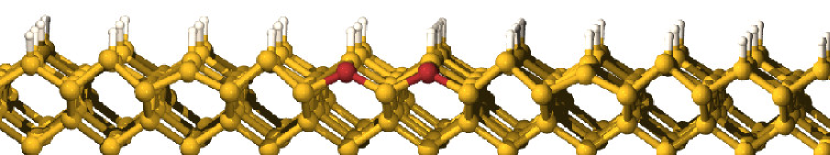
The solitons are broadly localised as expected, which is shown in Figure 3. This is similar to the polaron seen in the same systemBowler and Fisher (2001); Todorovic et al. (2002) and indicates that the soliton is similarly weakly coupled to the bulk. The overall behaviour and form of the soliton in the DB wire is very different to the conjugated polymer system. In particular, the soliton is associated with a pair of atoms and has two forms, while in conjugated polymers it is associated with the bond lengths near a single atom, and has only one form.

IV Discussion and Conclusions
Although the dangling-bond system is too reactive to be a component of nanoscale circuitry, it does serve both as a potential model for the study of one-dimensional conductors and as a stepping stone to realisable useful systems, for example as a template for the deposition of metal atoms in linear features. As such it is important that systems can be modelled accurately and quickly. In this paper, we have demonstrated that tight-binding simulations are suitable for even-length wires and used such techniques to explore the stability of ordering defects in the Jahn-Teller alternating displacement seen in perfect dangling bond wires. We note that modelling of odd-length wires is complicated by the development of “level” atoms in the relaxed system. This appears to be related to difficulties in adequately modelling unpaired electrons using the tight-binding formalism; we have modelled these systems using spin-polarised DFT, reported elsewhereBird and Bowler (2003).
In the even length system, we demonstrate that “soliton” type defects, where alternation between up and down displacements is interrupted, are only eV less stable than the perfect wire, but are associated with strong effects on the edges on the valence and conduction bands, as shown in Figure 2, as a consequence of changes in hybridisation state. The presence of an “UU” defect leads to the formation of an isolated state 0.22 eV above the original valence band. A “DD” defect is associated with a state 0.1 eV below the original conduction band, although the conduction band energies should be treated with caution due to the nature of the parametrisation. We also demonstrate that these states contain large contributions from the atoms associated with the defect i.e localisation.
Acknowledgements.
We thank the UK Engineering and Physical Sciences Research Council for funding (CFB) and the Royal Society for a University Research Fellowship (DRB).References
- Lyding et al. (1994) J. Lyding, T.-C. Shen, J. Hubacek, J. Tucker, and G. Abeln, Appl. Phys. Lett. 64, 2010 (1994).
- Haldane (1981) F. Haldane, J. Phys. C 14, 2585 (1981).
- Peierls (2001) R. E. Peierls, Quantum Theory of Solids. (Oxford University Press, 2001), p. 108 ff., Oxford Classics Series, reprint of 1936 original.
- Jahn and Teller (1937) H. A. Jahn and E. Teller, Proc. Roy. Soc. A 161, 220 (1937).
- Heeger et al. (1988) A. J. Heeger, S. Kivelson, J. R. Schrieffer, and W. P. Su, Rev. Mod. Phys. 60, 781 (1988).
- König and Stollhoff (1990) G. König and G. Stollhoff, Phys. Rev. Lett. 65, 1239 (1990).
- Landau (1933) L. Landau, Phys. Z. Sowjetunion 3, 664 (1933).
- Ness and Fisher (1999) H. Ness and A. Fisher, Phys. Rev. Lett. 83, 452 (1999).
- Ness and Fisher (2002) H. Ness and A. Fisher, Europhys. Lett. 57 (2002).
- Hitosugi et al. (1999) T. Hitosugi, S. Heike, T. Onogi, T. Hashizume, S. Watanabe, Z. Q. Li, K. Ohno, Y. Kawazoe, T. Hasegawa, and K. Kitazawa, Phys. Rev. Lett. 82, 4034 (1999).
- Bowler and Fisher (2001) D. R. Bowler and A. J. Fisher, Phys. Rev. B 63, 035310 (2001).
- Todorovic et al. (2002) M. Todorovic, A. Fisher, and D. Bowler, J. Phys.: Condens. Matter 14, L749 (2002).
- Goringe et al. (1997) C. M. Goringe, D. R. Bowler, and E. Hernandez, Rep. Prog. Phys. 60, 1447 (1997).
- Healy et al. (2001) S. B. Healy, C. Filippi, P. Kratzer, E. Penev, and M. Scheffler, Phys. Rev. Lett. 87, 16105 (2001).
- Bird (2001) C. F. Bird, MSci Project Report, CMMP, Physics Dept., University College London (2001), URL http://www.cmmp.ucl.ac.uk/~cfb/DB_wire_Si.pdf.
- Bowler et al. (1998) D. R. Bowler, M. Fearn, C. M. Goringe, A. P. Horsfeld, and D. G. Pettifor, J. Phys.: Condens. Matter 10, 3719 (1998).
- Monkhorst and Pack (1976) H. J. Monkhorst and J. D. Pack, Phys. Rev. B 13, 5188 (1976).
- Bird and Bowler (2003) C. F. Bird and D. R. Bowler, Surf. Sci. submitted (2003), cond-mat/0301592.
- Sutton et al. (1988) A. P. Sutton, M. W. Finnis, D. G. Pettifor, and Y. Ohta, J. Phys. C: Solid State Physics 21, 35 (1988).