Spin relaxation in (110) and (001) InAs/GaSb superlattices
Abstract
We report an enhancement of the electron spin relaxation time () in a (110) InAs/GaSb superlattice by more than an order of magnitude (25 times) relative to the corresponding (001) structure. The spin dynamics were measured using polarization sensitive pump probe techniques and a mid-infrared, subpicosecond PPLN OPO. Longer times in (110) superlattices are attributed to the suppression of the native interface asymmetry and bulk inversion asymmetry contributions to the precessional D’yakonov Perel spin relaxation process. Calculations using a nonperturbative 14-band nanostructure model give good agreement with experiment and indicate that possible structural inversion asymmetry contributions to associated with compositional mixing at the superlattice interfaces may limit the observed spin lifetime in (110) superlattices. Our findings have implications for potential spintronics applications using InAs/GaSb heterostructures.
Semiconductor heterostructures based on the InAs/GaSb/AlSb system have gained attention recently for potential applications in the rapidly growing field of semiconductor-based spintronics,Cartoixa:2001 ; Hammar:2002 ; Gilbert:2002 ; Heida:1998 in which the focus is to develop novel electronic devices and circuits that exploit the spin property of the electron.Wolf:2001 ; ALS:book By utilizing some of the unique characteristics of the InAs/GaSb/AlSb system, including the strong spin orbit interaction in InAs and GaSb, the ability to form a variety of interface types (type-I, type-II staggered, and type-II broken gap), and the high electron mobility of InAs, it may be possible to realize a host of novel high-speed spin-sensitive electronic devices. A crucial factor in the design of any spin-sensitive electronic device is the electron spin relaxation time (T1), which must be sufficiently long to allow for transport andor processing of the spin-polarized electrons. In InAs/GaSb/AlSb heterostructures, which contain bonds between semiconductor constituents with no atom in common, the nature of the interfaces can have a dramatic influence on the electron spin dynamics. The electron spin relaxation time was recently measured in (001) InAs/GaSb superlattices,Olesberg:2001 where it was found that the asymmetric potential at the interfaces, referred to as native interface asymmetry (NIA),ALS:book ; Olesberg:2001 ; Lau:2002 ; Vervoort:1999 ; Krebs:1996 strongly dominates the precessional spin relaxation process. In addition to affecting the band gap and intervalence band absorption properties of these superlattices,Lau:2002 NIA leads to spin relaxation times 1 ps, which are more than an order of magnitude shorter than expected considering bulk inversion asymmetry (BIA)Lau:2001 contributions alone.
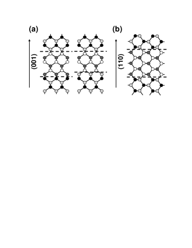
The interface contribution to spin relaxation in these no-common-atom superlattices may be removed through (110) growth, since the mixed anion-cation interface planes in this orientation lead to a symmetric interface potential. (See Fig. 1.) Since NIA strongly dominates spin relaxation in (001)-oriented InAs/GaSb superlattices, the electron spin lifetime is expected to be considerably longer in (110) InAs/GaSb superlattices. Additionally, suppression of the BIA contribution in (110) heterostructures has been predictedDK:1986 and recently verified experimentally in GaAs/AlGaAs quantum wells.Ohno:1999 This suppression has not been seen in any other material system. Here we observe it in InAs/GaSb superlattices.
We measured spin relaxation times in (110) and (001) InAs/GaSb superlattices using a mid-infrared femtosecond optical parametric oscillator and polarization sensitive differential transmission experiments. We observed an increase in by more than an order of magnitude for (110) growth. Theoretical calculations using a nonperturbative 14-band nanostructure model agree well with experiment. Due to the suppression of NIA and BIA contributions to spin relaxation in (110) InAs/GaSb superlattices, our calculations indicate that is highly sensitive to asymmetry arising from compositional mixing at the superlattice interfaces, an effect that may limit in (110) InAs/GaSb superlattices.
The InAs/GaSb superlattices were grown by molecular beam epitaxy on (001) or (110)-oriented InAs substrates (+/- 0.1 degree) in a Fisons VG-80 machine equipped with shuttered EPI group-III evaporators and shuttered EPI valved group V cracker cells. The superlattice structures contain 2.1 nm thick InAs layers and 3.7 nm thick GaSb layers, with a total of 85 periods. The (110) and (001) superlattices were grown in consecutive runs to minimize differences in extrinsic sample characteristics. X-ray diffraction measurements indicate high order resolution of the SL peaks, and features of the RHEED pattern are highly streaked, indicating good quality superlattice growth. The room temperature continuous wave photoluminescence signal from the superlattices was of similar intensity and line width for the (001) and (110) structures, and the carrier recombination time, measured by time-resolved photoluminescence up-conversion experiments, was found to be similar in the two superlattices (1-2 ns), indicating consistency of sample quality.
times were measured at low temperature (115 K) using pump probe experiments involving 200 fs, circularly polarized mid-infrared pulses (4.0-4.6 m). The laser source for these measurements is an optical parametric oscillator (OPO) that relies on parametric down conversion in a 1 mm thick periodically poled LiNbO3 (PPLN) crystal.Ebrahimzadeh:2001 The OPO is synchronously pumped by a Titanium sapphire oscillator, and provides 20 to 100 mW of average idler output power over the spectral tuning range (2.7-4.6 m). The output pulses have a full-width at half maximum bandwidth of 18 meV.
The confinement-induced splitting of the band edge heavy-hole and light-hole states is calculated to be 130 meV for the (001) and (110) InAs/GaSb superlattices considered here. In this case, circularly polarized idler pulses tuned close to the band gap will excite only the heavy-hole to conduction band transition, leading to a 100% spin-polarized distribution of electrons. The band gap of the (110) superlattice is slightly lower ( 40 meV) than the corresponding (001) structure. Band structure calculations for these superlattices suggest that this difference is due to lower electron and hole confinement energies in the (110) superlattice in addition to the differing influence of strain for different directions of superlattice growth. In order to compare measured spin lifetimes for identical electron kinetic energies, the OPO was tuned to 35 meV above the band gap for each structure. The limited tuning range of the OPO, together with the low band gaps of the InAs/GaSb superlattices studied [240 meV (110) and 280 meV (001) at 77 K], restricted our experiments to temperatures between 77 K and 115 K, over which the spin lifetimes were not found to vary significantly.
The optically-injected spin-polarized electrons generate absorption bleaching of the associated interband transition through state filling. By monitoring the transmission of a weaker, delayed probe pulse that has the same (SCP) or opposite (OCP) circular polarization as the pump pulse, may be extracted. The differential transmissivity was measured versus the time delay between the pump and probe pulses using a liquid N2-cooled InSb detector and lock-in detection methods. In our experiments, care was taken to ensure that the pump beam impinges on the superlattice sample at normal incidence. In this case, the probe beam interrogates the relaxation time of electron spins polarized in the growth direction. The optically injected carrier density was estimated using the measured pump pulse fluence and the calculated absorption spectrum for each structure to be 11016 cm-3 for (110) and 31016 cm-3 for (001), with an uncertainty of 40 %.
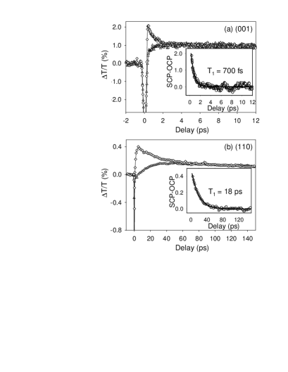
Fig. 2 shows the results of polarization-sensitive differential transmission measurements on InAs/GaSb superlattices with (001) (Fig. 2(a)) and (110) (Fig. 2(b)) directions of growth. Note the time scales on the x-axes in Fig. 2(a) and Fig. 2(b), which differ by more than an order of magnitude. The large negative pulse-width-limited feature appearing in both data sets originates from two-photon absorption in the InAs substrates. This feature provides a convenient marker for zero time delay, but may otherwise be ignored for the purpose of this discussion. The loss of spin polarization in the optically-injected carrier distribution is indicated by the convergence of the differential transmission signals for the SCP and OCP polarization geometries. ¿From a comparison of the data in Fig. 2(a) and Fig. 2(b), it is clear that spin relaxation occurs on a much longer time scale in the (110) InAs/GaSb superlattice compared to the (001) structure. The OCP signal in Fig. 2(b) grows from , indicating that the optically excited carriers are initially fully spin polarized, and that no detectable Coulomb screening effects are present. In the data for the (001) superlattice in Fig. 2(a), the non-zero bleaching signal in the OCP data immediately following the two-photon absorption feature is evidence of spin decay during pulse overlap. times are obtained by performing a single exponential fit to the difference between the SCP and OCP curves. Fits were restricted to delay values 350 fs to avoid the two-photon absorption feature. From the data in Fig. 2, we find values of 700 fs and 18 ps for the (001) and (110) superlattices respectively, indicating that the spin relaxation time in InAs/GaSb superlattices is strongly enhanced with (110) growth.
The much longer spin lifetime in the (110) InAs/GaSb superlattice relative to the corresponding (001) structure is primarily attributed to the elimination of the NIA contribution to spin relaxation. Although a larger is expected in (110) superlattices due to suppression of BIA,DK:1986 for the short period no-common-atom superlattices investigated here the more crucial distinction arises from the nature of the interfaces. Fig. 1 contains a schematic diagram of the interfaces in InAs/GaSb superlattices for conditions of growth along the (001) [Fig. 1(a)] and (110) [Fig. 1(b)] directions. For the (001) superlattice, the potential at the interfaces is asymmetric due to tetrahedral bonding between the bulk constituents (InAs and GaSb) that share no atom in common. This effect is referred to as NIA. As in the case of BIA, NIA generates a pseudomagnetic field that serves to relax the electron spins. It has been shown previouslyOlesberg:2001 that NIA strongly dominates the electron spin decay process in a similar (001)-oriented InAs/GaSb superlattice grown on a GaSb substrate. The subpicosecond spin lifetime extracted from the data of Fig. 2(a) is consistent with these earlier studies.Olesberg:2001 In contrast, for an InAs/GaSb superlattice grown in the (110) direction, NIA is absent because the interfaces are mixed, containing equal numbers of both anions and cations (see Fig. 1(b)). In this case, the interface potential is symmetric. Since spin decay in the (001) superlattice is strongly dominated by NIA, with its elimination in the (110) structure the spin lifetime is expected to sharply increase, consistent with the results in Fig. 2(b).
In order to interpret these findings, we have performed calculations of spin relaxation times due to the precessional D’yakonov Perel mechanism, which has been found to dominate in III-V semiconductors and their heterostructures for temperatures above 77 K.ALS:book ; Olesberg:2001 ; Lau:2001 ; OpticalOrientationBook ; Kikkawa:1998 ; Tacheuchi:1997 ; Terauchi:1999 ; Boggess:2000 We employ a nonperturbative nanostructure model solved in a fourteen-band restricted basis set, in which BIA contributions are included naturallyLau:2001 and NIA contributions are introduced as previously described.Olesberg:2001 Parameters governing the interface asymmetry were taken from reference 7. Neutral impurities were taken as the dominant source of momentum scattering. The spin lifetime varies inversely with momentum scattering time, . We find good agreement with experiment using = 190 fs, which is within the typical range (100-200 fs) for the III-V semiconductors.
The calculated spin relaxation time for the (001) superlattice is = 715 fs in good agreement with the experimental value of 700 fs. NIA was found to strongly dominate the electron spin relaxation process for the (001) structure, consistent with earlier findings.Olesberg:2001 For the (110) InAs/GaSb superlattice, our calculations indicate that, with the elimination of NIA and the strong suppression of the remaining BIA contribution,DK:1986 the spin lifetime is expected to be 600 ps. The much shorter observed experimentally (18 ps) indicates that additional contributions to the spin relaxation process are present and substantially dominate over BIA. The electron-hole exchange interaction (the Bir-Aronov-Pikus mechanismBAP:1976 (BAP)) is not a favorable candidate to account for the measured spin lifetime in the (110) superlattice due to the small electron-hole overlapWagner:1993 ; Vinattieri:1993 characteristic of these broken-gap InAs/GaSb superlattices (roughly 20% compared to GaAs/AlGaAs quantum wells) and because the timescale of spin decay (18 ps) is much shorter than that found previously for the BAP interaction.Ohno:1999 ; OpticalOrientationBook The Elliott-Yafet mechanism, which increases in importance with decreasing band gap,OpticalOrientationBook ; Chasalviel:1975 may limit in (110) InAs/GaSb superlattices, although a detailed theoretical treatment for this mechanism in III-V semiconductor superlattices is not presently available.
Because of the large spin-orbit interaction and small band gap in InAs/GaSb superlattices, a substantial contribution to the spin decay process could arise from a small degree of structural inversion asymmetry (SIA) associated with compositional mixing at the superlattice interfaces. In order to assess the sensitivity of to such effects, the spin lifetime was calculated assuming that the interface on one side of the InAs layers is not compositionally abrupt, corresponding to a single monolayer of In0.5Ga0.5As0.5Sb0.5. Such a situation may arise due to differing growth kinetics at the normal and inverted interfaces, an effect which is commonly present in InAs/GaSb superlattices.Feenstra:1994 ; Steinshnider:2000 ; Lew:1997 ; Wang:1995 With the inclusion of the mixed composition monolayer, the calculated spin lifetime in the (110) InAs/GaSb superlattice was reduced by a factor of 20, yielding a value of 29 ps, in line with the experimental value of 18 ps. This dramatic reduction in occurs because, although the pseudomagnetic field associated with BIA is primarily in the growth direction for (110)-oriented superlattices, SIA introduces a field component in the plane of the superlattice that serves to relax the growth-direction polarized electron spins injected in these optical experiments. In contrast, for the (001)-oriented superlattice including such compositional mixing has a much smaller influence on the calculated spin lifetimes because, for (001) superlattices, both the psuedomagnetic fields associated with BIADK:1986 and NIA have large in-plane components. Detailed STM characterization of the present (110) superlattice would help in the conclusive identification of the physical process limiting .
In summary, we observe an enhancement of the electron spin relaxation time in InAs/GaSb superlattices by more than an order of magnitude (25 times) with (110)-oriented growth using polarization sensitive pump probe techniques and a mid-infrared, subpicosecond PPLN OPO. This enhancement is attributed to suppression of the NIA and BIA contributions to the spin decay process in (110) superlattices. Our findings have implications for potential spintronics applications using InAs/GaSb heterostructures.
This research is supported by the DARPA MDA972-01-C-0002, DARPA/ARO DAAD19-01-1-0490 and the Natural Sciences and Engineering Research Council of Canada.
References
- (1) X. Cartoixa, D. Z. Y. Ting, E. S. Daniel, and T. C. McGill, Superlattices and Microstructures 30, 309 (2001).
- (2) P. R. Hammar and Mark Johnson, Phys. Rev. Lett. 88, 066806 (2002).
- (3) M. J. Gilbert, J. P. Bird, T. Sugaya, R. Akis, Physica B 314, 230 (2002).
- (4) J. P. Heida, B. J. van Wees, J. J. Kuipers, T. M. Klapwijk, and G. Borghs, Phys. Rev. B 57, 11 911 (1998).
- (5) S. A. Wolf et al., Science 294, 1488 (2001).
- (6) Semiconductor Spintronics and Quantum Computation, edited by D. D. Awschalom, D. Loss, and N. Samarth (Springer-Verlag, Berlin Heidelberg New York, 2002).
- (7) J. T. Olesberg, W. H. Lau, M. E. Flatté, C. Yu, E. Altunkaya, E. M. Shaw, T. C. Hasenberg, and T. F. Boggess, Phys. Rev. B 64, 201301 (2001).
- (8) W. H. Lau and M. E. Flatté, Appl. Phys. Lett. 80, 1683 (2002).
- (9) L. Vervoort, R. Ferreira, and P. Voisin, Semicond. Sci. Technol. 14, 227 (1999).
- (10) O. Krebs and P. Voisin, Phys. Rev. Lett. 77,1829 (1996).
- (11) W. H. Lau, J. T. Olesberg, and M. E. Flatté, Phys. Rev. B 64, 161301 (2001).
- (12) M. I. D’yakonov and V. Yu. Kachorovskii, Sov. Phys. Semicond. 20, 110 (1986).
- (13) Y. Ohno, R. Terauchi, T. Adachi, F. Matsukura, and H. Ohno, Phys. Rev. Lett. 83, 4196 (1999).
- (14) M. Ebrahimzadeh, P. J. Phillips, and S. Das, Appl. Phys. B 72, 793 (2001).
- (15) Optical Orientation, edited by F. Meier and B. P. Zakharchenya (North Holland, New York, 1984).
- (16) J. M. Kikkawa and D. D. Awschalom, Phys. Rev. Lett. 80, 4313 (1998).
- (17) A. Tackeuchi, O. Wada, Y. Nishikawa, Appl. Phys. Lett. 70, 1131 (1997).
- (18) R. Terauchi, Y. Ohno, T. Adachi, A. Sato, F. Matsukura, A. Tackeuchi, H. Ohno, Jpn. J. Appl. Phys. 38, 2549 (1999).
- (19) T. F. Boggess, J. T. Olesberg, C. Yu, M. E. Flatté, and W. H. Lau, Appl. Phys. Lett. 77, 1333 (2000).
- (20) G. Bir, A. Aronov, and G. Pikus, Zh. Eksp. Teor. Fiz. 69, 1382 (1975) [Sov. Phys. JETP 42, 705 (1976)].
- (21) J. Wagner, H. Schneider, D. Richards, A. Fischer and K. Ploog, Phys. Rev. B 47, 4786 (1993).
- (22) A. Vinattieri, J. Shah, T. C. Damen, K. W. Goossen, L. N. Pfeiffer, M. Z. Maialle, and L. J. Sham, Appl. Phys. Lett. 63, 3164 (1993).
- (23) J.-N. Chazalviel, Phys. Rev. B 11, 1555 (1975).
- (24) R. M. Feenstra, D. A. Collins, D. Z.-Y. Ting, M. W. Wang, and T. C. McGill, Phys. Rev. Lett. 72, 2749 (1994).
- (25) J. Steinshnider, J. Harper, M. Weimer, C.-H. Lin, S. S. Pei, and D. H. Chow, Phys. Rev. Lett. 85, 4562 (2000).
- (26) A. Y. Lew, S. L. Zuo, E. T. Yu, R. H. Miles, Appl. Phys. Lett. 70, 75 (1997).
- (27) M. W. Wang, D. A. Collins, T. C. McGill, R. W. Grant, R. M. Feenstra, J. Vac. Sci. Technol. B 13, 1689 (1995).